Radar target detection system for autonomous vehicles with ultra-low phase noise frequency synthesizer

An object detection system for autonomous vehicle, comprising a radar unit and at least one ultra-low phase noise frequency synthesizer, is provided. The radar unit configured for detecting the presence and characteristics of one or more objects in various directions. The radar unit may include a transmitter for transmitting at least one radio signal; and a receiver for receiving the at least one radio signal returned from the one or more objects. The ultra-low phase noise frequency synthesizer may utilize Clocking device, Sampling Reference PLL, at least one fixed frequency divider, DDS and main PLL to reduce phase noise from the returned radio signal. This proposed system overcomes deficiencies of current generation state of the art Radar Systems by providing much lower level of phase noise which would result in improved performance of the radar system in terms of target detection, characterization etc. Further, a method for autonomous vehicle is also disclosed.

Recommended
Recommended
More Related Content
Similar to Radar target detection system for autonomous vehicles with ultra-low phase noise frequency synthesizer
Similar to Radar target detection system for autonomous vehicles with ultra-low phase noise frequency synthesizer (20)
More from Tal Lavian Ph.D.
More from Tal Lavian Ph.D. (20)
Recently uploaded
Recently uploaded (20)
Radar target detection system for autonomous vehicles with ultra-low phase noise frequency synthesizer
- 1. MAIMUUNMUNTANTULMUTLU ONA TIUS009831881B2 (12)United States Patent Josefsberg et al. (10) Patent No.: US 9,831,881 B2 (45) Date ofPatent: Nov.28,2017 (54) RADAR TARGET DETECTION SYSTEM FOR AUTONOMOUS VEHICLES WITH ULTRA -LOW PHASE NOISE FREQUENCY SYNTHESIZER (58) Field of Classification Search CPC . HO3L 7 /085; HO3L 7 /02; HO3L 7 /099; HO3L 7 /113; HO3L 7 /185 ; HO3L 7 /20; HO3L 7 /23; HO3L 7 /24; HO3L 7 /00; HO3L 7/06; GO1S 7/031; G01S 12/931; G01S 13/931 USPC ...... . 342/128, 70, 99- 104; 327/145, 105, 327/147–159; 701/301; 455/90.1 See application file for complete search history. (71) Applicants:Yekutiel Josefsberg,Netanya (IL ); Tal Lavian, Sunnyvale, CA (US) (72) Inventors: Yekutiel Josefsberg, Netanya (IL ); Tal Lavian, Sunnyvale, CA (US) Subject to any disclaimer,the term ofthis patent is extended or adjusted under 35 U .S.C. 154(b) by 0 days. (56 ) References Cited U.S. PATENT DOCUMENTS 6,085,151 A * 7/2000 Farmer ............. (21) Appl.No.: 15/640,904 7,737,880 B2 * GO1S 7/023 342/70 GOIS 7/023 342/100 6/2010 Vacanti (22) Filed: Jul. 3,2017 (Continued) (65) Primary Examiner — Dinh T LePrior Publication Data US 2017/0302282 A1 Oct. 19, 2017 Related U .S. Application Data (63) Continuation-in-part of application No. 15/379,860, filed on Dec. 15, 2016, now Pat. No. 9,729,158, (Continued) (51) Int. CI. GOIS 13/524 (2006.01) HO3L 7/085 (2006.01) HO3L 77099 (2006 .01) HOZL 7/07 (2006.01) HO3L 7/23 (2006.01) (Continued) (52) U.S.CI. CPC ............. HO3L 7/085 (2013.01); GOIS 7/023 (2013.01); HO3L 7/07 (2013.01); HO3L 77099 (2013.01); HO3L 7/113 (2013.01); HO3L 7/185 (2013.01);HO3L 7/20 (2013.01); HO3L 7/23 (2013.01);HO3L 7/24 (2013.01);GOIS 13/931 (2013.01) (57) ABSTRACT An object detection system for autonomous vehicle, com prising a radar unit and at least oneultra-low phase noise frequency synthesizer, is provided. The radar unitconfigured fordetecting the presence and characteristics ofone ormore objects in various directions. The radar unit may include a transmitter for transmitting at least one radio signal, and a receiver forreceiving the at least one radio signalreturned from the one or more objects. The ultra -low phase noise frequency synthesizer may utilize Clocking device, Sam pling Reference PLL, at least one fixed frequency divider, DDS and main PLL to reduce phase noise from the returned radio signal. This proposed system overcomes deficiencies of current generation state of the art Radar Systems by providing much lower level of phase noise which would result in improved performanceofthe radar system in terms of target detection , characterization etc. Further, a method for autonomous vehicle is also disclosed. 20 Claims, 40 Drawing Sheets DetectingSystem 3702 3706 RadarUnit Memory 3710 3704 Instructions set 3712 Low Phase Noise frequency synthesizer Database Processor 3700
- 2. US 9,831,881B2Page 2 Related U .S. Application Data which is a continuation of application No. 15/229, 915, filed on Aug.5, 2016 ,now Pat.No. 9,705,511. (60) Provisional application No.62/181,221, filed on Jun. 18, 2015. (51) Int. Cl. HOZL 7/20 HO3L 7/185 HO3L 7/113 HO3L 7/24 GOIS 7/02 GOIS 13/93 (2006 .01) (2006 .01) (2006 .01) (2006 .01) (2006.01) (2006 .01) (56 ) References Cited U.S.PATENTDOCUMENTS 8 ,049,656 B2* 11/2011 Shani G01S 77021 342/13 9 ,470,784 B2 * 10/2016 Kishigami .............. GO1S 13/91 9,689,983 B2 * 6/2017 Cao ....................... G018 13/931 * cited by examiner
- 3. U. S . Patent Nov.28,2017 Sheet 1 of40 US 9,831,881 B2 -10 ?? MAMAHA ??????????? ??AXO NAL_MACHANE 06 ???????????????????? ?? FIG.1 2 ? ARACLE:ZHEJAPAPANYREAL ???
- 4. 200 ** *** U .S . Patent 202 204 206 208 TOWWWWWY*XXXYYIK IWAYAXWXY Mtiivi Fout Loop MerrnHTROOK Fclock Reference Phase Clock detector www VA VCOWYKYKYMYAYISYYTY W TRAB HXHEY filter Nov.28,2017 VP???????????????????? WAMI PETENSI Fclock- WARY Divider Sheet 2 of40 +* A49265917 W W9144447714727WW949*407472999697989649W 210 N WOWYWIwMTY244AYAAVANI SWcontrol FIG.2 US 9,831,881 B2
- 5. U .S . Patent 300 ****** 304 Nov.28,2017 YNAYYNAMYYYYYYYYY Fclock PED AVVAvYW4V VREMSANNSYANVAR VANNY TYTYYYYYSTAWY FoutN TYWYYTYYTYVYYTYYTY YMYWYYNY *wm Sheet 3 of 40 VALOXBLLOK U SUWOWEN FIG.3 US 9,831,881 B2
- 6. U .S. Patent Nov. 28, 2017 Sheet 4 of 40 US 9,831,881 B2 FREE THAAAAAAAAWITHHANA PROPHOT CeLALALA |402129F AHA FIG.4 / C3 989REATA ALLEAL TANIAAAAAAAAAA NONEW
- 7. U .S . Patent Nov.28,2017 Sheet 5 of40 US 9,831,881 B2 OUTPUTfilmikriitiderke wwwww * * ** * ** w.w *** w * * * * * * * *** *Wi SAMPLECONTROLC distrimit watuOmano FIG.5 OUTPUTINPUT wwwmums itininiai w* CH har *** * * ** *** ** * *** *** * ** *** ** *** * ** ** * * * * ** * *** *** * wwwminiwmiwa SAMPLECONTROLwwwwwwwwwwx INPUT
- 8. U .S . Patent PRATTUT TON TO T win ZUTA VAMZAWAYLYLLAHA 604. 602RF ERRORVOLTAGE Nov.28,2017 20 WWW:MRM 00MHZ INPUT SRD ** INPUTYA ALLAH 7 YYRYYYYYYYYYYY WE 606 } Sheet6 of 40 UWAUAWASAVYOWAWEANSross YO + WA FIG.6 US 9,831,881 B2
- 9. U .S . Patent Nov.28,2017 Sheet 7 of40 US 9,831,881 B2 ? - -- Sunwind IN d ------- im - Flapper nasprotiobuna ata cancelamentoensinomasselfoongtaon sercise nestiw *+-*+- w . d A VV . wwwwww FIG.7 par ? d restierikw tym w hanguiniffinitions thisinformasi ** weitefrana *** broodfrom finansnetton past wantfor theroom wesentlo ngbansasenseofse vese scenes bebas
- 10. U .S . Patent Nov.28,2017 Sheet 8 of40 US 9,831,881 B2 eurde Phasenoise 208 *** WAXWXR O VLADARAKAVA PARANAVARRARANDARARAMDARBAROS PAUKSONAYSEXY FIG.8 r **** 800
- 11. U .S . Patent Nov.28,2017 Sheet 9 of40 US 9,831,881 B2 OSIONOSOud 006. A 904 prisiprie pupuna FIG.9 sesinaisestiXXXXXX 00ADuringandSONSed ************** ********* Hier4 *** 902istiyotlight *** *************** PhaseNoise
- 12. US 9,831,881 B2 ?000 ? ??????????? ? ? ? ? ? ? ? ???? ? ? ??????? ? ? ??? ? ? ? ??????????????????? ???????????????? ????????? ?????????? ??????? ?????? ???? ? 1006? ????????????. ??? ? ?? ? ??????????????????????? ? ? ?? ? ? ? ? ? ? ?? ???????? ? ? ??? ? ??? ? ? ? ? ? ??? ?.. ??.? ?????? ????? Sheet 10Of 40 ? , ????????????????????????? ? ? ? ? ?? XXX-XXx ?? ? ? ????? - ? FIG, 10 ? ? ??? ? . ? ? ? ??????.? ????????? ?? ?? ??? ? ? ???????????????? ???????????????? ? ? ? ? ? ? ??? ????????? ? ?.??? ? ?? :*????????8%?????????????? ? ???????????????????????????????? ??? ? ? ? ????? ??????? ??? ?? ? ? ? ? ? ?? ???????? ! ' ???? {{004 ?? ??? ??? ? ?? ?????? _ ,;tterriir? ????????? ? ? ? ? ? ? ? ???????????:???:??:mmif ? ? ?- ? ? ? ????????????????????????????????? ?????? ??????? ;.???????? ? ?????????? ?????? ??????????? ?????? ????? ??? ? ?? ? ????????. 1002 Nov.28, 2017 ? ? ??????????! wv-****** * *** * ** ** **** ** ? 3 3?_ _ . ? ? ?????}??83.. ?????????????????????????????????????????:?????????:?.:::::???:?????.; ? ' ??????????XX?}}'????????????????? U,S, Patent
- 13. atent Nov. 28, 2017 Sheet 11 of 40 US 9,831,881 B2 MOBO soydBanks osvendoocon Q Www ** ** INN('ncaoz FIG.11** ***** 1102 1104 aniood******** :. 1100 wwwwwwwwwwwww
- 14. U .S. Patent Nov.28,2017 Sheet 12 of 40 US 9,831,881 B2 MOZW send Singlesidebandphasenoise FIG.12 1200
- 15. U .S. Patent Nov.28,2017 Sheet 13 of 40 US 9,831,881 B2 312* 13041304 1302 W210) 1316 1310 GY62 FIG.13 edor 1308 ***** * **** 13181306 ** * 1300
- 16. U .S . Patent 1400 1402 Nov.28,2017 1404 14061406 1408 1410 robecareestepersonwithlongcomoCamping TCXO movieLoopiter the Vco erater toget wwwwwwwwwwwwwww Sheet 14 of 40 FIG.14 US 9,831,881 B2
- 17. U .S. Patent Nov.28,2017 Sheet 15 of 40 US 9,831,881 B2 1504 DOGLUWWW min 1508 VBULSEWÁN GENERATOR 1502 we who FIG.15 1506 1500
- 19. U .S . Patent 1700 1702 1704 1706 1708 ons 170417081798thenex-Manipulad1716 X8mm wiiiiiii O Nov.28,2017 1710 1716716 3 wwwwwwwwwwwwwwwwwwwwwwwwwwwww 1714 1712 anno1720 SwingVoce Sheet 17 of 40 en1718 ««««««««« SamplingPull 1724 1722 FIG.17 US 9,831,881 B2
- 20. U .S . Patent 1800 1804 *** * * * * * * * * 1802 1810 1814 1806 Synthesizer **...* * Nov.28,2017 W CXO wwwwww X8 W* Detecto * * 1812 wwwW ****** wwwwwww * 1816 ** ** ** * * * ** ** **** Sheet 18 of 40 wwwwwwwwwwwwwwwww SampoVale 1818 1820S 1822 ingul WWWWWWWWWWWWWWFIG.18 US 9,831,881 B2
- 21. U .S . Patent 1900 1916 Nov.28,2017 1902 III-ILLILILI-II-II-ILLILI-LII. fas 1904 SamplingPL comb Comb GamingVSDCswitchLoopL M135 generator Olter détector CXOLO www VCO 19081910 1906 1912 Sheet 19 of 40 DigitalPLL 0000000000000000000000000000000000000OCCA DigialphraseFrequencyDetector 1918 1914 FIG.19 US 9,831,881 B2
- 22. U .S. Patent Nov.28,2017 Sheet 20 of 40 US 9,831,881 B2 2006 2008 OLOZ*2012 Ver Rioolwou W.2004 www W wwwwwwwwwwwwwwwwwwwwwwwwwwww 2001FREQUENCYOFFSET(MX} FIG.20 BOL1 00 wwwww wwwwwwwwwwwwwwww OL 2000 PHASENOISE(dBc/M2) 2002
- 23. US 9,831,881 B2 Col4? 504/ ??????????????XM??'0?}_ ?? ??? ? _ fi f }}ff ??? ff; .????????? ???? ?" "? ?"?? ? ?????? ????? ????.???? ????:?????? ? ? ? ??? . ?? ?? ,:;;:? ???? ?????..? ? ???.??:; ??????? ???? ????;.:??.? ??????????::.;.;;;:? ???????????????? ??????? ??????;;_ ?????? y++C ?? ??? ????????:;";? ? ? ????? m ? ?.? Sheet 21 Of 40 ? ??. ? ????.? ???? ? 3%8k ??.?.:??:??? ?????????? ???????? ?????? ? ??????? *?? ???????+8%??????????????????? CLLC ?? ???????????????????????????????, ????? ????????? ???:;??? ?????????????:4??????????? ???..?????.??..?.?????? ?????????????? ????????? ????:__.;????:???::;?3? ???????????????;???????? ?????????.????:; * ***.??????????? ;:?????? ????????.???? ??ct A ?????????? .???? ??????? ?** C00/ XIX; 3 ? ? ? ??????????????? ??????:; ??????? ?? ????????? ????????? ?? ? ??? ? ? ? ?? ?? ? -...… ?? ? ? ? 0LLC??]80?90 ???????;: ?????:::? ?? ?? ? ? ? ? ? ? ??????? ?????????????? ??????? ??????????????4 ?? ? ? ? ? ???? ??? ? ?????? ??? ????? ???????? ???:;? ???????..?? ...?... XXX 3 $ ? ? c ? ? ? ? ? ? ? ? X ?????????? ????.????????????? .???? ?????????????????:;:,? ?????????.???????????.? ?? ?.?????? ? ? ??????;3?? ????????? ???????? ?.?????????.??? ?_:'???? ????????? ????????? ??????? ???????? ????????? ?????????? ????????????? ???????? ???'?? ??????????????? ??? ? 3???? ????????? ???????????????? ??????? ?? ????? '..????? ?????? ??% ??????? ???? ?????????. ?.????f" ? ? . Nov.28, 2017 ?????????????? ::::3: ?????? ????&?.? ??? ?.?????? ??????? ??????? ? ? ? ?? ? ???? ???? ?;?? ??? ??? ? ?????? 3 ? ??????????????????? ? ?? ?????????????????????????????????? ????????????????????.??? ??.????? ????????3 :.????????????????|;.?????;: ???????:_ ??????????????}???????????????????;: ???????????????????????????:,?????????????.???????????? ?????????????????????????????????????????????????????????????????????????????????????????????????????????????????????????????????????????????????????????????????????????? ??.??? --- _ ? "?' ? 333333333831 001/ U, S, Patent
- 24. US 9,831,881 B2 2003?88?????????24 ????8} ???FH ? ? ?? }} }? ? ?? ? ????y???? ? ? 0>?0 ?»:«:? ??? ????? ? ??????????-]iwtwyrywr»«?????????????www???????????? ????????????????????????????????????????????? ????:::?? ??????????????? ???????.??????????????????? ?..????:;..????????????????? ????????;???????????????;:";? ?????????????????????????????-??????????????????? ???????????????????? ?????????? ..?????????????????????-?????????? ????}}} ???????? ???????????????????????????????.?.????? ??????????? ??????????? :???????? ??????? ?????????? ?????? ? ? ???????????????? ???????????????? ? ???????? ??:;;;:?????????4 ?????;????? ????????????? ??????? ?????LC+0 Sheet 22 of 40 ? ?????? ??? ? Z0ZZ 802/ Khán gi? 48048 ?????????? ?????? ??????? ???????? ????????? ???????????????? **; .?.?? 90Z2 ??.?..???.?.?? ?? ? ?? ?????????????????????????? ? ? ??? ???????????????????? ????? ????? ????}??????????? ? ????????????????????????????? ???????????????????????? ?????????????????????????:??????"??>?.??????????...|.. ?????????????????????????? ????????? ???????????????????????????? ???????????????????????????????????';????????????????.????|??????????????????? ???????..???????????????????????? ?'?? ??????--- ? ;..?..-- ? Nov.28, 2017 - ?.??? ? ?? ?? .? ???????. ??????? ? ?????? ? ? ? ?? ??? [???% 83%? Ftcgi/ XXXV????? 00Z U,S, Patent
- 25. US 9,831,881 B2 £/'lH 50£Z ????.?? ??? ? ? ? ? ??? ? ? ??????? ?XXX? ? ? ? ?? ?????? ? ? ? ? ? ? ??? ? ? ?? zte/ ? ??????? ? ?????????????????????? ???????????????????????????????????????????????;???????????? ????????????????????????????????????????? ????? ? ???? ? ?????? ? ? ?? ??? ?? ????????? ? Sheet 23 0f 40 ? ? ?? ??? ????? ? ???? ? ???????????? ? ? ? ????????????????? ??? ? ??0££Z ??????? ? ?..? ?? .C08/ ? ?????????????????????????????? ???????????????????? ?? ??? ???????????????????????????? ????????????? ???? ?????? $f1 ?????? ?? .? ? ??. ? ? ??? ??? ? ???? ?????????? ? ?????????????? ?????????????? ???????? ??????????????????.?????????? ?????????? ? ? ??????????????? ????????????????..?????????? ??????????????? ? ? ?? ? ???????????.????????????????? ????????.:'?????????? ????; ??????? ? ? ? ? ??? ????: ? ??? ?.??? ? ? ?? ' Nov.28, 2017 ..,. ??;:;:? ????????;.?????? ????????????????????????.???????????????????????????????????????????????????????????????.????????? ??????? ???;:;?? ?????? ???????????????????????????????????????????????? ???????????????????????????????????? ???? ???.?:?? ??????? ?????? ????::?? ?????:?????????????????????????????????????????; ???????????????? ????? ????????????????????? ? ? ? ? ,.? ? ??.?.? ?? ? ?? ?? ?? ? ??? 006/ U, S, Patent
- 26. US 9,831,881 B2 Cols PO'z ,??'fxffXVA / $ ry +++? : 1 ??? ? ? ?? ?? ?? -28 ? ?? ??? ? ? ? ??? ? ? ? ? ? ? ? ? .... .. . . . ..... ........ . .. ... .. ... i. .1 N4324 ? ??;:?? ? ? ??? ?_ ? ????? ????? ?????;!??? ?? ?? ? ???????????????? ????????? ?????? 37086 ????????? ? ? ? ? ????? ?? ? ?????::?? ?Z++0 4 ? Sheet 24 of 40 ???????? C0FC . ??????????? ? ;' fxssgoix?&fc£4z ? ? ? ? ? ? ..????????????????? .?????????????????????.?????????????????????????????????*??.???????????????? ????????????*?????? ?????????????? ?.???????? ????????????????????????. ??????????????????????????????????.??????????????? ?????:;?; *??????? ??????????????? ??????:;?????? ??????? ????????????????????????????????? ?? ?????????,????????????? ????????????????????????????????????????????? ????????????? ?????????????; ???????????? ???????????.? ??????? ? ??????????????????? .?.???? ?????????.?????????????;:?????i' ;;_;??????????????????????????:? ????????????????.???????????.???????? ?????????????????????..????????:? 83? ???????? ???????????????????????????????????? ?8 ?????????????????????????????? ?.????????? ???????????? ??????????????????????????????????????? ??????Z'90 ?' ? ? ? ??? ? ? ? ?? ?? Nov.28, 2017 ??? ? ??? ? ? ? ? ?.????????????????????????.??????????.? ? ?????????????????????????????? ????????????????? ?????? VACA' f 48F% 83% 88A? ?????????????????? 00Z U, S, Patent
- 27. US 9,831,881 B2 SCOld f0g/ ??8*2322%4f4 ? ? ?? ? ? ? ?? ? ? ? ???? ?????? ???????????????? ????????????????????????????? ????????????????????????????????????????????????? ? ??? ?? ???? ? ??????? ????????????? ???????? ?????????????? ??????????????????????????????????? ? ???? ? ? ??? ????????? ????????????;??????????????????????????? ????????????????? ??? ?? ??? ? ?? ? !0 Sheet 25 of 40 ????????? ?? ????????? ? ??????????? ?????????????????? ??????? ?? ??? ??? ???????????????? ?????} }}8 ??|.?|. ???????? ???????? ?? C09/ ?? ?? ????? ?? ?.?.'.? 90s/ ??????????????????????????? ????????????? ??????. ?????????????????????????? ?????????????? ?????????????????????????? ????????????? ?? ?????? ????? ?????????????????????????? ?????????????? ???????? ?? ?? ???????????????????????????? ??? ?? ??? ?????? ? ?????? ???? ? ?? ???? ? ? ? ????? ? ? ???? ????? ???????? ? ???? ?????????? ???????????????????? ???? ?..-..- 444 Nov.28, 2017 ???????? ??????????????????????? ???? ???????? ????. ?? ???????.?.;.??? ? ??????????????????????????????????????8 88?????????? ????????????????????????????????????????????????????? ???? ? 009/ U, S, Patent
- 28. US 9,831,881 B2 FIG.26 2604 k&ffi; & ????????????????????????? ? ? ???? ?? ;lf*€ ?} '!} **£ HH { JJ? ? ??? ????? ??? ? ??? ?? ? 4 ???? :;????????:* ?? ??? ????????????? ??????:;_ ???????? ??:?!:; ?????*. ;.;?????? ??? ????? ?????????:? ? ?? ? ?? ??????? ??????? ?? ?? ????? ? ???4 >219 ?????|??????? ????????? ????? ? ?????????????? ?????? ?? * . . * - * -"? ??:;"? ??????? ;;.; ????????° ????????? ??? ? ?? ?? ? ????????? ? ? ?????????????? ??:??? 2610? ??????? ????? ??????? ????????? ??????????? ?? ?? ?:?? ??????? ???????? ??? Sheet 26 of 40 ? 2602 ? ? ? ?? ? ? 809/: ??? ????:; ; -.. ???.-.--;.? ??? 82%2&?%82%8K8%82%XX 444444 '???????????????:? ?????? ???????????? ; :'?? ???? ? ?? ? ? ? ?????? * * * ? ? ! i; ? ????? ????????????????????????????????????????????????rnioqu ????..???? ? ? 2606??? ??? ? ? ? ??????? ? ? ???? ???? ? ?? ? ???? ?????????? ????. ?????:????????? ????????????????? ?????????????????? ? ???? ?? ?? ? ; ? ??? ? ?;.:! ? ?? ?? ?? ??????????????? ????? ?? ??? ?? ? ????? ?? . * . " . * * * ?? ???????? ????????? ?? ???????? ??????? ?? ? ??????? ?????? ???...-??-.- ???4????????. ??????? ???????? ??4???? ??????? ? ??????????. ?_.?????? ??????? ; ? ??..???????? ? ?? ? ???*?? ????:?' ? ? ?? ? ..? ?? ?? ??? ?? ?°? ?????? ?????? ?? ? ? ?????? ??? ? ???????? ?????? ????? ? ??:; ? ? ? ? ??k?? ???-? ?? ?????????3 ? ? Nov.28, 2017 ? ?????.?????? ???????? ???????? ? ?????????? ???? % AMM - A ? ???? ??? ???? ;.*.???????????????? ???????? % A4% 8 ? }$ --??????????? ???????? $$$$$$$; ?? ?? citt% ? ?????? ????? ?????:.. = 4 & ??? ?f ?? ?:4 ??????????????????????????????? ????? 4 }} 9C C4% suoinquuooOSIONIV ????? ?????? ??????????????????????????????????????? ????? 2600 U,S, Patent
- 29. U .S . Patent Nov.28,2017 Sheet 27 of 40 US 9,831,881 B2 DOLZ WWW o are SoSOSIALlontaKouko WooSoxmasesamo also900 9026 - . 7. . .7 . 7 . . . . . . wwwwwwwww 27913*************** 08-STKS Matag216 SongMoSanRIam KOONB umesShoesB QBORCERDD S YOUTUS MOBORE SOWIEDESS oogooe. DOO wwwwwwwwwwwwwwwwwwwwwwwwwwwwwwwwwwwwwwwwwwwwwwwwwww* * w www F *. * *. *. *. * *. * *. * *. * *. *. * *. * *. * *. *. *. * *. *. * *. * *. *. *. wwwwwwwwwwww SOMI SOLOOXOL100 DUODONQ MARIEOMX dues 80,Spo eX DOLZ
- 30. US 9,831,881 B2 87913 * W X WooLogoON WOWON on *44 9087. S WWWWWWWWW Sheet 28 of 40 www LOW OSOS B OXwwwwwwwwwwwwwwwwww 001SEOS 1087 2087 M ay Nov.28,2017 www MUSEOOmau U .S. Patent 0082
- 31. US 9,831,881 B2 FIG.29 EndtEnd cher -LULLILLLLL112-414144-141-LU. LUI-L114.114.1144471114_WJ.LIIJ.LUJJ1111111119 2906 "$Quouogelapasoodso Puesowadsuogompowyousoleselep YouOne0:192SousXoU90091SON3:20.Moeunuejocenas OURROUBOVadnow01116oulddiessyvumBeppesino2007 Sheet 29 of 40 ----- -2 -2 -2 2 ---- -- --2 --------2----2----- SRUusYoonDUSLUCOUuwasaidnou35oujeopjelugepuleseulisyogp OLSanaazooalad984dOujduasy 1062 wwwwwwwwwwwwwwwwww121*1 * 311424413623.41.41 :21:22 :14.233.242 :1-24 Nov.28,2017 2067 ZMNOSZOZHW000SOGUEROUNDSQUMOjosiaubisxpopsouboucoOXOLY 2900 U .S. Patent
- 32. U .S . Patent Nov.28,2017 Sheet 30 of 40 US 9,831,881 B2 * * . LIDAR"Deadzone" FIG.30A(PriorArt)
- 33. U .S . Patent Nov.28,2017 Sheet 31 of 40 US 9,831,881 B2 * * * * * * institutions wwwwww MODO** LIDARunitabovecar FIG.30B(PriorArt)www W * * VAR*! wwwwww w ét wa wwwww wwwwwwwwwww
- 34. US 9,831,881 B2 (wyjoud)LE'91 * ################################################# # ####################* suoppb?f?sparuemun Sheet 32 of 40 ***** **** * ** ** ??????-?SAHAPE od - - - -- --- Nov.28,2017 ***** * **** * * wy. U .S. Patent
- 35. U .S. Patent Nov.28,2017 Sheet 33 of 40 US 9,831,881 B2 entransmit ContinuousRadarContinuousRadar receive FIG.32 (PriorArt) arebooks10ftblindadvancementat65mph
- 36. U .S . Patent Nov.28,2017 Sheet 34 of 40 US 9,831,881 B2 :: RadarNotlimitedbylight camerelimitedLightedArea Notvisiblefor CamerasFIG.33 Radarbehindplasticparts
- 37. U .S. Patent Nov.28,2017 Sheet 35 of 40 US 9,831,881 B2 FastMovingObject ??????"Skirts SlowmovingObject A FIG.34(PriorArt)
- 38. Pulescompressed"returnsignal U .S. Patent ******** * ?? ?S Nov.28,2017 0.6 Sheet 36 of 40 wa FIG.35(PriorArt) US 9,831,881 B2
- 39. U .S . Patent Phasenoise"Skirt ElevatedSNRduetoPrase Noise Weaksignalsobscuredby????? Nov.28,2017 MoltipleReturnSignals Sheet 37 of 40 FIG.36 (PriorArt) US 9,831,881 B2
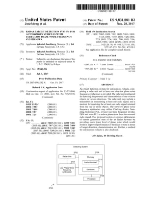
- 40. U .S . Patent DetectingSystem 3702 3706 Nov.28,2017 RadarUnit Memory 3710 3704 Instructionsset 3712 LowPhaseNoisefrequencysynthesizer Database Sheet 38 of 40 3708 Processor 3700 FIG.37 US 9,831,881 B2
- 41. U .S . Patent Nov.28,2017 Sheet 39 of 40 US 9,831,881 B2 -3804 3802 FIG.38 **** . bitrate 3800
- 42. U .S. Patent 3900 3902 detectingapresenceofoneormoreobjectsinoneormoredirectionsbyaradarunit Nov.28,2017 3904 Utilizingatleastoneultra-lowphasenoisefrequencysynthesizerforrefiningtransmittedandreceivedradarsignalsoftheradarunit 3906 Processingtherefinedreceivedradarsignalstodetermineoneormorecharacteristicsoftheobjects Sheet 40 of 40 3908 2 Enableautonomousvehicletoadoptoneormoreactionsbasedonthedeterminedcharacteristicsoftheobjects FIG.39 US 9,831,881 B2
- 43. US 9,831,881 B2 RADAR TARGET DETECTION SYSTEM FOR AUTONOMOUS VEHICLES WITH ULTRA-LOW PHASE NOISE FREQUENCY SYNTHESIZER inputs. For autonomous cars and other autonomousvehicles, the human sensesmustbe replaced with electronic sensors and the cognitive capabilities by electronic computing power. Themost common sensor technologies are as fol 5 lows: CROSS-REFERENCE TO RELATED LIDAR (Light Detection and Ranging)— APPLICATIONS is a technology thatmeasures distance by illuminating its surroundingswith laser light and receiving the reflections. This application is a continuation-in -part of U .S . appli- However, themaximum power of the laser lightneeds to be cation Ser. No. 15/379,860 filed on Dec. 15, 2016, is a 10 keptlimited to make them safe for eyes,as the laser lightcan continuation of U .S. application Ser.No. 15/229,915 filed on easily be absorbed by eyes. Such LIDAR systems are Aug. 5, 2016,now U .S. Pat. No. 9,705,511,which claims usually quite large,expensive and donotblend inwellwith priority to U .S. ProvisionalPatent Application No.62/181, the overall design of a car/vehicle. The weight of such 221 filed on Jun. 18, 2015,the disclosure ofwhich is hereby systemscan be as high as tens ofkilogramsand thecostcan incorporated by reference in its entirety. 13 be expensive and in some cases high up to $100,000. This patent application relates to the following co-as Radar (Radio Detection and Ranging) signed applicationsthatare each incorporated by reference: These days Radar systemscan be found as a single chip International Patent Application number PCT/IB2016 / solution thatis lightweight and cost effective. These systems 054790 filed on Aug. 9, 2016. U .S. Pat. No. 9,660,655 work verywellregardless oflighting orweather conditions granted May 23, 2017, based on U .S.application Ser. No. 20 and have satisfying accuracy in determining the speed of 15/379,915 filed on Dec. 15, 2016 . objects around the vehicle. Having said the above, mainly because of phase uncertainties the resolution of RadarFIELD systems is usually not sufficient. Ultrasonic Sensors Embodiments of the present disclosure are generally 25 These sensors use sound waves and measure their reflec related to sensors for autonomous vehicles (for example, tions from objects surrounding the vehicle. These sensorsSelf-Driving Cars) and in particularto systemsthatprovide are very accurate and work in every type of lighting condi ultra-low phasenoise frequency generation forRadar Appli tions.Ultrasonic sensors are also smalland cheap andwork cation for autonomous vehicles. well in almost any kind ofweather,but that is because of their very short range of a few meters.BACKGROUND Passive Visual Sensing This type of sensinguses cameras and image recognitionAutonomous Cars: algorithms. This sensor technology has one advantage that Levels of Autonomous Cars: none of the previous sensor technologies have colour andAccording to the Society ofAutomotiveEngineers (SAE) 35 contrastrecognition .Aswith any camera based systems,thecars and vehicles in general are classified into 5 different performance ofthese systemsdegradeswith bad lightingorclassifications: adverse weather conditions. Level 0: Automated system has no vehicle control, but The table below is designed to provide a better undermay issue warnings. standing ofthe advantages and disadvantages ofthedifferent Level1:Drivermustbe ready to take controlat any time. 40 currentsensortechnologiesand their overall contribution toAutomated system may include features such asAdap an autonomous vehicle:tive Cruise Control (ACC), Parking Assistance with The following tables scores the different sensors on aautomated steering, and Lane Keeping Assistance scale of 1 to 3, where 3 is the best score:(LKA) Type II in any combination. Level 2: The driver is obliged to detect objects and events 45 and respond if the automated system fails to respondto respond ItemItem LIDAR RADAR Ultrasonic Camera properly. The automated system executes accelerating, braking, and steering. The automated system can deac Proximity Detection tivate immediately upon takeover by the driver. Range Resolution Level 3: Within known, limited environments (such as 50 Operation in darkness freeways), the driver can safely turn their attention Operation in light away from driving tasks,butmust stillbe prepared to Operation in adverse WeatherIdentifies colour or contrast take control when needed. Speed measurement Level 4: The automated system can controlthe vehicle in Size all but a few environments such as severe weather. The 55 Cost drivermust enable the automated system only when it Total 18 24 22is safe to do so.When enabled, driver attention is not 21 required. Level5 : Otherthan setting the destination and starting the The above presentation of the state of the technology system , no human intervention is required . The auto - 60 proved a high-level view of the advantages and disad matic system can driveto any location where it is legal vantages of the technologies from different perspec to drive and make its own decisions. Sensor Technologies: Drawbacks of Current Sensors: Simple cars and other types of vehicles are operated by As shown in the table above, the available sensors for humans and these humansrely on their sensessuch as sight 65 existing autonomous vehicles are LIDAR, Sonar, passive and sound to understand their environment and use their vision (cameras), and radar. Many of these sensors come cognitive capabilities to make decisions according to these with significant drawbacks, while radar systems do not ?????? ENENWWNN wwwwwwANN ??????????????????????| ??????????? tives.
- 44. US 9,831,881 B2 experience most of the drawbacks and thus better among needs to be handled in realtimeand thusrequire expensive other sensors, based on the table shown above: and complicated computation capabilities,while Radarsys For example,LIDAR systemshave a “dead zone” in their tems create much less data that is easier to handle. Passive immediate surroundings (as shown in FIG . 30A ), while a visual systems cannot see “ through ” objects while Radar Radar system will be able to cover the immediate surround- 5 can, which is useful in determining if there are hazards ings of a vehicle as well as long range with enhanced behind vegetation forinstance such aswildlife thatis aboutaccuracy. to cross the road . In order to eliminate the “dead zone” asmuch as possible Further, it is easily understandable that in order to cover LIDARs are mounted tall above the vehicle (as shown in allpossible scenarios all (ormost) of these sensors need toFIG . 30B). These limits the options of using parking 10 work together as a well-tuned orchestra. But even if that isgarages, causes difficulty in the use of roof top accessories the case,underadverse lighting and weather condition someand finally also makesthe vehicle lessmarketable since such sensor types suffer from performance degradation while thea tower does notblend in well with the design of a vehicle. TypicalLIDAR systemsgenerate enormous amounts of Radarperformance stayspractically stable under all of these datawhich require expensive and complicated computation 15 conmplicated computation 15 conditions. The practical conclusion is that Radar perfor capabilities,while Radar systems generate only a fraction of mance is notdriven by environmentalfactors asmuch asby this data and reduce the cost and complication of on board its own technology deficiencies, or a specific deficiency of computation systemssignificantly.For example,sometypes one ofits internal components thatthe invention here will of LIDAR systems generate amounts of 1-Gb/s data that solve. require substantial amount of computation by strong com - 20 Summarizing all of the advantages and disadvantages puters to process such high mount of data. In some cases, mentioned above it is clear that Radar systemsare efficient thesemassive computations require additional computation in termsof cost, weight, size and computing power. Radar and correlation of information from other sensors and systems are also very reliable under adverse weather con sources of information. In some cases, the source for addi- ditions and all possible lighting scenarios. Further, SAR tional computations is based on detailed road information 25 Radar Systems may be implemented to create a detailed collected over time in databases or in enhanced maps. picture of the surroundings and even distinguish between Computations and correlations can be performed against different types ofmaterial. past information and data collected over time. However, the drawback ofexisting Radarsensors was the Typical LIDAR systemsare sensitiveto adverse weather impact on their accuracy due to the phase noise of its such as rain , fog and snow while Radar sensors are not. A 30 frequency source,the synthesizer. Thus, an enhanced system radar system will stay reliable and accurate in adverse is required (for purposes such as for autonomous vehicles) weather conditions (as shown in FIG . 31). LIDAR systems that may utilize benefits of Radar system by mitigating use mechanical rotation mechanisms that are prone to fail- eliminating the corresponding existing drawbacks. For ure,Radars are solid state and do nothavemovingparts and example, the required enhanced system , in addition to as such have a minimal rate of failures. 35 improving common existing Radar systems, should also TypicalLIDAR systemsrely on a rotation speed ofaround improve bistatic or multistatic Radar designs that use the 5 -15 Hz. Thismeans thatif a vehicle moves at a speed of65 sameplatform or differentplatformsto transmit and receive mph, the distance the vehicle travels between “ looks” is for reducing the phase ambiguity that is created by the about 10 ft. Radar sensor systems are able to continuously distance of the transmitting antenna from the receiving scan their surroundings especially when these systemsuse 40 antenna by a significant amount. one transmitting and onereceiving antenna (Bistatic system ) Essentially, a signalthatis sentoutto cover objects (here: (as depicted in FIG . 32). Further, LIDAR systems are not Radar Signal) is not completely spectrally clean butsentout accurate in determining speed and autonomous vehicles rely accompanied by phase noise in the shape of "skirt” in the on Radar for accurate speed detection. frequency domain ,and will meet similar one in the receiver Sonar: 45 signal processing once it is received back . In a very basic Sonar sensors are very accurate, but can cover only the target detection systems, fastmoving objects will shift the immediate surroundings of a vehicle, their range is limited frequency to far enough distance from the carrier so that the to severalmeters only. The Radar system disclosed in this weak signal that is being received will be outside of this patent is capable ofcovering these immediate surroundings phase noise " skirt”. Slow moving objects,however, such as as well and with similar accuracy. Further, Sonar sensors 50 cars, pedestrians, bicycles, animals, etc . might create a cannot be hidden behind cars' plastic parts which poses a received signal that is closer to the carrier and weaker than design problem , Radars can easily be hidden behind these thephasenoiseand this signalwillbeburied under this noise parts withoutbeing noticed. and practically willbe non -detectable or non-recognizable. Passive VisualSensing (Cameras): More advanced systemsuse modulated signals (such as Passive visual sensing uses the available light to deter- 55 FMCW ) but the same challenge to identify slow moving mine the surroundings of an autonomous vehicle. In poor objects remains. The determination of two physically close lighting condition theperformance ofpassive visualsensing objects vs. one larger object is also being challenged by systemsdegrades significantly and ismany times depending phase noise. on the light thatthe vehicle itselfprovides and assuch does Another advanced Radar System worth mentioning is not provide any benefit over the human eye. Radar systems, 60 Synthetic aperture Radar (or SAR ) that is described in a on the other hand, are completely agnostic to lighting different section ofthis disclosure. conditions and perform the same regardless of light (as Many algorithms and methods have been developed to shown in FIG . 33). filter out inaccuracies ofRadarbased imaging,detection and Passive visual sensing is very limited in adverse weather other result processing.Somearemore computationalinten conditions such as heavy rain , fog or snow ; Radar systems 65 sive while others are not. The common to all ofthem is that aremuch more capable ofhandling these situations. Passive they are not able to filter out the inherent phase noise of the visual systemscreate great amounts of data as well which Radar system itself.
- 45. US 9,831,881 B2 This is crucial since a lot of the information a Radar expects to a receive signalthatis lowerin powerbutatthe system relies on, is in the phase of the returning signal. One same frequency when it hits an object. If this object is simple example for this phenomenon iswhen a Radar signal moving, then this received signal will be subject to the hits a wall that is perpendicular to the ground or a wall that Doppler effectand in reality, thereceived signalwill notbe has an angle that is not 90 degree relative to the surface, the 5 received at the same frequency as the frequency of the phasesofthe return signals willbeslightly differentand this transmit signal. The challenge here is that these frequency information could be "buried” under the phase noise ofthe errors canbevery subtleand could beobscured by thephase Radar system . noise of the system (as shown in FIG . 34). The obvious drawback is that vital information about the velocity of anFurther, speckle noiseis a phenomenon where a received Radar signal includes “ granular” noise. Basically, thesede 10 object gets lost only because of phase noise (see figure granular dots are created by the sum ofall information that below ). The above is especially right when dealing with is scattered back from within a “resolution cell” .Allofthese objects thatmove slower than airplanes and missiles,such as signals can add up constructively, destructively or cancel cars,bicycles,pedestrians, etc. each other out. Elaborate filters and methods have been Modulated Signals— developed,butall ofthem function betterandwith less effort Newer Radar systems use modulated signals that are when the signals have a better spectral purity, or in other broadly called FMCW (Frequency Modulated Continuous wave), but they can come in all forms and shapes such aswords better phase noise. One of thesemethods, just as an example, is the “multiple look” method. When implement NLCW , PMCW , chirps, etc. (Nonlinear Continuous Wave and Phase Modulated Continuous Wave). The main reasoningthis, each “ look” happensfrom a slightly differentpoint so that the backscatter also looks a bit different. These 20se 20 for the use ofmodulated signals is that old fashionedRadars backscatters are then averaged and used for the final imag need to transmit a lotofpower to receive and echoback from a target while modulated signals and smart receive teching. The downside of this is that themore “looks” are taken niques can do thatwith much lower transmit power.the more averaging happens and information is lostas with Another big advantage ofFMCW based Radar systemsisany averaging. As additionalbackground forthis invention there are fewere are few 25 that the distance of a target can be calculated based on Af25 from the instantaneous carrier signal rather than travel time.phenomena thatneed to be laid outhere: Doppler Effect: However, herein also lies the problem — to be able to cal culate and determine the characteristics of a target accuThe Doppler Effect is the change in frequency or wave rately a spectrally clean signalwith ultra-low phase noise aslength of a wave for an observer moving relative to its source. This is true for sound waves, electromagneticwaves 30 low as technically possible providesmany advantages. and any other periodic event.Mostpeople know about the Usually modulated Radar signals are processed with the Doppler Effect from their own experience when they hear a help of FFT utilizing signal processing windows and pulse carthatis sounding a siren approaching,passingby andthen compression algorithms. While these methods are good receding. During the approach the sound waves get phase noisestill remains oneofthemajorcontributors,ifnot “pushed” to a higher frequency and thus the siren seemstoomsto 35 to say the largest contributorto errors and inaccuracies. havea higherpitch,andwhen the vehicle gains distance this The spectral picture of a processed signal looks like the FIG . 35. As one can see the spectral picture contains alsopitch gets lowersince the sound frequency isbeing “pushed” to a lower frequency. unwanted sidelobes.Onemajor contributor to the sidelobes The physical andmathematicalmodelofthis phenomena is the phase noise of the Radar system . Phase noise (or sometimes also called Phase Jitter or simply Jitter) respondsis described in the following formula : to 20 log (integrated phase noise in rad). This spectral regrowth of side lobes can cause errors in the determination of the actual distance of a target, and can obscure a small target that is close to a larger target. It can also cause errors 45 in target velocity estimation . Another use of Radar that is sensitive to phase noise Where fo is thecenter frequencyofthe signal,c is thespeed includesSynthetic ApertureRadar (SAR ) ofall kinds.These of light, V, is the velocity of the receiver relative to the Radars are beingused in countlessapplicationsranging fromsound/radiation source, v , is the velocity ofthe sound source space exploration through earth 's surface mapping,Ice pack to the receiver and I is the frequency shift that is 50 measuring,forest coverage, variousmilitary applications tobeing created. urban imaging and archaeological surveys.However, all the After simplifying the equation,we will get: Radar applications have a common drawback ofbearing phase noise that leads to depletion of the quality of the end-result or failure in achieving the desired outcome. For Af =4256 55 example,whetherwerefer to Interferometric SAR (InSAR ) or Polarimetric SAR (POISAR ) or a combination of these methods or any othertype of SAR or Radar in general, all Where Av is the relative velocity ofthe sound source to the of them are suspectto phase noise effects regardless of the receiver and Af is the frequency shift created by the velocity type ofwaveform /chirp used. Considering the shift in fre difference. It can easily be seen that when the velocity is 60 quency and the low signal strength there is a probability that positive (the objects get closer to each other) the frequency the received Radar signal will be buried under the phase shiftwill be up.When the relative velocity is 0 ,therewillbe noise skirt,and the slowertheobject this probability grows. no frequency shift at all, and when the relative velocity is Again, the determination oftwo close objects vs. one large negative (the objects gain a distance from one another) the one is a challenge here. SAR Radars create images of their frequency shift is down. 65 surroundings and the accuracy of the images depends also In old fashioned Radars the Doppler effect gets a little on the phase noise of the signal. Some of these radars can more complicated since a Radar is sending outa signaland also determine electromagnetic characteristicsoftheir target f=letVello
- 46. US 9,831,881 B2 such as the dielectric constant,loss tangentetc. The accuracy and obscuring object. Thus the system may be able to find here again depends on the signal quality which is largely a human behind a billboard or wildlife behind a bush or determined by thesidelobes created during the utilization of determinethat these are only 2 bush one behind the other. theFFT algorithm mentioned above which in turn stem from Accordingto an embodimentofthepresentdisclosure,an the phase noise of the system . 5 objectdetection system forautonomous vehicles. The object Further,in FIG .36,the sidelobeshave been simplified to detection system may includea radar unit coupled to atleast only a wideoverlappingarea. This is also very close to what oneultra-low phasenoise frequency synthesizer, configured happens in reality because of the way the signalprocessing for detecting the presence of one ormore objects in one or algorithmswork . As can be easily seen in the figure above, more directions, the radar unit comprising: a transmitter for weaker return signals can getobscured in the sidelobes of a 10 transmitting at least one radio signal to the one or more stronger signal and the overall available and crucial SNR objects; and a receiver for receiving the at least one radio decreasesbecause every return signal carries sidelobes with signal returned from the one or more objects. Further, the object detection system may include the at least one ultra Thus, the Radar systems are challenged when dealing low phase noise frequency synthesizer thatmay be utilized with slow moving objects such as cars,bicycles and pedes- 15 in conjunction with the radar unit, for refining both the trians. Furthermore, these traditional Radar systems, transmitted and the received signals, and thus determining whether using a modulated or non-modulated signal, have the phase noise and maintaining the quality ofthe transmit difficulties identifying objects that are very close to each ted and thereceived radio signals, wherein the at least one other since one of them willbe obscured by the phase noise ultra-low phasenoise frequency synthesizer comprises: (i)at of the system . 20 least one clocking device configured to generate at least one Based on the aforementioned, there is a need ofa radar first clock signalofat least one first clock frequency; (ii)at system that can effectively be utilized for autonomous cars least one sampling Phase Locked Loop (PLL ), wherein the by canceling or reducing the phase noise of the received at least one sampling PLL comprises: (a ) at least one Radar signal.For example, the system should be capable of sampling phase detector configured to receive the at least determining surroundings (such as by detecting objects 25 one first clock signal and a single reference frequency to therein )with cost effectiveness and without significant inter- generate at least one first analog control voltage; and (b ) at nal phase noise affecting performance. least one reference Voltage Controlled Oscillator (VCO) The system should be able to add as lessaspossiblephase configured to receive the at least one analog control voltage noise to the received Radar signal. Further, the system to generate thesingle reference frequency; and (c) a Digital should be able ofdetecting and analyzing thereceived signal 30 Phase/Frequency detectorconfigured to receive the at least without being affected by the internal receiver phase noise one first clock signal and a single reference frequency to therefrom . Furthermore, the system should be capable of generate at least a second analog controlvoltage; and (d ) a implementing artificialintelligence to make smart decisions two-way DC switch in communication with the Digital based on the determined surrounding information.Addition- Phase/Frequency detector and the sampling phase detector; ally, the system should be capable to overcomethe short- 35 (iii) at least one first fixed frequency divider configured to comings of the existing systems and technologies. receive the atleast onereference frequency and to divide the atleast one reference frequency by a first predefined factor SUMMARY to generate at least one clock signal for at least one high frequency low phase noise DirectDigitalSynthesizer (DDS) Someof the Benefits ofthe Invention: 40 clock signal; (iv) atleastone high frequency low phase noise The present invention emphasizes that by incorporating DDS configured to receive the atleast oneDDS clock signal the ultra-low phase noise synthesizer in existing Radar and to generate at least one second clock signal of at least system , the performance of the Radar system will be one second clock frequency; and (v ) atleastonemain Phase improved substantially in terms of target detection accuracy Locked Loop (PLL ). and resolution and because of this it can become the domi- 45 Hereinabove, themain PLL may include: (a ) at least one nantsensor for the handling of autonomous cars.Herein , the high frequency Digital Phase/Frequency detector configured Synthesizer drastically reduces the phase noise of Radar to receive and compare the at least one second clock signals so that such Radar sensor will be able to replace frequency and at leastone feedback frequency to generate at current sensor systems at very low cost and with reliability least one second analog control voltage and at least one at all lighting and adverse weather conditions. 50 digitalcontrolvoltage;(b ) atleastonemain VCO configured A system thatutilizes an ultra low phase noise synthesizer to receive the at least one first analog controlvoltage or the willbe able to provide data to a processor that can determine at least one second analog control voltage and generate at the electromagnetic characteristics of an object with suffi- least one output signal of at least one output frequency, cient accuracy so that the system is able to determine if the wherein the at least one digital control voltage controls object is a living object such as a human being or an animal 55 which of the at least one first analog control voltage or the or if it is inanimate. It will also be able to provide data that at leastone second analog control voltage is received by the is accurate enough to differentiate between the material atleast onemain VCO; (c) at least one down convertmixer objects are made of such as differentiating between wood configured to mix the at least one output frequency and the and stone for example. reference frequency to generate at least one intermediate Further as a derivative of the capability to determine the 60 frequency; and (d ) at least one second fixed frequency material an object is made of combined with the electro - divider configured to receive and divide the at least one magnetic waves capability to penetrate through many mate- intermediate frequency by a second predefined factor to rials an object detection system utilizing an ultra low phase generate the at least one feedback frequency. noise synthesizer will provide data thatwill enable a pro- Herein , the radar unit determines a distance and a direc cessing unit (such as a specialized processor of the object 65 tion of each of one or more objects. Further, the radar unit detection system ) to find objects that are visually obscured determines one ormore characteristics, of two close objects by anotherobjectand determine thematerialofthe obscured irrespective ofsize ofthe oneormore objects.Again further,
- 47. US 9,831,881 B2 the radarunit differentiatesbetween two ormore typesof the one main VCO configured to receive the at least one first objectswhen one object is visually obscuringanother object. analog control voltage or the at least one second analog Additionally, the radar unit utilizes a modulated or non - controlvoltage and generate at least one output signal ofat modulated radio signal, to determine presence of a slow least one output frequency, wherein the at least one digital moving target despite the very small Doppler frequency 5 controlvoltage controls which ofthe at least one first analog shift. Also, the radar unit utilizes a modulated or non - control voltage or the at least one second analog control modulated radio signal, to determine presence of a close voltage is received by the at leastonemain VCO ; (C ) at least range target despite the very short signaltravel time. one down convert mixer configured to mix the at least one The object detection system may further include at least output frequency and thereference frequency to generate at one additional sensor system , available on the autonomous 10 least one intermediate frequency ; and (d ) at least one second vehicle, in conjunction with the radar unit. Further, the at fixed frequency divider configured to receive and divide the leastone ultra-low phase noise frequency synthesizer further at least one intermediate frequency by a second predefined comprises at leastone fixed frequency multiplier configured factor to generate the at least one feedback frequency. to receive and multiply the at least one output signal Herein ,themethodmay further includevarioussteps such generated by the at least one main PLL by a predefined 15 as receiving and multiplying, by ultra-low phase noise factor to generate at least one final output signal of at least frequency synthesizer, the at least one output signal by a one final output frequency. The at least one ultra-low phase predefined factor to generate atleast one final outputsignal noise frequency synthesizer is implemented on the same of at least one final output frequency. Further, the method electronic circuitry or on a separate electronic circuitry. may generatetheup converting ordown convertingsignalof Further, the ultra-low phase noise frequency synthesizer 20 the radar unit. Furthermore, the method may determine may be used to generate the up ordown converting signal of presence of a slow moving target despite the very small the radar unit. Doppler frequency shift. Again further, the method may Further,according to another embodiment ofthe present include determiningpresence ofa close range targetdespite disclosure, a method for autonomous vehicles is disclosed the very short signal travel time. Additionally, the method Themethod may include (but is not limited to ): detecting a 25 may determine a distance and a direction ofeach ofthe one presence ofone ormore objects in one ormore directionsby or more objects. Furthermore, the method may determine a a radarunit.Herein, the radar unit comprising: a transmitter type ofmaterial an object is made up of. Also, themethod for transmitting at least one radio signal to the one ormore may include a step of activating one or more additional objects; and a receiver for receiving the at least one radio sensors for operation thereof in conjunction with the radar signal returned from the one or more objects. Further, the 30 unit. Themethodmay determinecharacteristicsoftwo close method may include performing, by at least one ultra-low objects irrespective of size of the objects. Further, the phase noise frequency synthesizer for refining the transmit method may differentiate between two ormore types ofthe ted and the received signals , and thereby determining a objects when one object is visually obscuringanother object. phase noise andmaintaining quality ofthe transmitted and According to an embodimentofthe presentdisclosure,a the received radio signals. 35 system is a detection system that comprises a radar unit, Hereinabove, the at least one ultra-low phase noise fre - communicably coupled to at leastone ultra-low phase noise quency synthesizer comprises: (i) at least one clocking frequency synthesizer,is provided. Theradarunit configured device configured to generate at least one first clock signal for detecting the presence ofone or more objects in one or ofatleastonefirstclock frequency;(ii)atleastonesampling more directions.Herein, the radarunit comprising: a trans Phase Locked Loop (PLL ), wherein the at least one sam - 40 mitter for transmitting at least one radio signal; and a pling PLL comprises: (a ) at least one sampling phase detec- receiver forreceiving atleast oneradio signal returned from tor configured to receive the at least one first clock signal one or more objects/targets. Further, the detection system and a single reference frequency to generate at leastone first may include at least one ultra-low phase noise frequency analog controlvoltage;and (b) at leastonereference Voltage synthesizer thatmaybe configured forrefining thereturning Controlled Oscillator (VCO ) configured to receive the at 45 theat least one radio signal to reduce phase noise therefrom . least one analog control voltage to generate the single Herein,theultra-low phase noisefrequency synthesizer is reference frequency; and (c ) a Digital Phase/Frequency a critical part of a System , regardless of how it is imple detector configured to receive the at least one first clock mented . The ultra-low phase noise frequency synthesizer signaland a single reference frequency to generate at least comprises one main PLL (Phase Lock Loop) and one a second analog control voltage; and (d ) a two-way DC 50 reference sampling PLL. The main PLL comprises one high switch in communication with the Digital Phase/Frequency frequency DDS (Direct Digital Synthesizer), one Digital detector and the sampling phase detector; (iii) at least one Phase Frequency Detector, one main VCO (Voltage Con first fixed frequency divider configured to receive the at least trolled Oscillator), one internal frequency divider, one out one reference frequency and to divide the at least one put frequency divider or multiplier and one down convert reference frequency by a first predefined factorto generate 55 mixer. Thereference sampling PLL comprises onereference at least one clock signal for at leastone high frequency low clock, one sampling phase detector, and one reference VCO . phase noise Direct Digital Synthesizer (DDS) clock signal; This embodimentprovides vast and critical improvement in (iv) at least one high frequency low phase noise DDS the overall system output phase noise. The synthesizer configured to receive the at least oneDDS clock signaland design is based on the following technical approaches— a) to generate at least one second clock signal of at least one 60 using of dual loop approach to reduce frequency multipli second clock frequency; and (v ) at least one main Phase cation number, b ) using of sampling PLL as the reference Locked Loop (PLL ), wherein the at least one main PLL PLL to make its noise contribution negligible, c ) using of comprises: (a) at least one high frequency Digital Phase/ DDS to provide high frequency input to the main PLL and Frequency detectorconfigured to receive and compare theatd )usingofhigh frequency DigitalPhase Frequency Detector least one second clock frequency and at least one feedback 65 in the main PLL. frequency to generate at least one second analog control According to an embodiment of the present disclosure a voltage and at least one digital control voltage; (b) at least detection system comprising a radar unit and an ultra-low
- 48. US 9,831,881 B2 12 a phasenoise frequency synthesizer isprovided. The system is The preceding is a simplified summary to provide an made up of System on Chip (SOC) module. The radar unit understanding of someaspects of embodiments of the pres configured for detecting the presence ofone ormore objects ent disclosure. This summary is neither an extensive nor in one or more directions. The radar unit comprising: a exhaustive overview of thepresentdisclosureand itsvarious transmitter fortransmitting at least one radio signal; and a 5 embodiments. The summary presents selected concepts of receiver for receiving the atleast one radio signal returned the embodiments of the present disclosure in a simplified from the one ormore objects/targets. In an embodiment, the form as an introduction to the more detailed description Transmit and receive signal frequenciesmightbe equal.For presentedbelow.Aswillbe appreciated,other embodiments example, if there is no Doppler effect,the signal frequencies ofthe presentdisclosure are possible utilizing, alone or in may be equal. In an embodiment the transmit and receive " combination, one ormore ofthe features set forth above or frequencies might also be different, for example in cases described in detail below . where the Doppler Effect is present. The ultra-low phase noise frequency synthesizer comprises onemain PLL (Phase BRIEF DESCRIPTION OF THE DRAWINGS Lock Loop) and one reference samplingPLL. Themain PLL 16 further comprises one Fractional-N Synthesizer chip, one The above and still further features and advantages of primaryVCO (Voltage Controlled Oscillator)and onedown embodiments ofthe present invention willbecomeapparent convert mixer. The Fractional-N Synthesizer chip includes upon consideration ofthe following detailed description of one Digital Phase Detector and one software controllable embodiments thereof, especially when taken in conjunction variable frequency divider. The reference sampling PLL 20 with the accompanying drawings, and wherein : comprises one sampling PLL,and one reference VCO. This FIG . 1 illustrates a general block diagram of a negative embodiment provides multiple improvements in system feedback system ; output which are based on the following technical FIG . 2 illustrates a general block diagram of a standard approaches — a) using of dual loop approach to reduce Phase Lock Loop (PLL); frequency multiplication number, b) usingofsampling PLL 25 FIG . 3 illustrates a simplified drawing of a digital phasel to make its noise contribution negligible, and c) using of a frequency detector; high frequency Fractional-N Synthesizer chip in the main FIG .4 illustrates an example ofan active filter as applied PLL. to a general PLL; In an additionalembodimentof the present disclosure, a FIG . 5 illustrates the principle ofsample -and-holdmecha vehiclehaving a detection system is disclosed. Thedetection 30 nism : system may be implemented for detecting information cor FIG .6 illustrates a schematic ofthe step recovery dioderesponding to one ormore objects, the detection unit com as comb generator feeding the dual schottky diode thatacts prising: a radar unit fortransmitting radio signals and further as phase detector; for receiving the returned radio signal(s) from one ormore FIG . 7 illustrates a complete example schematic of theobjects/targets; and at least one ultra-low phase noise fre - 35 comb generator and sampling phase detector with RF prequency synthesizer for refining the returned signals to reduce the effectofphase noise in thereturned radio signals. amplifier and two DC buffers following the phase detector; Further, the detection unit comprises a processor for pro FIG . 8 illustrates a phase noise plot of an example free cessing the refined signals to determine one ormore char running Voltage ControlOscillator (VCO ) in the frequency acteristics corresponding to the one or more objects, the 40 domain (spectrum analyzer),withoutbeinglocked in a PLL, processordetermining one ormore actionsbased on one or FIG . 9 illustrates a phase noiseplotofan example Voltage more factors and the one ormore characteristics correspond Control Oscillator (VCO) in the frequency domain (spec ing to the one or more objects. The processor further may trum analyzer), compensated by being locked in a PLL; determine one or more actions being adoptable by the FIG . 10 illustrates two plots: (a ) a simulation of phase vehicle based on one or more characteristics that may 45 noise of an example PLL ,and (b) isan actualmeasurement; originate from the radar system and/or in conjunction with FIG . 11 illustrates a phasenoise plotof a closed loop PLL , information originated from another sensor. The vehicle showing clearly the effectofthe phase detectormultiplica further includes one or more components communicably tion number 20*LOG (N ) within loop bandwidth ; coupled to the processor for performing the determined one FIG . 12 illustrates a plot ofmeasurement terms ofphase or more actions. 50 noise in 1 Hz bandwidth at a Afoffset frequency from the The detection system may further include amemory for carrier. storing information and characteristicscorresponding to the FIG . 13 illustratesa generalblock diagram ofan example one ormore objects; and actions performed by the vehicle. dualloop PLL; Hereinabove, the at least one ultra-low phase noise fre FIG .14 illustratesa generalblock diagram ofan example quency synthesizer may be implemented in any manner as 55 dual sampling PLL; described further in the detailed description of this disclo FIG . 15 illustrates how impulse or “comb” generator sure. Further, the radar unit comprises at least one of: changes a wave shape ofa signal from sine wave to pulses; traditional single antenna radar, dual ormulti antenna radar, FIG . 16 illustratesan example outputofa comb generator synthetic aperture radar, and one or more other radars. in the frequency domain ; Further, in an embodiment, the processor may determine 60 FIG . 17 illustrates a block diagram of an ultra-low phase phase shift in frequencies of the transmitted radio signals noise frequency synthesizer as suggested in a first embodi and the returned radio signals. Such phase shift (difference ment; in phase noise frequency)may further be analyzed in light FIG . 18 illustrates a block diagram ofan ultra-low phase of a frequency of the refined radio signal to self-evaluate noise frequency synthesizer as suggested in a second overall performance of the detection system (or specific 65 embodiment; performanceof the ultra-low phase noise frequency synthe- FIG . 19 illustrates a block diagram of the sampling PLL sizer). system ; fre
- 49. 14 US 9,831,881 B2 13 FIG .20 illustrates a phase noise simulation plot contrib- to be noted that the terms" comprising”, “including”, and uted by a DDS chip in accordance with the first embodiment “having" can be used interchangeably. of the presentdisclosure; The term “automatic” and variations thereof, as used FIG . 21 illustrates a phase noise simulation plotcontrib - herein, refers to any process or operation done without uted by amain PLL in accordance with the firstembodiment 5 material human input when the process or operation is of the present disclosure; performed.However, a process or operation can be auto FIG . 22 illustrates a phase noise simulation plot contrib matic, even though performance of theprocess or operation uted by a reference samplingPLL having the TCXO clock uses material or immaterial human input, if the input is (or any other reference Clock ) generating input frequencies received before performance of the process or operation. of 100 MHz in accordance with the first embodimentofthe 10 Human input is deemed to be material if such input influ present disclosure; ences how the process or operation will be performed. FIG . 23 illustrates a phase noise simulation plot contrib - Human inputthat consents to the performance oftheprocess uted by a reference sampling PLL having the TCXO clock or operation is notdeemed to be “material” . (or any other reference Clock ) generating input frequencies The present disclosure includes implementation of an of250 MHzin accordance with the first embodimentofthe 15 upgraded Radar unit by incorporating an ultra -low phase present disclosure; noise frequency synthesizer to make the radar functioning FIG . 24 illustrates a phase noise simulation plot contrib effective by transmitting radio signals with much lower uted by a main PLL in accordance with the second embodi- phase noise than what is found in traditional Radar systems ment ofthe present disclosure; on the transmit side.On thereceive sideof the Radarsystem FIG . 25 illustrates a phase noise simulation plot contrib- 20 the ultra-low phase noise synthesizer adds only a very small uted by a reference sampling PLLhaving the TCXO clock amountofphase noise to the signal.More specifically, in an (or any other referenceClock) generating input frequencies embodiment, the upgraded radar unit generates a very low of 100 MHz in accordance with the second embodiment of amountof phase noise and thus minimizing the impact of the present disclosure; phase noise on the transmitted and the received signal. The FIG . 26 illustrates a phase noise simulation plot contrib - 25 Radar unit may include a Synthetic Aperture Radar, or any uted by a reference sampling PLL having the TCXO clock other kind of Radar, for determining information corre (or any other reference Clock) generating input frequencies sponding to targets. Further, the present disclosure may of 250 MHz in accordance with the second embodimentof utilizemodulated signalsuch as Frequency Modulated Con the present disclosure; tinuous Wave (FMCW ) of any type or any othermodulated FIG . 27 illustrates a flow chart depicting the operational 30 signalforthe RadarUnit.Asmentioned above FMCW based method steps of the first embodiment; Radar are advantageous in termsofpower savingFurther, in FIG . 28 illustrates a flow chart depicting the operational FMCW based Radar unit, various factors such as distance method steps of the second embodiment; and velocities may be determined based on frequency dif FIG . 29 illustrates a flow chart depicting the operational ferences from the instantaneous transmitted signal rather method steps of the sampling PLL; 35 than travel time. In most cases FMCW Radar signals are FIGS. 30-36 correspond to prior arts and existing tech processed with the help ofFFT utilizing signal processing nologies; windows and pulse compression algorithms. While these FIG . 37 illustrates a detection system , in accordancewith methods are good, phase noise of the system still remains various embodiments of the present invention; important since it is a statistical phenomenon thatmay be FIG . 38 illustrates an exemplary vehicle implementing 40 measured and calculated as an average, but instantaneous detection system , in accordance with an embodimentofthe value thereof cannotbe determined, thus it cannotbemiti present invention; and gated easily with existing algorithms.However,its influence FIG .39 illustratesan exemplary method flow diagram for on system performancewilldrastically be reduced with the autonomous vehicle, in accordance with an embodimentof collaboration of ultra-low phase noise frequency synthe the present invention . 45 sizer. As a result, the overall system capability ofaccuracy To facilitate understanding, like referencenumerals have and target detection willbe vastly improved been used,where possible, to designate like elements com FIG . 1 illustrates a general block diagram ofa negative mon to the figures. feedback system 100. Thenegative feedback system 100has an input R and an output C , a summer/comparator 102, a DETAILED DESCRIPTION 50 forward path function G 104 and a feedback path function H 106. Thesummer/comparator 102 compares theinputR with As used throughout this application, the word “may” is a sample B ofthe output C fed back through function H 106, used in a permissive sense (i.e.,meaning having the poten- to produce an error signal E that is relative to the difference tialto), ratherthan themandatory sense (i.e.,meaningmust). between the input R and the feedback sample B . This error Similarly, the words " include”, “ including”, and “ includes” 55 signal E is fed to the main element G function 104 in the mean including butnot limited to. forward path. If the output signal C tends to drift upwards, The phrases "at least one", " one ormore” , and “and/or” the error signal E pushes itback downwards and vice versa. are open -ended expressions that are both conjunctive and Thus, thenegative feedback system 100 stabilizes theoutput disjunctive in operation. For example, each of the expres- signal C . The negative feedback system 100 finds applica sions “at least one of A , B and C ”,“ at leastone of A , B,or 60 tions in many systems for stabilizing frequency, output C ” , “ one ormore of A , B , and C ”, “one ormore of A , B , or power, and many other functions. C ” and “ A , B , and/or C” means A alone, B alone, C alone, FIG . 2 illustrates a generalblock diagram of a standard A and B together,A and C together, B and C together, or A , Phase Lock Loop (PLL) 200. The PLL 200 is a frequency B and C together. feedback system comprising areference clock 202, a digital The term “ a” or“an” entity refers to one ormore ofthat 65 phase/frequency detector (PFD) 204, a loop filter 206, a entity. As such , the terms “ a” (or " an" ), " one ormore” and Voltage Controlled Oscillator (VCO ) 208, and a frequency “ at least one” can beused interchangeably herein. It isalso divider 210. bove
- 50. 15 US 9,831,881 B2 16 The VCO 208 is the main output block in the forward a step. In an example, if the reference clock 202 generates path, and is tuned to produce a frequency as set by a tuned a frequency 1 MHz, then every time the division number N circuit. The VCO 208 has a frequency output Fout that can changesby steps of 1,the output frequency Foutchanges by be changed by a control voltage Vt over a pre-setrange of equal steps of 1MHz. frequencies. 5 Like all negative feedback systems, the PLL 200 has a The phase detector 204 is a comparator for both theclock loop bandwidth set by the component parameters and the inputFclock and the feedback sample from the output Fout loop filter206. In otherwords,thePLL 200 is a sophisticateddividedby divider N 210. Thephase detector 204 compares frequency multiplier with a built-in narrowband,automatithe two input frequencies Fclock and Fout/N .When thetwo cally tuned band-pass filter as the output frequency Fout isinput frequencies are not equal, the device 204 acts as a 10 basically Fclock multiplied by the number N . The loopfrequency discriminator and produces either a negative or bandwidth is also responsible directly for how fast thepositive voltage,depending on thepolarity of the frequency difference between the two inputs. When the two input output frequency ofPLL 200 may changebetween different frequencies are the device produces an error voltage Vt frequencies. ThePLL 200 is a devicewherethe VCO 208 is relative to the phase difference between the two equal 15 locked to a single clock reference signalwhich is very low frequencies. butalso very clean and very stable and theoutputfrequency The loop filter 206 filters and integrates the error signal can be changed by equivalent steps by controlling the produced by the phase detector 204 and feeds it to the VCO frequency divider 210 in the feedback loop. 208. The loop filter 206 is usually based on passive com FIG . 3 illustrates a simplified drawing of a digital phase/ ponents likeresistors and capacitors, but also in somecases 20 frequency detector 204.A phasedetectororphase compara it is a combination of active devices like operationalampli- tor is a frequency mixer, analog multiplier or logic circuit fier and passive components. that generates a voltage signalwhich represents the differ The reference clock 202 is in general a low frequency ence in phasebetween two signal inputs. It is an essential crystal oscillator signalsource that feeds Fclock to the phase element of the phase-locked loop (PLL ). A specialized detector 204, and to which the output signal Fout is 25 variant that additionally detects frequency is referred as “locked”. The reference clock 202 is set at some frequency Phase Frequency Detector (PFD ). A phase -frequency detec for example a standard frequency 10 MHz. The locking tor is an asynchronoussequential logic circuitwhich deter "mechanism ” transfers someof the qualities of the reference mineswhich ofthetwo signalshas azero -crossing earlier orclock 202 to themain output signal Fout. Its main features more often.When used in a PLL application, lock can beusually are: a) frequency stability over temperaturegen - 30 achieved even when it is off frequency.Such a detectorhaserally in the range of 0.1-5 ppm (parts per million), b ) the advantage ofproducing an output even when the twoaccuracy - Can be tuned to very high accuracy, c ) very low phase noise - Its phase noise is transferred to the output signals being compared differ not only in phase but in frequency. signalmultiplied by the ratio of20*LOG (N )where N is the ratio between the output frequency and the clock frequency 35 The phase/frequency detector 204 compares two input applied to the phase detector 204. frequencies Fclock and Fout/N . When the two input fre The frequency divider 210 is based on digitaldevices like quencies are not equal, it acts as a frequency detector and gatesand flip-flops,through which the inputfrequency Fout produces one or zeros to produce a voltage control Vt that is divided by a number N to produce Fout/N which is fed to pushes corresponding VCO 208 in the direction of the the other inputof thephase detector 204. This number N is 40 reference. In other words, if the VCO 208 is above the software controllable. The control signal comes usually reference then the voltage control Vt is high to push the from a micro controller or from a PC or from anywhere that VCO 208 down and vice versa. When the two input fre basically will send software controlto the frequency divider quencies are the same and a frequency lock is achieved, the 210 to change the division number N . The target of the phase detector 204 acts as a phase detectorand compares the division number N is to enable the output frequency of the 45 two phases, and continues to produce an error voltage to frequency divider 210 to be equal to the clock frequency of control the frequency and phase of the output device. thereference clock 202. FIG . 4 illustrates an example ofan active filter as applied The entire operational procedures of a standard Phase to a generalPLL 400. Thekind of loop filter i.e.passive filter Lock Loop (PLL) 200 is as follows: If an input clock signal or active filter can be chosen on the basis of specific Fclock is applied, usually by a reference clock 202, the 50 requirement. A passive loop filter is based on resistors and phase detector 204 compares the phase and frequency of the capacitors only, while an active loop filter is based on an inputsignalFclock with that ofthe VCO 208 divided by N , amplifier and a capacitor-resistor network in the feedback and generates an error voltage Vt that is related to the system . A passive filter is preferred in cases where, a difference in the two signals. The error voltage Vt is then reference PLL is ofa single frequency and will need only a filtered and applied to the controlofthe VCO 208, thereby 55 single voltage in order to stay in thatsingle frequency. The varying the VCO 208 frequency in a direction thatreduces other reasons being simplicity, cost and most advanta thefrequency difference between thetwo signals.When the geously no addition ofnoise, as active devices tend to add frequencies ofthetwo signalsbecome sufficiently close,the additional noise in the system . However, active filters find feedback nature ofthe system causes thesystem to lock with more acceptancesbecause of the possibility of amplification the incoming signal. Once in lock the VCO 208 frequency 60 of the input signal. Amplification is made possible by an dividedby N is identicalwith the inputsignalFclock, except operational amplifier employed in the active filter. for a finite phase difference which is necessary to generate The loop filter 206 , of FIG . 2, is an active filter that the corrective error voltage Vt to shift the VCO 208 fre- includes an operational amplifier 402 and a capacitor-resis quency to the input signal frequency Fclock, thus keeping tornetwork 404 in the feedback loop. In someinstances, the the system in lock . 65 phase detector 204 ofthe PLL 200 may produce voltage up Any time, the division number N is changed, say for to 5 volts but the corresponding VCO 208 may need a example by 1, theoutput frequency Foutjumps exactly by voltage of above 5 volts,say, forexample, up to 18 volts in
- 51. US 9,831,881 B2 17 order to reach its complete range, so the active filter 206 a positive feedback on the loop filter itself. While the loop facilitates notonly filtering butalso provides the capability is not locked, the loop filter acts as a very low frequency to go to higher voltages. oscillator that drives the VCO back and forth across the FIG .5 illustratestheprinciple ofsample-and-hold mecha frequency range. When it passes close enough to thehar nism 500. The first sample and hold circuit 502 includes a 5 monic of the clock, it will lock and stay locked. A nice switch S and a hold capacitor CH . The operation of the feature of this mechanism is that it turns off automatically switch S is controlled by the sample control. When the when the loop locks. This happens because of the nature of switch S is closed, a voltage sample ofthe input frequency the loop as a negative feedback system . is sampled and when the switch is opened, the voltage However, this type of search mechanism suffers from sample is held on thehold capacitor CH . 10 many problems, its operation is subject to temperature The second sample and hold circuit 504 includes two changes and itmakes this product difficult to produce, tune buffers A1 and A2 with unity gain for isolation purposes, in and sell successfully. addition to the switch S and the hold capacitor CH . The FIG . 8 illustrates a phase noise plot 800 of an example buffer A2 is preferably an electronic buffer, so that the hold free running Voltage Control Oscillator (VCO ) in the fre capacitor CH doesnot discharge parasitically between con- 15 quency domain (spectrum analyzer),withoutbeing locked in secutive samples. In other words, the hold capacitor CH a PLL.Assaid before, Phase noise is a key element in many holds the voltage between samples. RF and radio communicationssystemsas it can significantly FIG . 6 illustrates an example of practical implementation affect the performance of systems. Phase noise is the fre of a comb generator and sampling phase detector. The quency domain representation of rapid, short-term , random schematic shows a Step Recovery Diode (SRD) as comb 20 fluctuations in the phase of a waveform , caused by time generator feeding thedual schottky diode that acts as phase domain instabilities also referred to as “ jitter”. detector. The implementation circuit 600 including a Step For example, in frequency domain , where the scales are Recovery Diode (SRD) 602 as a comb generator and the amplitude vs. frequency, ideally a frequency of 100 MHz dual schottky diodes 604 and 606 as a phase detector. may look like a single line staying at exactly 100 MHz. The inputto the circuit600 in this example is a clock input 25 However, practically with modern equipment in the labora of 100 MHzsinewave. TheSRD 602 is a specialdevice that tory, amplitude vs frequency may not look like a single line turns the 100 MHz sinewave input into a very narrow pulse but it will look like a single line with a " skirt” 802 which train of the same frequency, so it acts as a comb generator. goes wider and wider as we go down. The phase noise plot The two schottky diodes604,606 act as switches and act as 800 looks like the skirt 802 on the left and the right ofthe sampling switches. The RF voltage (output from corre - 30 exactdesired frequency fo. The quality, height, width of the sponding VCO) to be sampled is connected to a point skirt 802 determines how the phase noise may affect the between the two diodes 604 and 606 . The SRD 602 creates system or the performance ofthe system . So, it is desirable an output ofpositive and negative pulses. The positive and to minimize phase noise asmuch as possible is to improve negative pulses act as control signals to the diodes 604 and the system performance. 606 that act like switches. The sampled voltage output is an 35 Phase noise is another term to describe short-term fre error DC voltagewhich is created by sampling theRF input quency stability. The signalgenerated by a frequency source through the dualschottky diodes604 and 606 . The outputof is neverpractically “ clean”. Its frequency is never absolutely theRF signal is sampled whenever the diodes604 and 606 stable at the desired value. It has “Phase Noise” which is are opened by the narrow pulses coming from the SRD 602. frequency shifting, i.e. small frequency shifts at different The voltage sample isheld on the capacitors C following the 40 rates and different amplitudes of the main frequency. It diodes 604 and 606 . changes around the center set frequency fo at different rates FIG . 7 illustrates a schematic of the comb generator and and amplitudes. In time domain, the phase noise may be sampling phase detectorwith a clock pre-amplifier and two referred to as jitter.Long term frequency stability is drift of DC buffers following the phase detector. The voltage the center frequency over timeor over temperature. samples are held on two very small capacitors (which are 45 FIG . 9 illustrates a phase noise plot 900 of an example basically the input capacitance of the voltage buffers, no Voltage ControlOscillator (VCO ) in the frequency domain need for external capacitors) on both sides ofthe dual diode (spectrum analyzer), compensated bybeing locked in a PLL . pair, so as not to enable the whole capacitor to discharge The upper line 904 is the free running VCO phase noise, parasitically between the samples. These capacitors are before it is locked in a PLL, and the lower line 902 is the buffered by a couple ofultra-low inputbias currentbuffers 50 shaped VCO phase noise. In the PLL , the principle of to prevent discharge between samples. The two voltages are locking the VCO to a reference frequency attenuates the summed, fed to a loop filter, whereby the clean Vt is fed to phase noise of the VCO , in an amount related to the loop the VCO to controlthe frequency. bandwidth . Outside the loop bandwidth, the VCO noise This implementation of sampling phase detector creates remains almost same as the phase noise without the PLL, an analogphase detector,very similar to amixer. The analog 55 while inside loop bandwidth it is attenuated more andmore sampling phase detector has a certain defined locking space as offset frequency from themain carrier is reduced. Atvery or locking distance, and it doesnot lock from any frequency high frequency, i.e. above the loop bandwidth , the locking difference like the phase/frequency digital detector. It has almost has no effect, as the phase detector correction signal some locking range and only within that locking range, the is notfast enough to reach the VCO forvery fast changes or VCO locksby itself on thereference.In a sampling PLL , the 60 very fast disturbances. However, inside the loop bandwidth VCO does not lock on the reference, but on the Nth or at low frequencies, the compensated phase noise of the harmonic ofthe reference. In other words, one can lock a 9 VCO is much lower than that of the free running VCO . All GHzon the 90th harmonicofthe 100 Megahertz clock. This the frequencies thatis closeto thecenterofthe frequency fo is doneas the input frequency is sampled every 100 cycles, are easy to detect and compensate. notevery cycle. 65 FIG . 10 illustrates two plots 1000: (a ) a simulation of This type of product may contain some " search mecha- phase noise of an example PLL, and (b ) an actualmeasure nism ” tohelp lock thePLL . Themost common one involves ment. FIG . 10 (a ) illustrates a simulation graph of phase
- 52. 19 funds Sphics)=(180).72.Slapdf Sulf)= V2.SLCF).fadf Sy(8)=(Sport) US 9,831,881 B2 20 noise of an example PLL. The simulation graph showsthe noise from one offset frequency to another one. Following overall phase noise of the example PLL and includes the are four different equations and terms to define integrated contribution of all the components that contribute to the phase noise: phase noise. The simulation graph illustrates first, second and third regions 1002, 1004 and 1006 of the phase noise. 5 The first region 1002 which is very close to the carrier depicts a steep line which basically comes from the refer ence clock such as the Temperature Controlled Crystal Oscillator (TCXO ,or any other reference clock device). The firstregion depicts thenoise ofthe TCXO ,multipliedby 20 log N ,where N is the ratio of output frequency to the clock frequency. The second region 1004 depicts a flatphase noise which isbasically thenoise floorofthe digitalphase detector multiplied by thesame ratio of 20 log N . The third region 15 1006 depicts a steep line which is the inherent VCO phase Where the first equation describes single sideband phase noise not affected by the loop bandwidth and locking phe noise [dBc] nomenon. The dashed line 1008 depicts the VCO “cor- The 2nd equation describes the spectral density of phase rected” phase noise inside loop bandwidth . Below the flat modulation, also known as RMS phase error (degrees) area, the compensated VCO phase noise doesnotaffect the 20 The 3rd equation describes the spectraldensity offrequency overall result because it is way below the noise floorof the fluctuations,also knownasRMS frequency error orresidual phase detectormultiplied by that ratio. The actualmeasure- FM (Hz) mentof phase noise ofan example PLL is illustrated in FIG . The 4th equation describes the spectral density of fractional 10 (b). One can see clearly the similarity between the two curves. 25 For example, the firstequation defines the PhaseNoise in FIG . 10 illustratesa phase noiseplot1100ofa closed loop dBc. It can be translated by the 2nd equation to degrees PLL , showing clearly the effect of the phase detector mul (relevant in respectoflearningmodulation schemes). Asper tiplication number 20*LOG (N )within loopbandwidth . The further equations,the phase noise can also be translated inphase noise plot800 illustratesphase noiseson both sides of termsof Hz and timedomain phase jitter seconds.the carrier frequency fo,where the left side is a mirrored 30 FIG . 13 illustrates a general block diagram 1300 of animage of the rightside. The phase noises on both sides ofthe example dual loop PLL . The main target of the dual loopcarrier fo looks like it is passing through a band-pass filter. design is to reduce themultiplication number N in themainAs illustrated , on both sides, the in -band phase noise PLL.inside the loop bandwidth is flat in shape and is equal to the phase detectorand/orthe referenceclock noisemultiplied by 35 The dual loop PLL 1300 includes an upper PLL 1302, 20 log N . Atthepoint of the loop bandwidth , thephase noise referred to as a main PLL 1302, and a lower PLL 1304, goes up before going down again. This is due to addition of referred to as a referencePLL 1304,a TCXO 1306 operating 3 dB due to a combination ofphase noiseofthe free running as a master clock, feeding a clock signal Fc to both the VCO and the phase detector. The upper straightline 1102 primary PLL 1302 and the reference PLL 1304. depictsa phase noise contributed by the phase detector atN1 40 The reference PLL 1304 includes a first phase detector and the lower straight line 1104 depicts a phase noise 1314,and a single frequency first VCO 1316 thatoperatesat contributed by thephase detector at N2. It can be seen that, a reference frequency Fr. The reference frequency Fris fed to there is difference in phase noise in the flat area, due to two a first input of a down convertmixer 1312. different “ N ” numbers. The phase detector contributes a The main PLL 1302 includes a second phase detector higher in-band phase noise at a higher value of N . 45 1308 and a second VCO 1310 that generates an output Thus, in order to achieve low phase noise, it is essential frequency range F1to F2. A sample ofthe output frequency to: a ) choose components such as phase detector and refer range F1to F2 is fed to thesecond inputofthe down convert ence clock with the lowest inherent phase noise possible, mixer 1312 andmixed with a single reference frequency Fr.and b ) lower the ratio number N asmuch as possible. The output from the down convertmixer 1312 is at a much FIG . 11 illustrates plot 12902200 ofmeasurement terms 50 10lower frequency (F1 to F2)-Fr. This lowered frequency isof phase noise in 1 Hzbandwidth at a Afoffset frequency fed back to the second phase detector 1308 through afrom the carrier. The phase noise expression is usually in frequency divider 1318 of value N1.dBc, i.e. dB relative to the carrier c power levelPs, in other words how low it is compared to the carrier per Hz, in a Therefore: a )Withoutthe down convertmixer 1412: F1to bandwidth of 1Hz. That is basically theterm thatisused for 55 F5 F2= NxFc, b ) With the down convert mixer 1312: (F1 to phase noise,dBc per Hertz (dBc/Hz) ata certain Affrom the F2)-Fr=N1xFc. As a result there is a reduction in the carrier. number N : N1/N = ((F1 to F2) - Fr)/ (F1 to F2). Asan example for themeasurementmethod, suppose AF The N1 number is basically the division number that the is 10 KHz, the phase noise power level Pss is measured at frequency divider 1318 will use to divide the outputof the the level of -70 dBm on the spectrum analyzer, and the 60 mixer 1312 and feed to the second phasedetector 1308. The carrier power level Ps is measured at the level of 10 dBm , value ofN1 is set as minimal, as the output from the mixer the ratio between the Ps 10 dBm and the PssB -70 dBm at 1312 is ata much lower frequency than original frequency 10 KHz from the carrier is therefore 80 dB , so the phase range F1 to F2. noise at 10 KHz offset from carrier and is - 80 dBc/Hz. To give an example: a ) Suppose Fc= 1 MHz, b ) Suppose Formany systems, the important parameter to evaluate 65 F1to F2= 10,000 to 11,000 MHz. Then N = 10,000 to 11,000. performance is not the phase noise measured at a single Now If Fr= 9000 MHz, then ((F1 -F2)- Fr)= 1000 to 1900 frequency offset from the carrier, but the integrated phase MHz. Then N1=1000 to 1900. Thus, the value of N is
- 53. US 9,831,881 B2 21 reduced from 11,000 to 1900. In dB, it is a ratio of 15 dB. one clock signalFc2 of variable frequency range by taking This means, thatthe phase noise is reduced by a factor of 15 input from atleast onesoftware controllable instructionsand dB. at leastone DDS clock signal. The frequency of the atleast The disadvantageofthe example dualloop design is that one clock signal Fc2 is always lower than the frequency of while nicely reducing the number N in the main PLL , the 5 the at least one DDS clock signal. The at least one DDS reference PLL,containing adigitalphase/frequency detector clock signal is generated by a first fixed frequency divider becomes themain factor contributing to the overall output 1714. The high frequency low noise DDS 1702 forwardsthephase noise. generated at leastone clock signalFc2ofvariable frequencyFIG . 14 illustrates a general block diagram 1400 of an range towards a DigitalPhase Frequency Detector 1704.example sampling PLL. The sampling PLL 1400 includes a 10 TCXO 1402, a comb generator 1404, a sampling phase The Digital Phase Frequency Detector 1704 compares two signals coming from two directions and generates atdetector 1406, a loop filter 1408, and a VCO 1410. The samplingPLL 1400doesnot include digitalphase/frequency least one signal. One signal is the at least one clock signal Fc2 of variable frequency range generated by the highdetector and frequency divider. Thus, no digital noise floor is generated thatcan bemultiplied andaffectperformanceof 15 frequency low noiseDDS 1702. The second signal is atleast the system . one signalof frequency Fif/N1 generated by a second fixed The TCXO 1402 feeds the clock signal Fclock to the frequency divider 1712. The Digital Phase Frequency comb generator 1404. The comb generator1404 is a device Detector 1704 compares these two signals and generates at thatchanges the inputsinewave signalat frequency Fclock leastone firstcontrolvoltage Vt1 and forwardsittowards a to an output signal of very narrow pulses at the same 20 primary Voltage Control Oscillator (VCO ) 1706 . The pri frequency as the input sine wave signal. mary Voltage ControlOscillator (VCO ) 1706 generates at Thepulse output from the combgenerator 1404 isused as least one output signalof frequency Fout from thereceived a control signal to the sampling phase detector 1406. The at least one first control voltage Vt1. The main PLL 1710 sampling phase detector 1406 receives an RF signal of further comprises a down convertmixer 1716. frequency Fout from the VCO 1410, and includes two 25 The primary role of the reference PLL 1718 is to help the diodesactingas switchesto sample theRF signalby opening main PLL 1710 in reducing the phase noise presentin the at and closing the diodes based on thenarrow pulses from the least one output signal Fout. The reference PLL 1718 comb generator 1404. The sampled voltage Vtproduced is comprises a reference clock (for example a Temperature“held ” on capacitors and buffered until the next sample Compensated Crystal Oscillator (TCXO)) 1724 to generate period. The voltage samples are always atthe samelevel, 30level, 30 at leastone firstclock signalofa fixed single frequency Fc1.thus a DC voltage Vt is generated by the sampling phase Further, the reference PPL comprises a sampling phasedetector 1406. The loop filter 1408 cleans and filters the DC voltage Vt,and provides it to the VCO 1410 to controlthe detector 1722 (that includes the comb generator and the VCO frequency Fout. Fout= Fclock * N , where N is the Nth sampling phase detector) to generate at least one second spectralharmonic line in the " comb" spectrum . 25 controlvoltage Vt2 and a reference Voltage Control Oscil FIG . 15 illustrates block diagram 1500 depicts how the impulse or“comb” generator 1404 changes awave shapeof Oneimportantthing to noticehere isthat unlikeotherdual a signal from sine wave 1502 to narrow pulses 1504. A loop designs, the reference PLL 1718 uses the sampling frequency source 1506 generates the input sine wave 1502 phase detector 1722. The reference PLL 1718 does notuse of frequency F1 and time period T1. 40 any kind digital devices like the Digital Phase Frequency The comb generator 1404 turns the input sine wave 1502 Detector 1704, or the first fixed frequency dividerN1 1714. to a seriesofvery narrow pulses 1504 with same timeperiod Simultaneously the reference clock 1724 present in the T1, and a pulse bandwidth as tp in the time domain . For sampling PLL 1718 is also a very low noise generating example, if the frequency of input sine wave 1502 is 100 device.Due to these reasons the contribution ofphase noise MHz, then the impulse train generator 1508 generates a 45 from thereference PLL 1718 to themain PLL 1710becomes series of very sharp narrow pulses 1504 ofthe same fre - close to negligible. The reference VoltageControlOscillator quency. (VCO) 1720 generates at least one reference signal Fr and FIG . 16 illustrates an example output 1600 of a comb forwards it towards the down convert mixer 1716 . The generator 1404 in the frequency domain. In the frequency reference PLL 1718 plays a major part in all relevant domain (spectrum analyzer screen ), the output 1600 of the 50 communications and similar systemsby being part of vari comb generator 1404 looks like a “ comb”, i.e. a row of lines ous frequency synthesizers, and also as a standalone fre extending up to very high frequency. In theory, if the quency source for all the systemsofup and down conversion bandwidth ofthe clock pulse is infinitesimal,the row oflines processes in the same equipment. appear with equal amplitude to infinity. The output 1600 The down convert mixer 1716 receives at least one looks like a series of lines, with the spacing between the 55 reference signal of frequencies Fr and at least one output lines sameas the initial frequency. In an example, if the signal of frequency Fout and generates at least one inter initial frequency is 1 GHz, the spectrum of lines is 1 GHz mediate signal of frequency Fif and forwards it towards a apart. second fixed frequency divider 1712. The second fixed FIG . 17 illustrates a block diagram 1700 of an ultra-low frequency divider 1712 generates at least one signal of phase noise frequency synthesizer as suggested in a first 60 frequencies Fif/N1 by dividing the incoming at least one embodiment. The ultra-low phase noise frequency synthe- signal of frequency Fif by a predefined factor. The second sizer 1700 includes two Phase Lock Loops (PLLs). One is fixed frequency divider 1712 forwards the generated at least a main PLL 1710 and the other one is a reference PLL 1718. one signal of frequencies Fif/N1 towards the Digital Phase Themain PLL 1710 comprises of a high frequency low Frequency Detector 1704.The primary VCO 1706 forwards noise DirectDigital Synthesizer (DDS) 1702 to generate at 65 the atleastoneoutput signalFout towards a fixed frequency leastone clock signal Fc2 of variable frequency range. The multiplier 1708 to generate at least one final output signal high frequency low noise DDS 1702 generates the at least Fout final.