SlideShare a Scribd company logo
1 of 38
Download to read offline
(12) United States Patent
Josefsberg et al.
USOO9660655B2
US 9,660,655 B2
May 23, 2017
(10) Patent No.:
(45) Date of Patent:
(54) ULTRA LOW PHASE NOISE FREQUENCY
SYNTHESIZER
(71) Applicants:Yekutiel Josefsberg, Netanya (IL); Tal
I. Lavian, Sunnyvale, CA (US)
(72) Inventors: Yekutiel Josefsberg, Netanya (IL); Tal
I. Lavian, Sunnyvale, CA (US)
Notice:(*) Subject to any disclaimer, the term ofthis
patent is extended or adjusted under 35
U.S.C. 154(b) by 0 days.
(21)
(22)
Appl. No.: 15/379,915
Filed: Dec. 15, 2016
(65) Prior Publication Data
US 2017/OO99057 A1 Apr. 6, 2017
Related U.S. Application Data
Continuation ofapplication No. 15/229.915, filed on
Aug. 5, 2016.
(63)
(Continued)
Int. C.
HO3L 7/08
HO3L 7/07
(51)
(2006.01)
(2006.01)
(Continued)
(52) U.S. Cl.
CPC ................ H03L 7/07 (2013.01); H03L I/028
(2013.01); H03L 7/20 (2013.01)
Field of Classification Search
CPC. H03L 7/085; H03L 7/07; H03L 7/099: H03L
7/24
(58)
(Continued)
(56) References Cited
U.S. PATENT DOCUMENTS
9/2000 Jackson et al.
4/2002 Jackson et al.
6,122,326 A
6,366,620 B1
FOREIGN PATENT DOCUMENTS
WO O3O26133 A1 3,2003
OTHER PUBLICATIONS
Gismero, J. et al., “9 GHZ phase locked oscillator using a sampling
phase detector. Application to VSAT local oscillators(18-27GHz).”
European Microwave Conference, 23rd IEEE, Oct. 1, 1993, pp.
T84-786.
Liman, R. et al., “Noise in Sampling Phase Detectors for RF PLL.”
Proceedings of the 39th European Microwave Conference, Sep.
29-Oct. 1, 2009, Rome, Italy, pp. 480-483.
Partial PCT International Search dated Jan. 9, 2017 for PCT
International Application No. PCT/IB2016/054790, 3 pages.
(Continued)
Primary Examiner — Dinh T Le
(74) Attorney, Agent, or Firm — Remarck Law Group
PLC
(57) ABSTRACT
A system for providing ultra low phase noise frequency
synthesizers using Fractional-N PLL (Phase Lock Loop),
Sampling Reference PLL and DDS (Direct Digital Synthe
sizer). Modern day advanced communication systems com
prise frequency synthesizers thatprovide a frequency output
signal to other parts ofthe transmitter and receiver so as to
enable the system to operate at the set frequency band. The
performance of the frequency synthesizer determines the
performance of the communication link. Current days
advanced communication systems comprises single loop
Frequency synthesizers which are not completely able to
provide lowerphase deviations for errors (For256 QAM the
practical phase deviation for no errors is 0.4-0.5°) which
would enable users to receive high data rate. This proposed
system overcomes deficiencies ofcurrent generation state of
the art communication systems by providing much lower
level ofphase deviation error which would result in much
higher modulation schemes and high data rate.
(Continued) 13 Claims, 22 Drawing Sheets
2016
2992 2004 Fas c
( Y comb Sanging Pii.
F. w Sanging Wis DC switch W WCor: s loop 't F,CXC phase -- - WCO
generator detector w fier
'N
A 208
i8 Vs 21 2O
bigital Digital Pt. 
Frequency
Detectic? O18
2014
US 9,660,655 B2
Page 2
Related U.S. Application Data
(60) Provisional application No. 62/181,221, filed on Jun.
18, 2015.
(51) Int. Cl.
HO3L 7/20 (2006.01)
HO3L I/02 (2006.01)
(58) Field of Classification Search
USPC .................................................. 327/1.47 159
See application file for complete search history.
(56) References Cited
U.S. PATENT DOCUMENTS
7.391,839 B2 * 6/2008 Thompson ................ HO3L 7/16
327,156
7,545,224 B2 * 6/2009 Chow ....................... HO3L 7/10
33 1/16
7,656,236 B2 * 2/2010 Williams ................ HO3L 7,087
331f1 R
8,378,751 B2 2/2013 Fagg
8,704,562 B2 4/2014 Nicholls et al.
8,816,777 B2 * 8/2014 Szilagyi .................... HO3L 7/08
327,156
OTHER PUBLICATIONS
Teng, K.H. et al., “Microwave Phase-Locked Loop Circuit Devel
opment and Efficiency Improvement.” IEEE, High Frequency Post
graduate Student Colloquium, Sep. 8 and 9, 2003, pp. 128-131.
U.S. Appl. No. 15/229.915, filed Aug. 5, 2016, Josefsberg et al.
U.S. Appl. No. 15/379,860, filed Dec. 15, 2016, Josefsberg et al.
* cited by examiner
U.S. Patent May 23, 2017 Sheet 1 of 22 US 9,660,655 B2
2O2 2O4. 28 28
Sf Contro
FG. 2
U.S. Patent May 23, 2017 Sheet 2 of 22 US 9,660,655 B2
300N
3O4.
FG. 3
FG. 4
U.S. Patent May 23, 2017 Sheet 3 of 22 US 9,660,655 B2
50
N
SO 334
O-MC
S A
s
A2
:
INPUT C. OU NP CH O
y r
SAVE SAf
CON rC M/ CONTRO
FG. 5
ERROR
WOAGE
O
U.S. Patent May 23, 2017 Sheet 4 of 22 US 9,660,655 B2
s
- O O
US 9,660,655 B2Sheet S of 22May 23, 2017U.S. Patent
N-DECISION
SONARY
O O O
FG. 8
U.S. Patent May 23, 2017 Sheet 6 of 22 US 9,660,655 B2
9OO
N
Free-Running WCO
Phase Noise
-Shaped WCQ
( Phase Noise
loop f
Eadwict
F.G. O
U.S. Patent May 23, 2017 Sheet 7 of 22 US 9,660,655 B2
Noise die -100
O2
-oneOscillator-wg v -WCO
*
w
w phase Comparator
frequency divider
VCO, resistor of PF
afterPLLresponse phase COrgaratof
CO3 Baldwidth frequency divider
Cop Badw afterPresponse
Offset Frequency (hiz}
easured Piase Noise
10 102 103 04 105 106
Offset Frequency (Hz)
FG 11
U.S. Patent May 23, 2017 Sheet 8 of 22 US 9,660,655 B2
1200- --Carrier
i-band phase noise
Noise peaking due to
1.loop transfer
fiction
- intere?ty phase noise
20 log(N)
: Synthesizer phase
N-N2 noise floor
F.G. 12
1300
PS
Single
Sidebad
phase
dB noise
Pss
1-2 3
Single sideband phase noise
FG. 3
U.S. Patent May 23, 2017 Sheet 9 of 22 US 9,660,655 B2
1400
15CO
Y
5O2 1504 SO6
Fas
ing
Of
Corb Sampi
phas
detect
F.cit
U.S. Patent May 23, 2017 Sheet 10 of 22 US 9,660,655 B2
18O
N
1606 1808
MPSE
RAN
GENERATOR
SORCE
2 to 2 4 6 is 2022 24 2s 28 go 33 34 g6 38 40
Frequency (Giz)
F.G. 17
U.S. Patent May 23, 2017 Sheet 11 of 22 US 9,660,655 B2
1800
outina
1824 1822
F.G. 18
1900 94.
...... -/3O2 Fractionai-N 9 O 914
tiina
- - - - - - - - - - - - -
Sanping P.
US 9,660,655 B2Sheet 12 of 22May 23, 2017U.S. Patent
{}{}{}?
U.S. Patent May 23, 2017 Sheet 13 of 22 US 9,660,655 B2
s
&
2-foop SON Sw-d
CN:
r
ev;
US 9,660,655 B2Sheet 14 of 22May 23, 2017U.S. Patent
ZZ"SO|-
US 9,660,655 B2Sheet 15 of 22May 23, 2017U.S. Patent
3SON. 8Se.z-pop
US 9,660,655 B2Sheet 16 of 22May 23, 2017U.S. Patent
-----
z-pop 8sion 8Seid
US 9,660,655 B2Sheet 17 of 22May 23, 2017U.S. Patent
z-pop as on 8Setic
US 9,660,655 B2Sheet 18 of 22May 23, 2017U.S. Patent
zip3p 8sion ased
g-rC
c
N
US 9,660,655 B2Sheet 19 of 22May 23, 2017U.S. Patent
zijapasoNased
US 9,660,655 B2Sheet 20 of 22May 23, 2017U.S. Patent
US 9,660,655 B2Sheet 21 of 22May 23, 2017U.S. Patent
9053
^oosz
U.S. Patent May 23, 2017 Sheet 22 of 22 US 9,660,655 B2
ATCXO generates clock signals of
low noise frequency ranges 00
V-2 to 250 V-2
-3002
A Sampling Phase Detector receives the 304
clock signals and eliminate digital noise
floor present in the incoming clock signals
A Digital Pit is added with the Sampling
P. to improve performance and
reliability of an itra low Phase Noise -3006
Frequency Synthesizer to achieve high
data rates, high modulation schemes and
ow phase deviatioi errors.
Ec
FG. 3O
US 9,660,655 B2
1.
ULTRA LOW PHASE NOISE FREQUENCY
SYNTHESIZER
CROSS-REFERENCE TO RELATED
APPLICATIONS
This application is a continuation ofU.S. application Ser.
No. 15/229,915, filed Aug. 5, 2016, which claims priority to
U.S. Provisional PatentApplication No. 62/181,221 filed on
Jun. 18, 2015. The entire disclosure of each of the above
applications is incorporated herein by reference.
FIELD
Embodiments of the present disclosure is generally
related to systems to provide ultra low phase noise fre
quency synthesizer and in particular relate to systems to
provide ultra low phase noise frequency synthesizer based
on using combination of Fractional-N PLL (Phase Lock
Loop), Sampling Reference PLL and DDS (Direct Digital
Synthesizer).
BACKGROUND
Wireless Communication Technologies have completely
revolutionized how millions ofpeoples in today’s world are
communicating to each other in a seamless manner. From
theirearly infant days oflate 1800's till today the concept of
wireless communications have matured beyond our wildest
imaginations. Amongst all those technological advances
related to the field ofwireless communication technologies,
the only thing which has remained constant is the applica
tion of radio waves. On one hand radio waves can help us
achieve communication between people who are located in
close proximity offew meters. In the same manner in deep
space radio communications those same radio waves can
also help us achieve crystal clear communication between
humans who are millions of kilometers away from each
other.
Wireless Communication Technologies have branched
into multiple different formats like Two-Way Radio Com
munications, Satellite Communications, Infrared Commu
nications, Mobile Communications, Microwave Communi
cations, Wireless Data Communications, Wi-Fi, Bluetooth
Technology etc. Each and every single one of the above
disclosed wireless communication technologies have
evolved tremendously andbecome much more Sophisticated
and state of the art. In this patent application we will
specifically deal with systems associated with Mobile Com
munications.
The evolution of mobile communication technologies
from their initial 1G (1 Generation) days of 1970 till 2016
which is today's high speed 4G (4 Generation) technologies
haveenriched human lives in different shapes and sizes. The
biggest impact which these gradual evolutions of mobile
communication technologies have brought into our lives is
the humongous increase in data speed which has enabled
seamless communications between millions of peoples.
Where 1G technology enabledcommunication systems used
to provide us simple Voice communications at only 10Kbps
data rate, the theoretical download data rate of the most
advanced mobile communication technologies as of 2016
which is LTE-Advanced (Long Term Evolution) has been
proposedas 1 Gbps. This quantumjump in data rate from 10
Kbps to 1 Gbps has left tremendous impact into common
peoples lives.
10
15
25
30
35
40
45
50
55
60
65
2
Without the availability of the advanced state of the art
communication systems in today's markets like Smart
phones, it is not at all possible to access those high speed
data rates. One of the most important hardware element
present in those state of the art systems like Smart phones,
are frequency synthesizers. Frequency Synthesizers are a
major building block in almost every communication sys
tems, such as advanced mobile communication systems
(LTE, LTE-Advanced), satellite communication systems,
radar communication systems and so on.
An example frequency synthesizer provides a frequency
output signal to otherparts ofthe transmitterand receiver So
as to enable the system to operate at the set frequency band.
The performance of the frequency synthesizer determines
the performance of the communication link. The main
important features of every synthesizer are: a) Output fre
quency range, b) Output frequency resolution, c) Switching
speed between channels and d) Spectral purity: Phase noise,
spurious and harmonics etc. Amongst all those above men
tioned features phase noise is the most important. The level
of phase noise determines the modulation scheme that can
be implemented in the system hardware and thus it deter
mines the associated data rates and the communication
ranges of the systems.
Ifa communication system provides higher data rate the
system is more efficient, and it takes less time to download
and upload data from the network. Ahigherdatatransferrate
can even save battery time because the transmission can be
turned off much faster. A higher order modulation scheme
implemented in the State ofthe art communication systems
enables those systems to push more information in the
wireless channels. However, the modulation scheme is lim
ited by phase noise. Hence to implement those higher
modulation schemes in the existing state ofthe art commu
nication systems we need to reduce the phase noise.
Most modern communication systems use Sophisticated
modulation schemes that are based on a combination of
different phases and amplitudes. The current most advanced
modulation scheme which is running in most of the Smart
phones or tablets is 256 QAM (256 Quadrature Amplitude
Modulation). In this modulation Scheme, the Smallest phase
deviation for error (Ap) theoretically is 3.7°. Practically, to
be on the safe side, it is desired to work with nicely lower
number. As 10% is considered safe, hence the current
generation of frequency synthesizers work with 0.4°-0.5°.
Thecurrentgeneration ofsingle loop frequency synthesizers
inherently does not enable to go to much lower phase error
due to phase noise.
The current generation ofadvanced state of the art com
munication systems typically includes a front end module
and a System on Chip (SoC). The frequency synthesizer is
part ofthe SoC and is implemented mostly in CMOS. The
front end module usually contains a low noise amplifier for
the receiver, the power amplifier for the transmitter and
some switch matrix. The SoC includes all the signal pro
cessing elements along with the frequency synthesizers.
Currently the Wi-Fi and/or LTE synthesizers in the SoC set
the limit for the performance ofthe system. As a result, the
multi-billion dollar market remains at a technological stand
still.
Further, in many communication systems, Digital Pre
Distortion (DPD) is an algorithm that aims to pre-distort
transmitted signals in orderto improve linearity. In practical
terms, it means that the transmitter is not completely linear
and is distorting the signal. And that basically also prevents
the system to be as effective as much as possible. So one
approach is to correct it is by using some algorithms to pre
US 9,660,655 B2
3
distort the signal in the opposite way. To do this efficiently,
the DPD algorithm requires the amplitude and phase data
about the transmitted data.
Traditional radio systems either utilize the receive path of
the radio ora special down-conversion mechanism followed
by a high-resolution analog to digital converter to capture
the small non-linearities of the transmit path. The main
problem with the above mechanism is that non-linearities
and phase noise of the receive path or special down
conversion path get added to the signal and the DPD
algorithm cannot separate the non-linearities and the phase
noise generatedand addedduringthe down-conversion from
the ones that were actually created in the transmit path and
need correction.
The transmit path nonlinearities; can come from any
component such as low frequency amplifier, mixer, up
converter, driver amplifier. Specifically the PowerAmplifier
(PA) is the main source of nonlinear distortions in the
transmit path and the main goal ofthe DPD algorithm is to
pre-distort this to achieve a cleaner signal. As mentioned
above all the receive path nonlinearities are added to the
transmit path with no way to distinguish between the two.
Hence, there is a need for a low phase noise frequency
synthesizer that can overcome the problems of prior art,
enable higher modulation schemes and high data rate by
reducing phase noise, resolve the locking problem in the
sampling PLLs and minimize DPD distortions in received
signals. The target of the present disclosure is to enable
much lower level of phase deviation for error (Ae) which
should be in the range of 10% ofcurrent designs, or 0.04°
andthusenables much higherordermodulation schemes and
enables an efficient DPD algorithm.
SUMMARY
The present disclosure is discussed in reference to stateof
the art wireless communication systems (Smartphones) for
exemplary purposes only. It is contemplated that the present
disclosure is applicable to any state of the art wireless
communication systems which enables consumers to com
municate with each other in a seamless manner.
According to a first embodiment ofthe present disclosure
a system comprising one ultra low phase noise frequency
synthesizer is provided. The system is made up with a front
end module, a display screen and one System on Chip (SoC)
module. The ultra low phase noise frequency synthesizer is
partoftheSoC module. Theultra low phase noise frequency
synthesizercomprises one main PLL(Phase Lock Loop) and
one reference sampling PLL. The main PLL comprises one
high frequency DDS (Direct Digital Synthesizer), one Digi
tal Phase Frequency Detector, one main VCO (Voltage
Controlled Oscillator), one frequency dividerand one down
convert mixer. The reference sampling PLL comprises one
TCXO (Temperature Compensated Crystal Oscillator), one
sampling phase detector, and one reference VCO. This
embodiment provides multiple improvements in System
output which are based on the following technical
approaches—a) using of dual loop approach to reduce
frequency multiplication number, b) using ofsampling PLL
as the reference PLL to make its noise contribution negli
gible, c) using ofDDS to providehigh frequency input to the
main PLL and d) using of high frequency Digital Phase
Frequency Detector in the main PLL.
According to a second embodiment ofthe present disclo
Sure a system comprising one ultra low phase noise fre
quency synthesizer is provided. The system is made up with
afrontend module,adisplay Screenand one System onChip
5
10
15
25
30
35
40
45
50
55
60
65
4
(SoC) module. The ultra low phase noise frequency synthe
sizer is part ofthe SoC module. The ultra low phase noise
frequency synthesizercomprises one main PLL (Phase Lock
Loop) and one reference sampling PLL. The ultra low phase
noise frequency synthesizer comprises one single TCXO
(Temperature Compensated Crystal Oscillator) which pro
vides input clock signals to both the main PLL and the
reference sampling PLL. The main PLL further comprises
one Fractional-N Synthesizer chip, one primary VCO (Volt
age Controlled Oscillator)and one down convert mixer. The
Fractional-N Synthesizer chip includes one Digital Phase
Detector and one software controllable variable frequency
divider. The reference sampling PLL comprises one sam
pling PLL, and one reference VCO. This embodiment pro
vides multiple improvements in system output which are
based on the following technical approaches—a) using of
dual loop approach to reduce frequency multiplication num
ber, b) using ofsampling PLLto make its noise contribution
negligible, c) instead ofa DDS clock like in the previous
embodiment, using of a high frequency TCXO clock to
provide high frequency input to the main PLL, and d) using
of a high frequency Fractional-N Synthesizer chip in the
main PLL.
Accordingtoathirdembodiment ofthepresentdisclosure
a system comprising one ultra low phase noise frequency
synthesizer is provided. The system is made up with a front
end module, a display screen and one System on Chip (SoC)
module. The ultra low phase noise frequency synthesizer is
partoftheSoC module. The system comprises one sampling
PLL (Phase Lock Loop), which is one ofthe most important
building blocks of an ultra low phase noise frequency
synthesizer. The sampling PLLcomprises one TCXO (Tem
perature Compensated Crystal Oscillator), one Comb Gen
erator, one Sampling Phase Detector, one DC Switch, one
Loop Filter, one VCO (Voltage Controlled Oscillator) and
one Digital Synthesizer. In this embodiment, the loop filter
is just a loop filter. The Digital Synthesizer acts as a phase
detectorwhen the loop is locked and as a frequency detector
when the loop is open, forcing the loop to lock from any
distance between the two frequencies. The loop will lockby
the Digital Synthesizer. Once it is locked, the lock indicator
will switch the PLL to the sampling PLL while keeping the
same control Voltage, thus keeping the loop locked.
The preceding is a simplified Summary to provide an
understanding ofSome aspects ofembodiments ofthe pres
ent disclosure. This Summary is neither an extensive nor
exhaustive overview ofthepresent disclosureandits various
embodiments. The Summary presents selected concepts of
the embodiments of the present disclosure in a simplified
form as an introduction to the more detailed description
presentedbelow. As will be appreciated, otherembodiments
of the present disclosure are possible utilizing, alone or in
combination, one or more ofthe features set forth above or
described in detail below.
BRIEF DESCRIPTION OF THE DRAWINGS
The above and still further features and advantages of
embodiments ofthe present invention will become apparent
upon consideration of the following detailed description of
embodiments thereof, especially when taken in conjunction
with the accompanying drawings, and wherein:
FIG. 1 illustrates a general block diagram of a negative
feedback system;
FIG. 2 illustrates a general block diagram of a standard
Phase Lock Loop (PLL);
US 9,660,655 B2
5
FIG. 3 illustrates a simplified drawing ofa digital phase/
frequency detector;
FIG. 4 illustrates an example ofan active filter as applied
to a general PLL;
FIG. 5 illustrates the principleofsample-and-hold mecha
nism;
FIG. 6 illustrates a schematic ofthe step recovery diode
as comb generator feeding the dual Schottky diode that acts
as phase detector;
FIG. 7 illustrates a complete example schematic of the
comb generator and sampling phase detector with RF pre
amplifier and two DC buffers following the phase detector;
FIG. 8 illustrates a 64 QAM modulation scheme used in
communication equipment;
FIG. 9 illustrates a phase noise plot of an example free
running Voltage Control Oscillator (VCO) in the frequency
domain (spectrum analyzer), without being locked in a PLL;
FIG. 10 illustrates a phase noise plot of an example
Voltage Control Oscillator (VCO) in the frequency domain
(spectrumanalyzer), compensated by being locked ina PLL;
FIG. 11 illustrates two plots: (a) a simulation of phase
noise ofan example PLL, and (b) is an actual measurement;
FIG. 12 illustratesaphase noiseplotofa closed loop PLL,
showing clearly the effect ofthe phase detector multiplica
tion number 20*LOG(N) within loop bandwidth:
FIG. 13 illustrates a plot ofmeasurement terms ofphase
noise in 1 Hz bandwidth at a Afoffset frequency from the
carrier.
FIG. 14 illustrates a general block diagram ofan example
dual loop PLL;
FIG. 15 illustrates a general block diagram ofan example
dual sampling PLL;
FIG. 16 illustrates how impulse or “comb' generator
changes a wave shape ofa signal from sine wave to pulses;
FIG. 17 illustrates an example outputofa comb generator
in the frequency domain;
FIG. 18 illustrates a block diagram ofan ultra-low phase
noise frequency synthesizer as suggested in a first embodi
ment,
FIG. 19 illustrates a block diagram ofan ultra-low phase
noise frequency synthesizer as Suggested in a second
embodiment;
FIG. 20 illustrates a block diagram ofthe sampling PLL
system as suggested in a third embodiment;
FIG. 21 illustrates a phase noise simulation plot contrib
uted by a DDS chip in accordance with the first embodiment
of the present disclosure;
FIG. 22 illustrates a phase noise simulation plot contrib
uted by a main PLL in accordance with the first embodiment
of the present disclosure;
FIG. 23 illustrates a phase noise simulation plot contrib
uted by a reference sampling PLL having the TCXO clock
generating input frequenciesof100MHz in accordance with
the first embodiment ofthe present disclosure;
FIG. 24 illustrates a phase noise simulation plot contrib
uted by a reference sampling PLL having the TCXO clock
generating input frequenciesof250MHz in accordance with
the first embodiment ofthe present disclosure;
FIG. 25 illustrates a phase noise simulation plot contrib
uted by a main PLL in accordance with the second embodi
ment ofthe present disclosure;
FIG. 26 illustrates a phase noise simulation plot contrib
uted by a reference sampling PLL having the TCXO clock
generating input frequenciesof100MHz in accordance with
the second embodiment of the present disclosure;
FIG. 27 illustrates a phase noise simulation plot contrib
uted by a reference sampling PLL having the TCXO clock
10
15
25
30
35
40
45
50
55
60
65
6
generating input frequencies of250MHz in accordance with
the second embodiment of the present disclosure;
FIG. 28 illustrates a flow chart depicting the operational
method steps ofthe first embodiment;
FIG. 29 illustrates a flow chart depicting the operational
method steps ofthe second embodiment; and
FIG. 30 illustrates a flow chart depicting the operational
method steps ofthe third embodiment.
To facilitate understanding, like reference numerals have
been used, where possible, to designate like elements com
mon to the figures.
DETAILED DESCRIPTION
As used throughout this application, the word “may is
used in a permissive sense (i.e., meaning having the poten
tial to), ratherthan the mandatory sense (i.e., meaning must).
Similarly, the words “include”, “including', and “includes’
mean including but not limited to.
The phrases “at least one”, “one or more', and “and/or
are open-ended expressions that are both conjunctive and
disjunctive in operation. For example, each of the expres
sions “at least one ofA, B and C', 'at least one ofA, B, or
C”, “one or more ofA, B, and C. “one or more ofA, B, or
C” and "A, B, and/or C' means A alone, B alone, C alone,
Aand B together, Aand C together, B and C together, orA,
B and C together.
The term “a” or “an entity refers to one or more ofthat
entity. As such, the terms “a” (or “an”), “one or more' and
“at least one' can be used interchangeably herein. It is also
to be noted that the terms “comprising”, “including, and
“having can be used interchangeably.
The term “automatic' and variations thereof, as used
herein, refers to any process or operation done without
material human input when the process or operation is
performed. However, a process or operation can be auto
matic, even though performance ofthe process or operation
uses material or immaterial human input, if the input is
received before performance of the process or operation.
Human input is deemed to be material if such input influ
ences how the process or operation will be performed.
Human inputthat consents to theperformance ofthe process
or operation is not deemed to be “material'.
FIG. 1 illustrates a general block diagram of a negative
feedback system 100.
The negative feedback system 100 has an input R and an
outputC,aSummer/comparator102,aforwardpath function
G 104 and a feedback path function H 106. The summer/
comparator 102 compares the input Rwith a sample B ofthe
output C fed back through function H 106, to produce an
error signal E that is relative to the difference between the
input Rand the feedback sample B. This errorsignal E is fed
to the main element G function 104 in the forward path. If
the output signal C tends to drift upwards, the error signal E
pushes it back downwards and vice versa. Thus, the negative
feedback system 100 stabilizes the output signal C. The
negative feedback system 100 finds applications in many
systems for stabilizing frequency, output power, and many
other functions.
FIG. 2 illustrates a general block diagram of a standard
Phase Lock Loop (PLL) 200.
The PLL 200 is a frequency feedback system comprising
a reference clock 202, a digital phase/frequency detector
(PFD) 204, a loop filter 206, a VoltageControlled Oscillator
(VCO) 208, and a frequency divider 210.
The VCO 208 is the main output block in the forward
path, and is tuned to produce a frequency as set by a tuned
US 9,660,655 B2
7
circuit.TheVCO 208 has a frequency output F thatcan be
changed by a control voltage V, over a pre-set range of
frequencies.
The phase detector 204 is a comparator forboth the clock
input F and the feedback sample from the output F.
divided by divider N210. The phase detector 204 compares
the two input frequencies F and F/N. When the two
input frequencies are not equal, the device 204 acts as a
frequency discriminator and produces either a negative or
positive Voltage, depending on the polarity ofthe frequency
difference between the two inputs. When the two input
frequencies are the device produces an error Voltage V,
relative to the phase difference between the two equal
frequencies.
The loop filter 206 filters and integrates the error signal
produced by the phase detector 204 and feeds it to the VCO
208. The loop filter 206 is usually based on passive com
ponents like resistors and capacitors, but also in some cases
it is a combination ofactive devices like operational ampli
fier and passive components.
The reference clock 202 is in general a low frequency
crystal oscillator signal source that feeds F to the phase
detector204,and to which theoutputsignal F is “locked'.
The reference clock 202 is set at some frequency for
example a standard frequency 10 MHz.The locking “mecha
nism' transfers some ofthe qualities ofthe reference clock
202 to the main output signal F. Its main features usually
are: a) frequency stability over temperature generally in
the rangeof0.1-5 ppm (parts permillion),b)accuracy—Can
be tuned to very high accuracy, c) very low phase noise—Its
phase noise is transferred to the output signal multiplied by
the ratio of 20*LOG(N) where N is the ratio between the
output frequency and the clock frequency applied to the
phase detector 204.
The frequency divider 210 is based on digital devices like
gates and flip-flops, through which the input frequency F.
is divided by a number N to produce F/N which is fed to
the other input ofthe phase detector 204. This number N is
Software controllable. The control signal comes usually
from a micro controller or from a PC or from anywhere that
basically will send software control to the frequency divider
210 to change the division number N. The target of the
division number N is to enable the output frequency ofthe
frequency divider 210 to be equal to the clock frequency of
the reference clock 202.
The entire operational procedures of a standard Phase
Lock Loop (PLL) 200 is as follows: Ifan input clock signal
F is applied, usually by a reference clock202, the phase
detector 204 compares the phase and frequency ofthe input
signal F with that of the VCO 208 divided by N, and
generates an error voltage V, that is related to the difference
in the two signals. The error voltage V, is then filtered and
applied to the control ofthe VCO 208, thereby varying the
VCO 208 frequency in a direction that reduces the frequency
difference between thetwo signals. When the frequencies of
the two signals become sufficiently close, the feedback
nature of the system causes the system to lock with the
incoming signal. Once in lock the VCO 208 frequency
divided by N is identical with the input signal F, except
for a finite phase difference which is necessary to generate
the corrective error voltage V, to shift the VCO 208 fre
quency to the input signal frequency F thus keeping the
system in lock.
Any time, the division number N is changed, say for
example by 1, the output frequency F. jumps exactly by a
step. In an example, if the reference clock 202 generates a
ciocic
5
10
15
25
30
35
40
45
50
55
60
65
8
frequency 1 MHz, then every time the division number N
changes by steps of 1, the output frequency F changes by
equal steps of 1 MHz.
Like all negative feedback systems, the PLL 200 has a
loop bandwidth set by the component parameters and the
loop filter206. In otherwords, the PLL200 is a sophisticated
frequency multiplier with a built-in narrowband, automati
cally tuned band-pass filter as the output frequency F is
basically F multiplied by the number N. The loop
bandwidth is also responsible directly for how fast the
output frequency ofPLL 200 may change between different
frequencies. The PLL 200 is a device where the VCO 208 is
locked to a single clock reference signal which is very low
but also very clean and very stable and the output frequency
can be changed by equivalent steps by controlling the
frequency divider 210 in the feedback loop.
FIG. 3 illustrates a simplified drawing ofa digital phase/
frequency detector 204.
A phase detector or phase comparator is a frequency
mixer, analog multiplier or logic circuit that generates a
Voltage signal which represents the difference in phase
between two signal inputs. It is an essential element ofthe
phase-locked loop (PLL). A specialized variant that addi
tionally detects frequency is referred as Phase Frequency
Detector (PFD). Aphase-frequency detector is an asynchro
nous sequential logic circuit which determines which ofthe
two signals has a Zero-crossing earlier or more often. When
used in a PLL application, lock can be achieved even when
it is off frequency. Such a detector has the advantage of
producing an output even when the two signals being
compared differ not only in phase but in frequency.
The phase/frequency detector 204 compares two input
frequencies F and F/N. When the two input frequen
cies are not equal, it acts as a frequency detector and
produces one or Zeros to produce a Voltage control V, that
pushes corresponding VCO 208 in the direction of the
reference. In other words, if the VCO 208 is above the
reference then the voltagecontrolV, is high topush theVCO
208 down and vice versa. When the two input frequencies
are the same and a frequency lock is achieved, the phase
detector 204 acts as a phase detector and compares the two
phases, and continues to produce an error Voltage to control
the frequency and phase ofthe output device.
FIG. 4 illustrates an example ofan active filter as applied
to a general PLL 400.
The kind ofloop filteri.e. passive filteroractive filtercan
be chosen on the basis of specific requirement. A passive
loop filteris based on resistors and capacitors only, while an
active loop filter is based on an amplifier and a capacitor
resistor network in the feedback system. A passive filter is
preferred in cases where, a reference PLL is of a single
frequencyand will need only a single Voltage in orderto stay
in that single frequency. The other reasons being simplicity,
costand mostadvantageously no addition ofnoise, as active
devices tend to add additional noise in thesystem. However,
active filters find more acceptances because ofthe possibil
ity of amplification of the input signal. Amplification is
made possible by an operational amplifier employed in the
active filter.
The loop filter 206 of FIG. 2, is an active filter that
includes an operational amplifier 402 and a capacitor-resis
tor network 404 in the feedback loop. In some instances, the
phase detector 204 ofthe PLL 200 may produce voltage up
to 5 volts but the corresponding VCO 208 may need a
voltage ofabove 5 volts, say, forexample, up to 18 volts in
data
US 9,660,655 B2
order to reach its complete range, so the active filter 206
facilitates not only filtering but also provides the capability
to go to higher Voltages.
FIG. 5 illustrates the principleofsample-and-hold mecha
nism 500.
The first sample and hold circuit 502 includes a switch S
and a hold capacitor C. The operation of the Switch S is
controlled by the sample control. When the switch S is
closed, a Voltage sample ofthe input frequency is sampled
and when the Switch is opened,the Voltagesampleis held on
the hold capacitor C.
The second sample and hold circuit 504 includes two
buffers A1 and A2 with unity gain for isolation purposes, in
addition to the switch S and the hold capacitor C. The
buffer A2 is preferably an electronic buffer, so that the hold
capacitor C does not discharge parasitically between con
secutive samples. In other words, the hold capacitor C.
holds the Voltage between samples.
FIG. 6 illustrates an example ofpractical implementation
of a comb generator and sampling phase detector. The
schematic shows a Step Recovery Diode (SRD) as comb
generator feeding the dual Schottky diode that acts as phase
detector.
The implementation circuit 600 including a Step Recov
ery Diode (SRD) 602 as a comb generator and the dual
schottky diodes 604 and 606 as a phase detector.
The input to thecircuit 600 in thisexample is a clockinput
of 100 MHz sine wave. The SRD 602 is a special device that
turns the 100 MHz sine wave input into a very narrow pulse
train ofthe same frequency, so it acts as a comb generator.
The two schottky diodes 604, 606 act as switches and act as
sampling switches. The RF voltage (output from corre
sponding VCO) to be sampled is connected to a point
between the two diodes 604 and 606. The SRD 602 creates
an output ofpositive and negative pulses. The positive and
negative pulses act as control signals to the diodes 604 and
606 that act like switches. The sampled voltage output is an
error DC voltage which is created by sampling the RF input
through the dual schottky diodes 604 and 606. The output of
the RF signal is sampled whenever the diodes 604 and 606
are opened by the narrow pulses coming from the SRD 602.
The voltage sampleis held on thecapacitors C following the
diodes 604 and 606.
FIG. 700 illustratesa schematic ofthecombgeneratorand
sampling phase detector with a clock pre-amplifier and two
DC buffers following the phase detector.
TheVoltagesamplesareheld ontwo very Small capacitors
(which are basically the input capacitance of the Voltage
buffers, no need for external capacitors) on both sides ofthe
dual diode pair, so as not to enable the whole capacitor to
discharge parasitically between the samples. These capaci
tors are buffered by a couple ofultra-low input bias current
buffers to prevent discharge between samples. The two
voltages are summed, fed to a loop filter, whereby the clean
V, is fed to the VCO to control the frequency.
This implementation of Sampling phase detector creates
an analogphase detector, very similar to a mixer. The analog
sampling phase detector has a certain defined locking space
orlocking distance, and it does not lock from any frequency
difference like the phase/frequency digital detector. It has
Some locking range and only within that locking range, the
VCO locksby itselfon the reference. In a sampling PLL, the
VCO does not lock on the reference, but on the Nth
harmonic ofthe reference. In other words, one can lock a 9
GHzon the 90th harmonic ofthe 100 Megahertzclock. This
is done as the input frequency is sampled every 100 cycles,
not every cycle.
10
15
25
30
35
40
45
50
55
60
65
10
This type of product may contain some “search mecha
nism' to help lockthe PLL. The mostcommon one involves
a positive feedback on the loop filter itself. While the loop
is not locked, the loop filter acts as a very low frequency
oscillator that drives the VCO back and forth across the
frequency range. When it passes close enough to the har
monic of the clock, it will lock and stay locked. A nice
feature ofthis mechanism is that it turns off automatically
when the loop locks. This happens because ofthe nature of
the loop as a negative feedback system.
However, this type of search mechanism suffers from
many problems, its operation is subject to temperature
changes and it makes this product difficult to produce, tune
and sell Successfully.
FIG. 800 illustrates a 64 QAM modulation scheme used
in communication equipment.
Communication equipment, including different Smart
phones or tablets use a modulation scheme called Quadra
ture Amplitude Modulation (QAM). The QAM number
defines the amount ofpoints on a 2 dimensional chart that
that isalways the sizeof1x1.The more points, the largerthe
density ofthe points. The signal has to be very clean for the
points tobeexactly wherethey are supposed to beso thatthe
modem can decide easily. Phase noise is one of the bottle
necksthat limitthe datathroughput. At a system level, phase
noise isastatisticalparameterthat movesa modulationpoint
along a curvejust as a vector would move ifit power would
stay the same but the angle changes. Ifa certain modulation
point moves too much on this curve, the modem will have
a difficult time deciding where this point belongs and will
flag an error.
In the QAM, delta (p or delta phase is the maximum error
in degrees that is allowed to demodulate the data correctly.
Ifthepoint movesby a phaseofdelta (p, itwill be understood
as a different point and in time the modulation scheme of
course will have lot oferrors. The 256 QAM allows a phase
error ofapproximately 3 degrees in order to understand the
data and the 64 QAM allows a phase errorofapproximately
7 degrees. By getting a better angle between 2 Separate
signals, one can achieve a much better more information per
HZ, and a much higher data rate in modulation schemes,
which can be very beneficial in many ways even improving
battery life.
With our proposed ultra-low phase noise frequency syn
thesizers, the improved phase noise translated to degrees is
better than 0.04 degrees, which when basically translated to
modulation scheme can facilitate much higher modulation
range. In other words, the points on the graph 800 can be
much more crowded because there would be much more
points in higher modulation level. The points may be much
more crowdedbutifthe phase noise is much better, it would
be easy to distinguish between them without having prob
lems ofphase noise. With better phase noise, one may be
able to push more information perHz. On the samechannel,
one can get more information encoded and decoded. And
basically it means that one can get better data rate.
FIG. 9 illustrates a phase noise plot 900 of an example
free running Voltage Control Oscillator (VCO) in the fre
quency domain (spectrum analyzer), withoutbeing locked in
a PLL.
As said before, Phase noise is a key element in many RF
and radio communications systems as it can significantly
affect the performance of systems. Phase noise is the fre
quency domain representation ofrapid, short-term, random
fluctuations in the phase of a waveform, caused by time
domain instabilities also referred to as "jitter.
US 9,660,655 B2
11
For example, in frequency domain, where the scales are
amplitude vs. frequency, ideally a frequency of 100 MHz
may look like a single line staying at exactly 100 MHz.
However, practically with modern equipment in the labora
tory, amplitude VS frequency may not look like a single line
but it will look like a single line with a “skirt” 902 which
goes wider and wider as we go down. The phase noise plot
900 looks like the skirt 902 on the left and the right of the
exact desired frequency f. The quality, height, width ofthe
skirt 902 determines how the phase noise may affect the
system or the performance ofthe system. So, it is desirable
to minimize phase noise as much as possible is to improve
the system performance.
Phase noise is another term to describe short-term fre
quency stability. The signal generated by a frequency source
is neverpractically“clean'. Its frequency is neverabsolutely
stable at the desired value. It has "Phase Noise' which is
frequency shifting, i.e. Small frequency shifts at different
rates and different amplitudes of the main frequency. It
changes around the center set frequency fat different rates
and amplitudes. In time domain, the phase noise may be
referred to as jitter. Long term frequency stability is drift of
the center frequency over time or over temperature.
FIG. 10 illustrates a phase noise plot 1000 ofan example
Voltage Control Oscillator (VCO) in the frequency domain
(spectrum analyzer), compensatedby being locked in a PLL.
The upper line 1004 is the free running VCO phase noise,
before it is locked in a PLL, and the lower line 1002 is the
shaped VCO phase noise. In the PLL, the principle of
locking the VCO to a reference frequency attenuates the
phase noise of the VCO, in an amount related to the loop
bandwidth. Outside the loop bandwidth, the VCO noise
remains almost same as the phase noise without the PLL.
while inside loop bandwidth it is attenuated more and more
as offset frequency from the main carrieris reduced. At very
high frequency, i.e. above the loop bandwidth, the locking
almost has no effect, as the phase detector correction signal
is not fast enough to reach the VCO for very fastchanges or
very fast disturbances. However, inside the loop bandwidth
or at low frequencies, the compensated phase noise of the
VCO is much lower than that ofthe free running VCO. All
the frequencies that is close to the center ofthe frequency f.
are easy to detect and compensate.
FIG. 11 illustrates two plots 1100: (a) a simulation of
phase noise ofan example PLL, and (b) an actual measure
ment.
FIG.11(a) illustrates a simulation graph ofphase noiseof
an example PLL. The simulation graph shows the overall
phase noise ofthe example PLL and includes the contribu
tion ofall the components that contribute to the phase noise.
The simulation graph illustrates first, second and third
regions 1102, 1104 and 1106 of the phase noise. The first
region 1102 which is very close to the carrierdepicts a steep
line which basically comes from the reference clock such as
the Temperature Controlled Crystal Oscillator (TCXO, or
any other reference clock device). The first region depicts
the noise ofthe TCXO, multiplied by 20 log N, where N is
the ratio of output frequency to the clock frequency. The
second region 1104 depicts a flat phase noise which is
basically the noise floor of the digital phase detector mul
tiplied by the same ratio of20 log N. The third region 1106
depicts a steep line which is the inherent VCO phase noise
not affected by the loop bandwidth and locking phenom
enon. The dashed line 1108 depicts the VCO “corrected”
phase noise inside loop bandwidth. Below the flat area, the
compensated VCO phase noise does not affect the overall
result because it is way below the noise floor of the phase
5
10
15
25
30
35
40
45
50
55
60
65
12
detector multiplied by that ratio. Theactual measurement of
phase noise ofan example PLL is illustrated in FIG. 11(b).
One can see clearly the similarity between the two curves.
FIG. 12 illustratesaphase noiseplot 1200 ofaclosed loop
PLL, showing clearly the effect of the phase detector mul
tiplication number20*LOG(N) within loop bandwidth. The
phase noise plot 800 illustrates phase noises on both sides of
the carrier frequency f, where the left side is a mirrored
image ofthe right side. Thephase noises on both sides ofthe
carrier flooks like it is passing through a band-pass filter.
As illustrated, on both sides, the in-band phase noise
inside the loop bandwidth is flat in shapeand is equal to the
phasedetectorand/orthe reference clock noise multipliedby
20logN. At thepointofthe loop bandwidth, the phase noise
goes up before going down again. This is due to addition of
3 dB due to a combination ofphase noise ofthe free running
VCO and the phase detector. The upper straight line 1202
depicts aphase noisecontributedby the phase detectoratN1
and the lower straight line 1204 depicts a phase noise
contributed by the phase detector at N2. It can be seen that,
there is difference in phase noise in the flat area, due to two
different “N' numbers. The phase detector contributes a
higher in-band phase noise at a higher value of N.
Thus, in order to achieve low phase noise, it is essential
to: a) choose components such as phase detector and refer
ence clock with the lowest inherent phase noise possible,
and b) lower the ratio number N as much as possible.
FIG. 13 illustrates a plot 1300 of measurement terms of
phase noise in 1 Hz bandwidth at an Af offset frequency
from the carrier.
The phase noise expression is usually in dBc, i.e. dB
relative to the carrier c power level Ps, in other words how
low it is compared to the carrier per Hz, in a bandwidth of
1 Hz. That is basically the term that is used for phase noise,
dBc per Hertz (dBc/Hz) at a certain Affrom the carrier.
As an example for the measurement method, Suppose AF
is 10 KHZ, the phase noise power level Pss is measured at
the level of -70 dBm on the spectrum analyzer, and the
carrier power level Ps is measured at the level of 10 dBm,
the ratio between the PS 10 dBm and the PSSB-70 dBm at
10 KHZ from the carrier is therefore 80 dB, so the phase
noise at 10 KHZ offset from carrier and is -80 dBcfHz.
For many systems, the important parameter to evaluate
performance is not the phase noise measured at a single
frequency offset from the carrier, but the integrated phase
noise from one offset frequency to another one. Following
are four different equations and terms to define integrated
phase noise:
Integrated single sideband phase noise. (dBc)
Spectral density ofphase modulation, also known as RMS
phase error. (degrees)
Spectral density offrequency fluctuations, also known as
RMS frequency error or residual FM. (HZ)
S.0-Viliffof
Spectral density of fractional frequency fluctuations.
S(f)-S, (f)f.
For example, the first equation defines the Phase Noise in
dBc. It can be translated by the 2nd equation to degrees
(relevant in respect oflearning modulation schemes). As per
further equations, the phase noise can also be translated in
terms of HZ and time domain phase jitter seconds.
US 9,660,655 B2
13
FIG. 14 illustrates a general block diagram 1400 of an
example dual loop PLL. The main target of the dual loop
design is to reduce the number N.
The dual loop PLL 1400 includes an upper PLL 1402,
referred to as a main PLL 1402, and a lower PLL 1404,
referred to as a reference PLL 1404, a TCXO 1406 operating
as a master clock, feeding a clock signal F to both the
primary PLL 1402 and the reference PLL 1404.
The reference PLL 1404 includes a first phase detector
1414, anda single frequency first VCO 1416 thatoperates at
a reference frequency F. The reference frequency F, is fed
to a first input ofa down convert mixer 1412.
The main PLL 1402 includes a second phase detector
1408 and a second VCO 1410 that generates an output
frequency range F to F. A sample ofthe output frequency
range F to F is fed to the second input ofthe down convert
mixer 1412 and mixed with a single reference frequency F.
The output from the down convert mixer 1412 is at a much
lowerfrequency (F to F)-F. This lowered frequency is fed
back to the second phase detector 1408 through a frequency
divider 1418 of value N1.
Therefore: a) Without the down convert mixer 1412: F to
F=NXF, b) With the down convert mixer 1412: (F to
F)-F.-N1xF. As a resultthere is a reduction in the number
N: N1/N=((F to F)-F)/(F to F).
The N1 number is basically the division number that the
frequency divider 1418 will use to divide the output ofthe
mixer 1412 and feed to the second phase detector 1408. The
value ofN1 is set as minimal, as the output from the mixer
1412 is at a much lower frequency than original frequency
range F1 to F.
To give an example: a) Suppose F.1 MHz, b) Suppose
F, to F=10,000 to 11,000 MHz. Then N=10,000 to 11,000.
Now If F =9000 MHz, then ((F-F)-F)=1000 to 2000
MHz. Then N1=1000 to 2000. Thus, the value of N is
reduced from 11,000 to 2000. In dB, it is a ratio of 15 dB.
This means, that thephase noise is reduced by a factorof 15
dB.
The disadvantage ofthe example dual loop design is that
while nicely reducing the number N in the main PLL, the
reference PLL, containing a digital phase/frequency detector
becomes the main factor contributing to the overall output
phase noise.
FIG. 15 illustrates a general block diagram 1500 of an
example sampling PLL.
The sampling PLL 1500 includes a TCXO 1502, a comb
generator 1504,a samplingphase detector 1506, a loop filter
1508, and a VCO 1510. The sampling PLL 1500 does not
include digital phase/frequency detector and frequency
divider. Thus, no digital noise floor is generated that can be
multiplied and affect performance ofthe system.
The TCXO 1502 feeds the clock signal F to the comb
generator 1504. The comb generator 1504 is a device that
changes the input sine wave signal at frequency F to an
output signal ofvery narrow pulses at the same frequency as
the input sine wave signal.
The pulseoutput from the comb generator 1504 is usedas
a control signal to the sampling phase detector 1506. The
sampling phase detector 1506 receives an RF signal of
frequency F from the VCO 1510, and includes two diodes
acting as Switches to sample the RF signal by opening and
closingthediodes based on the narrow pulses from the comb
generator 1504. The sampled voltage V, produced is “held”
on capacitors and buffered until the next sample period. The
Voltage samples are always at the same level, thus a DC
voltageV, is generatedby the samplingphase detector 1506.
The loop filter 1508 cleansand filters the DC voltage Vt,and
10
15
25
30
35
40
45
50
55
60
65
14
provides it to the VCO 1510 to control the VCO frequency
F. F. F*N, where N is the N" spectral harmonic
line in the “comb' spectrum.
FIG. 16 illustrates how the impulse or “comb' generator
1504 changes a wave shape ofa signal from sine wave 1602
to narrow pulses 1604. A frequency source 1606 generates
the input sine wave 1602 offrequency F1 and time period
T1.
The comb generator 1504 turns the input sine wave 1602
to a series ofvery narrow pulses 1604 with sametimeperiod
T1, and a pulse bandwidth as t in the time domain. For
example, if the frequency of input sine wave 1602 is 100
MHz, then the impulse train generator 1504 generates a
series of very sharp narrow pulses 1604 of the same fre
quency.
FIG. 17 illustrates an example output 1700 of a comb
generator 1504 in the frequency domain.
In the frequency domain (spectrum analyzer Screen), the
output 1700 of the comb generator 1504 looks like a
“comb’, i.e. a row of lines extending up to very high
frequency. In theory, if the bandwidth ofthe clock pulse is
infinitesimal, the row of lines appear with equal amplitude
to infinity. The output 1700 looks like a series oflines, with
the spacing between the lines same as the initial frequency.
In an example, iftheinitial frequency is 1 GHZ, the spectrum
of lines is 1 GHz apart.
FIG. 18 illustrates a block diagram 1800 ofan ultra-low
phase noise frequency synthesizer as Suggested in a first
embodiment.
The ultra-low phase noise frequency synthesizer 1800
includes two Phase Lock Loops (PLLs). One is a main PLL
1810 and the other one is a sampling PLL 1818. The main
PLL 1810 comprises ofa high frequency low noise Direct
Digital Synthesizer (DDS) 1802 to generate at least one
clock signal F of variable frequency range. The high
frequency low noise DDS 1802 generates the at least one
clock signal F ofvariable frequency range by taking input
from at least one software controllable instructions and at
leastone DDS clocksignal. The frequency oftheat leastone
clock signal F is always lowerthan the frequency ofthe at
least one DDS clock signal. The at least one DDS clock
signal is generated by a first fixed frequency divider 1814.
The high frequency low noise DDS 1802 forwards the
generated at least one clock signal F ofvariable frequency
range towards a Digital Phase Frequency Detector 1804.
The Digital Phase Frequency Detector 1804 compares
two signals coming from two directions and generates at
least one signal. One signal is the at least one clock signal
F of variable frequency range generated by the high
frequency low noise DDS 1802. The second signal is atleast
one signal of frequency F/2 generated by a second fixed
frequency divider 1812. The Digital Phase Frequency
Detector 1804 compares these two signals and generates at
least one first control Voltage V, and forwards it towards a
primary Voltage Control Oscillator (VCO) 1806. The pri
mary Voltage Control Oscillator (VCO) 1806 generates at
least one output signal offrequency F from the received
at least one first control voltage V. The main PLL 1810
further comprises a down convert mixer 1816.
The primary role ofthe sampling PLL 1818 is to help the
main PLL 1810 in reducing the phase noise present in the at
least one output signal F. The sampling PLL 1818 com
prises a Temperature Compensated Crystal Oscillator
(TCXO) 1824 to generate at least one first clock signal ofa
fixed single frequency F, a sampling phase detector 1822
(that includes the comb generator and the sampling phase
clock
US 9,660,655 B2
15
detector) to generate at least one second control Voltage V,
and a reference Voltage Control Oscillator (VCO) 1820.
One important thingto noticehere is thatunlikeotherdual
loop designs, the sampling reference PLL 1818 uses the
samplingphase detector 1822. The sampling PLL 1818 does
not use any kind digital devices like the Digital Phase
Frequency Detector 1804, orthe firstfixed frequency divider
N1 1814. Simultaneously the Temperature Compensated
Crystal Oscillator (TCXO) 1824 present in the sampling
PLL 1818 is also a very low noise generating device. Due to
these reasons the contribution of phase noise from the
sampling PLL 1818 to the main PLL 1810 becomes close to
negligible. The reference Voltage Control Oscillator (VCO)
1820 generates at least one reference signal Fr and forwards
it towards the down convert mixer 1816. The sampling PLL
1818 plays a major part in all relevant communications and
similar systems by being part of various frequency synthe
sizers, and also as a standalone frequency source for all the
systems of up and down conversion processes in the same
equipment.
The down convert mixer 1816 based on the received at
least one reference signal offrequencies Fr and at least one
output signal offrequency F, generates at least one inter
mediate signal of frequency F, and forwards it towards a
second fixed frequency divider 1812. The second fixed
frequency divider 1812 generates at least one signal of
frequencies F/2by dividing theincomingatleastonesignal
of frequency F., by a predefined factor. The second fixed
frequency divider 1812 forwards the generated at least one
signal of frequencies F/2 towards the Digital Phase Fre
quency Detector 1804.Theprimary VCO 1806 forwards the
at leastoneoutputsignal F,towards athirdfixedfrequency
divider 1808 to generate at least one final output signal
Fou vaal
is important to notice that frequency divider 1812 is
optional and the main PLL can operate without division of
Fr.
"To explain the above disclosed disclosures with an
example let’s say the TCXO 1824 generates the at least one
first clock signal ofa fixed single frequency F 250 MHz.
The sampling phase detector 1822 generates the second
control voltage V, by sampling the at least one first clock
signalofa fixed single frequency F 250MHzandforwards
the sampled values ofthe at least one first clock signal ofa
fixed single frequency F 250 MHz towards the reference
Voltage Control Oscillator (VCO) 1820. The reference Volt
age Control Oscillator(VCO) 1820 generatestheat leastone
reference signal Frand forwards ittowards the down convert
mixer 1816. In an example, the reference VCO 1820 gen
erates two reference signals having sampling frequencies of
11.75 GHZ and 12.75 GHZ.
In the example, the first frequency divider 1814 divides
the generated 2 reference signals offrequencies 11.75 GHz
and 12.75 GHz by a predefined factor of4 to generate the at
least one DDS clock signal. The high frequency low noise
DDS 1802 receives the at least one DDS clock signal, and
based on the at least one software controllable instructions,
generates the at least one clock signal F of variable
frequency range from 0.525 GHZ to 1 GHz.
In the example, the primary VCO 1806 generates the at
least one output signal of frequency F, ranging from 9.8
GHZ to 11.7GHZ. The down convert mixer 1816 mixes the
at least one output signal offrequency F, ranging from 9.8
GHz to 11.7 GHz with the two reference signals F. at
frequencies 11.75 GHZ, or 12.75 GHZ to generate the at least
one intermediate signal F, having frequency ranges from
1.05 GHZ to 2 GHz. Since the at least one clock signal F.
10
15
25
30
35
40
45
50
55
60
65
16
ranges from 0.525 GHZ to 1 GHz, the second fixed fre
quency divider 1812 is set to divide the at least one inter
mediate signal F by apredefined factorof2, togenerate the
at least one signal of frequencies F/2 ranging from 0.525
GHz to 1 GHz.
The third fixed frequency divider 1808 divides theat least
one output signal Franging from 9.8 GHZ to 11.7GHZby
a predefined factor of 2 to generate the at least one final
output signal Fa ranging from 4.9 GHz to 5.85 GHz.
The frequency range 4.9 GHZ-5.8 GHz is basically taken
froma standard design in Smartphones (Wi-Fi 5 GHZ Band).
It is easier and relatively inexpensive to implement the chip
design ofthe frequency synthesizer 1800 for higher output
frequencies 9.8 GHZ to 11.7GHZ, and then divide the at
least one output signal F by 2 to generate the at least one
final outputsignal F in the range of4.9 GHz-5.8 GHz.
The down convert mixer 1816 lowers thefrequency ofthe
at least one output signal F, to reduce ratio of the
frequencies of the second clock signal and the feedback
signal. Instead of feeding the at least one output signal F,
directly to the Digital Phase Frequency Detector 1804, it is
mixed down to create at least one signal with much lower
frequency, and obtain a much lower value of the second
fixed frequency divider 1812.
As the primary phase noise present in the ultra-low phase
noise frequency synthesizer 1800 is due to theproductofthe
noise present in the high frequency DDS 1802 and the
second fixed frequency divider 1812, the more less the value
ofthe second fixed frequency divider 1812 will be, the more
less will be the generated phase noise in the ultra-low phase
noise frequency synthesizer 1800. Therefore when the sec
ond fixed frequency divider 1812 is equal to 2, the DDS
signal noise is multiplied by the number 2 and this achieves
a very ultra-low noise.
The reduction in the ratio of the frequencies leads to a
reduction in a phase noise ofthe final output signal Fin.
The comparison frequency is much lower, so that the num
ber N by which the noise is multiplied inside the main PLL
1810 is much lower. In an example, the ratio ofsecond fixed
frequency divider-2 reduces the phase noise of the final
output signal Flat by a factor of20-40 dB compared to a
single PLL design, to enable an improved modulation
scheme with higher data transfer rate. For example, phase
noise at 100 KHZ Affrom the carrier with standard PLL
synthesizers is approximately -106 dBc/Hz. With the pro
posed frequency synthesizer 1800, the phase noise at 100
KHZ Affrom the carrier could be in the range of -130
dBC/HZ, causing a significant improvement of 24 dB.
As said, this significant improvement of 24 dB in the
phase noise enables implementation of higher complicated
modulation schemes. For example, instead of current 256
QAM, ifphase noisecanbe reducedby a factorofmore than
20 dB, then a modulation scheme of 4096 QAM may be
allowed. In other words, in the samebandwidth, one can use
modulation scheme with much higher data rate,thus increas
ing the efficiency ofthe channel.
Translated to practical aspects, the ultra-low phase noise
frequency synthesizer 1700 can give 10% cost savings, 10%
improvedbattery life on Wi-Fi system, and 20to 50%higher
Wi-Fi data rate potential, and has major market potential in
Cellular phones and mobile applications, or any other wire
less communication system, to be used by Smartphone or
otherintegrated circuitdesigners and manufacturers, module
makers and vendors that have PA, LNA, Switch and other
related technology.
To Summarize, the drastic improvements achieved in
reducing phase noise in the ultra-low phase noise frequency
US 9,660,655 B2
17
synthesizer 1800 is based on the following: a) use of Dual
PLL approach to reduce the multiplication number N2, b)
use ofsampling PLL 1818 as the reference PLL, to make its
noise contribution and reference PLLphase noise negligible,
c) use of DDS 1802 to provide low noise, high frequency
input to the main PLL 1810, and d) use ofhigh frequency
Digital Phase Frequency Detector 1804 in the main PLL
1810.
In this embodiment the ultra-low phase noise frequency
synthesizer 1800 is implemented in form of a module. In
another form of this embodiment, this design of the ultra
low phase noise frequency synthesizer 1800 can be imple
mented not only as a part of big module, but also as an
independent, separate chip, which can become a part ofthe
front end module of a transceiver. The synthesizer can be
implemented in an advanced technology forexamplebut not
limited to, like SiGe or GaAs.
One other practical aspect the ultra-low phase noise
frequency synthesizer 1800 is that they may be used to
remove non-linearities due to digital pre-distortion mecha
nism. The ultra-low phase noise frequency synthesizer 1800
is used with high linearity mixer to down convert the
transmit signal. The mechanism Suggested as a solution does
not intend to use the receive path and thus aims to remove
all the nonlinearities created by the receive path itself. This
occurs inside a front end module that houses the Power
amplifier with a mechanism for signal sampling, the ultra
low phase noise frequency synthesizer 1800, a mixer, an
A/D converter, an LNA for the receive path. This way the
entire DPD data extraction happens within the same partand
as the power amplifier itself and a minimum of other
distortions is addedtothetransmit signal. The attached SOC
may now be provided with digital data that includes the
nonlinearities of the transmit signal and a much smaller,
rather negligible part ofnonlinearities with regard to the use
of the receive path or any other down conversion.
FIG. 19 illustrates a block diagram 1900 ofan ultra-low
phase noise frequency synthesizer as Suggested in a second
embodiment.
The low phase noise frequency synthesizer 1900 includes
two Phase Lock Loops (PLLs). One is a main PLL 1912 and
the other one is a sampling PLL 1918. In this embodiment,
the ultra low phase noise frequency synthesizer 1900 com
prises one singleTCXO (Temperature Compensated Crystal
Oscillator) 1902 which provides input clock signals to both
the main PLL 1912 and the sampling reference PLL 1918.
The main PLL 1912 comprises ofa Fractional-N synthe
sizer chip 1904, a primary Voltage Controlled Oscillator
(VCO) 1910 and a down convert mixer 1916. The Frac
tional-N synthesizer chip 1904 includes a high frequency
Digital Phase Detector 1906 and a software controllable
variable frequency divider N 1908.
TheTCXO 1902 forwards thegenerated at leastoneclock
signal of fixed frequency F, towards the high frequency
Digital Phase Detector 1906 which is located inside the
Fractional-N synthesizer chip 1904. On one hand the high
frequency Digital Phase Detector 1906 receives the at least
oneclocksignal offixed frequency F. On the otherhand the
high frequency Digital Phase Detector 1906 receivesat least
one signal of frequency F/N generated by the software
controllable variable frequency divider N 1908. The high
frequency Digital Phase Detector 1906 compares these two
signals, generates at least one first control voltage V, and
then forwards the generated at least one first control Voltage
V, towards the primary VCO 1910. Theprimary VCO 1910
generates at least one output signal offrequency F, from
the received at least one first control Voltage V,.
data
10
15
25
30
35
40
45
50
55
60
65
18
The primary role ofthe sampling PLL 1918 is to help the
main PLL 1912 to reduce the phase noise present in the at
least one output signal F. The sampling PLL 1918 com
prises a sampling phase detector 1922 and a reference
Voltage Control Oscillator (VCO) 1920.
One importantthingto noticehere istheapplication ofthe
sampling phase detector 1922. The sampling PLL 1918 does
not use any kind digital devices like the Digital Phase
Detector 1906, or the software controllable variable fre
quency divider N 1908. Due to these reasons the contribu
tion ofphase noise from the sampling PLL 1918 to the main
PLL 1912 becomes close to negligible.
The sampling phase detector 1922 receives the same at
least one clock signal offixed frequency F, generatedby the
TCXO 1902, generates at least one second control voltage
V, and forwards it towards the reference VCO 1920. The
reference VCO 1920 generates at least one reference signal
Fr and forwards it towards the down convert mixer 1916.
The down convert mixer 1916 based on the received at
least one reference signal offrequency F, andtheat leastone
output signal offrequency F, generates at least one inter
mediate signal offrequency F, and forwards it towards the
software controllable variable frequency divider N 1908
located inside the Fractional-N synthesizer chip 1904. The
software controllable variable frequency divider N 1908
generatesat leastonesignal offrequencies F/Nby dividing
theincomingatleast oneintermediate signaloffrequency F,
by at least one variable value of N. The Fractional-N
synthesizer chip 1904 varies the value of N by executing
appropriate software instructions. The software controllable
variable frequency divider N 1908 then forwards the gen
erated at least one signal of frequency F/IN towards the
Digital Phase Detector 1906.
The primary VCO 1910 forwards the at least one output
signal F, towards a first fixed frequency divider 1914 and
generate at least one final output signal F by dividing
the at least one output signal F by a pre-defined factor.
To explain the second embodiment with an example let's
say the TCXO 1902 generates the at least one clock signal
offixed frequency F. 100 MHz. Both the main PLL 1912and
the sampling PLL 1918 are fed by the single TCXO 1902.
The phase noise ofthe sampling PLL 1918 is generally very
low due to the principle ofsampling andalso to thepresence
of the input clock TCXO 1902 which is itself a very low
noise generating device.
The sampling phase detector 1922 generates the second
control voltage V, based on the at least one clock signal of
fixed frequency F. 100 MHz and forwards the second
control voltage V, towards the reference VCO 1920. The
reference VCO 1920 generates at least one reference signal
Fr and forwards it towards the down convert mixer 1916. In
an example, the reference VCO 1920 generates two refer
ence signals offrequencies 11.75 GHZ and 12.75 GHz.
In the example, the primary VCO 1910 generates the at
least one output signal ofa frequency F, ranging from 9.8
GHZ to 11.7GHZ. The down convert mixer 1916 mixes the
at least one output signal offrequency F, ranging from 9.8
GHz to 11.7GHZ with the two reference signal offrequen
cies 11.75 GHz and 12.75 GHZ to generate the at least at
least one intermediate signal offrequency F, ranging from
1.05 GHZ to 2 GHZ.
Based on the at least one clock signal of fixed frequency
F, the Fractional-N synthesizer chip 1804 determines the
valueofthe software controllable variable frequency divider
N 1808, so as to generate at least one feedback signal of
frequency F, F./N.
US 9,660,655 B2
19
The frequency range 4.9 GHZ-5.8 GHz is basically taken
froma standard design in Smartphones (Wi-Fi 5 GHZ Band).
It is easier and relatively inexpensive to implement the chip
design of the low phase noise frequency synthesizer 1900
forhigheroutputfrequencies9.8 GHZto 11.7GHZ,and then 5
divide the output frequencies by 2 to obtain the final output
frequencies in the range of 4.9 GHZ-5.8 GHz.
The down convert mixer 1916 lowers the frequency ofthe
output signal F, to reduce a ratio of frequencies of the
second clock signal and the feedback signal. Instead of 10
feeding the output frequency F, directly to the Digital
Phase Detector 1906, it is mixed down to create a much
lower frequency, and thus a much lower value of N. A
reduction in the ratio of the at least one clock signal of
frequency F, and the at least one feedback signal of fre- 15
quency F, leads to a reduction in a phase noise ofthe final
output signal F. The feedback frequency is lowered
down, so that the numberN by which the noise is multiplied
insidethe main PLL1912 is also lowered down. Ifthe output
frequency F, is in the range of 11 GHZ, and it has to be 20
compared with a clock of 100 MHz, the ratio N of 11 GHz
and 100 MHz is around 100, but iftheoutput frequency F.
is mixed down to 1 GHz by the down convert mixer 1916,
then the ratio N of 1 GHz and 100 MHz may be only 10
instead of 100, thereby significantly reducing the phase 25
noise ofthe low phase noise frequency synthesizer 1900.
The improvement in the phase noise of the low phase
noise frequency synthesizer 1900 is based on following: a)
use ofdual PLL to reduce the multiplication number N, b)
use ofsampling PLL 1918 as the reference PLL to make its 30
noise contribution negligible, c) use ofhigh frequency low
noise TCXO clock 1902 to provide high frequency input to
the main PLL 1912, d) use of high frequency Fractional-N
synthesizer 1914 in the primary PLL 1906.
In this second embodiment, the ultra-low phase noise 35
frequency synthesizer 1900 is implemented in form of a
module. In another form ofthis embodiment, this design of
the ultra-low phase noise frequency synthesizer 1900 can be
implemented not only as apart ofbig module, but also as an
independent, separate chip, which can become a part ofthe 40
front end module ofa transceiver. The ultra-low phase noise
frequency synthesizer 1900 can also be implemented in
advanced technology for example like SiGe or GaAs.
FIG. 20 illustrates a block diagram 2000 ofthe sampling
Phase Lock Loop (PLL) system as suggested in a third 45
embodiment.
The sampling PLL system 2000 includes a Temperature
Compensated Crystal Oscillator (TCXO) 2002, a comb
generator 2004, a sampling phase detector 2006, a two-way
DC switch 2008, a loop filter 2010, a Voltage Controlled 50
Oscillator (VCO) 2012, and a Digital Phase Frequency
Detector 2014. The TCXO 2002 is configured to generate at
least one clock signal offrequency F. Z, which is applied to
both of the comb generator 2004 and the Digital Phase
Frequency Detector 2014. The sampling PLL system 2000 55
contains two PLL loops. One is a Sampling PLL loop 2016
and the other is a Digital PLL loop 2018.
The principle of operation in this embodiment is this:
Initially the two-way DC Switch 2008 remaining closed with
the Digital Phase Frequency Detector2014. Due to this only 60
the Digital PLL loop 2018 is remains operational and the
VCO 2012 gets locked to the at least one clock signal of
frequency F generated by the reference clock TCXO 2002.
The Digital Phase Frequency Detector 2014 also generates
at least one lock detect signal V. 65
Once VCO 2012 gets locked to the at least one clock
signal of frequency F, generated by the reference clock
20
TCXO2002, theatleastone lockdetect signal V generated
by the Digital Phase Frequency Detector 2014 changes the
two-way DC switch 2008 to the Sampling PLL loop 2016.
Due to this the Sampling PLL loop 2016 gets closed and the
Digital PLL loop 2018 gets opened. Since the VCO 2012 is
already locked at the correct frequency, the Sampling PLL
loop 2016 will remain closed. One important thing to notice
here is that the loop filter 2010 is common to both the
Sampling PLLloop 2016 and the Digital PLLloop 2018. As
the loop filter 2010 is made up ofa plurality ofresistors and
capacitors which are charged to the right tuning Voltage V,
which is applied to the VCO 2012. When the Sampling PLL
loop 2016 gets closed and the Digital PLL loop 2018 gets
opened, the plurality of resistors and capacitors present in
the loop filter 2010 do not change their tuning voltages in
that step. In other words, the Digital PLL loop 2018 is used
to lock the VCO 2012 with the exact right frequency
generated by the TCXO 2002 and the Sampling PLL loop
2016 is used to achieve low phase noise.
The two-way DC Switch 2008 is configured to be
switched between the sampling phase detector 2006 and the
Digital Phase Frequency Detector 2014 based on a status of
the lock detect signal V generated by the Digital Phase
Frequency Detector 2014. For example, the two-way DC
switch 2008 is configured to be connected to the Digital
Phase Frequency Detector 2014 when the lock detect signal
V is low, and configured to be connected to the sampling
phase detector 2006 when the lock detect signal V is high.
In the third embodiment, when the lock detect signal V,
is low, the two-way DC switch 2008, theloop filter2010, the
VCO 2012 and the Digital Phase Frequency Detector 2014,
forms a Digital PLL loop 2018. Whereas, when the lock
detect signal V is high, the comb generator 2004, the
samplingphase detector2006, the two-way DC Switch 2008,
the loop filter 2010, and the VCO 2012 forms a sampling
PLL loop 2016.
As said, initially, the two-way DC Switch 2008 is con
nected to the Digital Phase Frequency Detector 2014, as the
lock detect signal V is low due unlock state. In the Digital
PLL loop 2018, the Digital Phase Frequency Detector 2014
generates a first DC output signal V, based on a comparison
ofthe at least one clock signal offrequency Fc, and at least
one output signal offrequency F, the loop filter2010 filters
the first DC output signal V, and generates the control
voltage V, and the VCO 2012 generates the output signal
frequency based on the control voltage V. In an example,
the VCO 2012 is configured to generate either an output
signal of frequency F of 11.75 GHz or 12.75 GHz chosen
by software control to the Digital PLL loop 2018.
As soon as the Digital PLL loop 2018 is locked at the
outputfrequency F,thelockdetect signal V turnshigh, the
two-way DC switch 2008 disconnects from the Digital
Phase Frequency Detector 2014 and connects to the sam
pling phase detector 2006, forming the sampling PLL loop
2016.
So once locked, the lock detector signal V from the
Digital Phase Frequency Detector 2014 controls the two
way DC switch 2008 to switch to the sampling PLL 2016.
The loop filter 2010 contains plurality of capacitors and
resistors that are already charged to the correct tuning
voltage V, of the VCO 2012, and since voltage on the
plurality of capacitors and resistors cannot change in a
jump', there would notbe any transient, and theVCO 2012
may continue receiving the same control Voltage V. The
sampling PLL system 2000 remains locked at the same
frequency but now through the sampling phase mechanism.
US 9,660,655 B2
21
In the Sampling PLL loop 2016, thecomb generator2004
receives the at least one clock signal of frequency F and
generates at least one comb signal F. The at least one
comb signal F, is basically a plurality of narrow pulses,
which are repeating at the same frequency F, which is the
frequency ofthe at least one clock signal generated by the
TCXO 2002.The samplingphase detector2006afterreceiv
ing the atleast onecomb signal F, generatesa second DC
outputsignal V, based on theatleast onecomb signal F.
The loop filter 2010 generates the control voltage V, based
on the second DC output signal V, and the VCO 2012
remains locked at the output frequency F, based on the
control Voltage V,.
At the execution oflock by the Digital Phase Frequency
Detector 2014, the first DC output signal V becomes equal
to the second DC output signal V. Further, the loop filter
2010 is common to the sampling PLL loop 2016 and the
Digital PLL loop 2018 so as to maintain a similar control
voltage V, while switching from the Digital PLL loop 2018
to the sampling PLL loop 2016 and vice versa.
Anotherfeatureis thatifbyany chance, thesampling PLL
loop 2010 loses a lockwith the phaseofthe clocksignal, the
lock detect signal V, which is still active, turns low to
re-connectthe two-way DC switch 2008 to the Digital Phase
Frequency Detector 2014 to enable re-locking ofthe Digital
PLL loop 2018 to the clock signal.
In this embodiment, the sampling PLL system 2000 is
implemented in an independent chip form, with digital
circuits replacing analog functions. The sampling PLL sys
tem 2000 may also be implemented as a block on a system
on chip (SoC) or as a part ofa module. The sampling PLL
system 2000 may also be used in the ultra-low phase noise
frequency synthesizers 1800 and 2000.
In this embodiment, the Digital PLL loop 2018 always
locks at the correct frequency as the Digital PLL loop 2018
is software controlled to lock at a right frequency. The
Digital Phase Frequency Detector 2014 is always able to
lock from any distance regardless ofhow far away initially
the VCO 2012 is from the reference clock F. Thus, use of
the Digital PLLloop 2018 in the sampling PLL system 2000
overcomes the problem ofthe sampling PLL loop 2016 not
being able to lock outside the lock range. The Digital PLL
loop 2018 is used to lock the VCO 2012 on the right
frequency and then switch to the sampling PLL loop 2016 to
achieve the low noise. It also enables the system to operate
with a wideband RF VCO 2012 with assurance that it will
lock at the correct frequency. It eliminates the unreliable
search mechanism and assures lock under all conditions and
temperature conditions by providing true lock detect indi
cation. The presence of Digital Phase Frequency Detector
2014 enables the use of wideband VCO 2012 in the Sam
pling PLLloop 2016, as the Digital Phase Frequency Detec
tor 2014 is able to lock the VCO 2012 at any desired
frequency. The sampling PLL system 2000 offers a signifi
cant improvement over other products and is highly useful
as one of the most important building blocks for ultra-low
noise synthesizers.
In the sampling PLL loop 2016, there is no digital noise
floorand the reference clock F determines the overall phase
noise, as this is the only factorthat is translated to the output
frequency by 20 log N.
Advantages of the sampling PLL system 2000: a) It
enables the sampling PLL 2016 to operate with a wideband
RF VCO with assurance that it will lock at the correct
frequency, b) It eliminates the unreliable search mechanism
and assures lockunderall offsetand temperature conditions,
c) It provides true lock detect indication, d) Reliable
10
15
25
30
35
40
45
50
55
60
65
22
improved operation and performance of the sampling PLL
2016, e)Ultra-low noise, f) Highly reliable, g) Having vastly
improved performance, h) Easy to manufacture and use, i)
Operational in a broadband RF range, andj) Implementable
in a chip form.
FIG. 21 illustrates a phase noise simulation plot 2100
contributed by a DDS chip in accordance with the first
embodiment ofthe present invention.
The two dimensional phase noise simulation plot 2100
comprises of an ordinate (vertical axis) disclosing Phase
Noise (dBc/Hz) 2102 and one abscissa (horizontal axis)
disclosing Frequency (HZ) 2104. Thephase noisesimulation
plot 2100 discloses four phase noise plots corresponding to
four input frequencies which are 1396 MHz, 2106,696 MHz
2108, 427 MHz, 2110 and 171 MHz 2112 generated by the
single DDS chip.
In the first embodiment of the present disclosure as
disclosedabove in FIG. 18, the DDS 1802 elementgenerates
at least one clocksignal F ofa variable frequency range of
0.525 GHZ to 1 GHz. Correlating this variable frequency
range of 0.525 GHz to 1 GHz applicable in the first
embodiment of the present disclosure with the DDS phase
noise simulation plot 2100, it becomes evidently clear that
even in worst case scenario the DDS phase noise contribu
tion in the first embodiment of the present disclosure stays
in between the 1396 MHZ 2106 and the 696 MHZ 2108
which is in between -112 dBcfHZ and -110 dBcfHZ which
is still very much negligible.
FIG. 22 illustrates a phase noise simulation plot 2200
contributed by the main PLL 1810 in accordance with the
first embodiment ofthe present disclosure.
The two dimensional phase noise simulation plot 2200
comprises of an ordinate (vertical axis) disclosing Phase
Noise (dBc/Hz) 2202 and one abscissa (horizontal axis)
disclosing Frequency (HZ) 2204. Thephase noisesimulation
plot 2200 discloses the phase noise contributed by the main
PLL 1810 as disclosed in the firstembodiment ofthepresent
disclosure in FIG. 18. It is evidently visible that the phase
noise simulation plot 2200 has multiple contributors. The
two most important contributors ofphase noise in the phase
noise simulation plot 2200 are the primary VCO 1806 and
the DDS 1802 as discussed in FIG. 18.
Aphase noiseplot 2208 is the contribution ofthe primary
VCO 1806 in the phase noise simulation plot 2200. As the
primary VCO 1806 belongs to the main PLL 1810, the main
PLL 1810 attenuates the phase noise 2208 coming from the
primary VCO 1806 to quite an extent. This attenuation is
clearly visible in the phase noise simulation plot 2200.
The other primary contributor in the phase noise simula
tion plot 2200 is the phase noise coming from the DDS 1802
present in the first embodiment ofthe present disclosure. A
phase noise plot 2212 is the contribution ofthe DDS 1802
into the main PLL 1810. The phase noise plot 2212 is titled
asXTALin thephase noise simulation plot 2200.This phase
noise plot 2212 is the contribution of the DDS 1802 in the
main PLL 1810 at a worst point ofan output frequency of
1OOO MHZ.
The main PLL 1810 forwards the primary VCO 1806
generated output frequencies of9.8 GHz-11.7GHZ towards
the down convert mixer 1816. The down convert mixer 1816
mixes incoming the primary VCO 1806 generated output
frequencies of9.8 GHz-11.7GHZ with the sampling refer
ence frequencies of11.75 GHZ,and 12.75GHzandgenerates
a attenuated intermediate frequenciesof 1.05 GHZto 2 GHz.
This attenuation procedure itself reduces the phase noise
US 9,660,655 B2
23
contributions coming from the primary VCO 1806 and the
DDS 1802. It can be further note that a phase detector noise
floor plot 2214 is negligible.
FIG. 23 illustrates a phase noise simulation plot 2300
contributed by a reference sampling PLL when a TCXO
clockgenerates input frequenciesof 100MHz in accordance
with the first embodiment ofthe present disclosure.
The two dimensional phase noise simulation plot 2300
comprises of an ordinate (vertical axis) disclosing Phase
Noise (dBc/Hz) 2302 and one abscissa (horizontal axis)
disclosing Frequency (HZ) 2304. Thephase noisesimulation
plot 2300 discloses the phase noise contributed by the
reference sampling PLL 1818 as disclosed in the first
embodiment of the present disclosure in FIG. 18. It is
evidently visible that the phase noise simulation plot 2300
has multiple contributors. The two most important contribu
tors ofphase noise in the phase noise simulation plot 2300
are the reference VCO 1820 and the TCXO 1824 as dis
cussed in FIG. 18.
A phase noise plot 2308 is the contribution ofthe refer
enceVCO 1820 in thephase noise simulationplot2300. The
reference sampling PLL 1818 attenuates the phase noiseplot
2308 comingfrom theprimary VCO 1806 to quite anextent.
This attenuation is clearly visible in the phase noise simu
lation plot 2300.
The other primary contributor in the phase noise simula
tion plot 2300 is the phase noise coming from the TCXO
1824 present in the first embodiment ofthe present disclo
sure. A phase noise plot 2310 is the contribution of the
TCXO 1824 into the reference sampling PLL 1818. The
phase noise plot 2310 is titled as XTAL in the phase noise
simulation plot 2300. This phase noise plot 2310 is the
contribution of the TCXO 1824 in the reference sampling
PLL 1818, when the TCXO 1824 is generating input fre
quencies of 100 MHz.
The reference sampling PLL 1818 forwards the generated
sampling reference frequencies of 11.75 GHZ and 12.75
GHz towards the down convert mixer 1816. The down
convert mixer 1816 mixes this generated Sampling reference
frequencies of11.75 GHZ,and 12.75 GHz with the incoming
frequencies of 9.8 GHz-11.7 GHz to generate a attenuated
intermediate frequencies of 1.05 GHZ to 2 GHz. This
attenuation procedure itself reduces the phase noise contri
butions coming from the reference VCO 1820 and the
TCXO 1824.
FIG. 24 illustrates a phase noise simulation plot 2400
contributed by a reference sampling PLL when a TCXO
clockgenerates input frequenciesof250MHz in accordance
with the first embodiment ofthe present disclosure.
The two dimensional phase noise simulation plot 2400
comprises of an ordinate (vertical axis) disclosing Phase
Noise (dBc/Hz) 2402 and one abscissa (horizontal axis)
disclosing Frequency (HZ)2404. The phase noisesimulation
plot 2400 discloses the phase noise contributed by the
reference sampling PLL 1818 as disclosed in the first
embodiment of the present disclosure in FIG. 18. It is
evidently visible that the phase noise simulation plot 2400
has multiple contributors. The two most important contribu
tors ofphase noise in the phase noise simulation plot 2400
are the reference VCO 1820 and the TCXO 1824 as dis
cussed in FIG. 18.
A phase noise plot 2408 is the contribution ofthe refer
ence VCO 1820 in thephase noisesimulationplot 2400. The
reference sampling PLL 1818 attenuates the phase noiseplot
2408 comingfrom theprimary VCO 1806 to quite anextent.
This attenuation is clearly visible in the phase noise simu
lation plot 2400.
10
15
25
30
35
40
45
50
55
60
65
24
The other primary contributor in the phase noise simula
tion plot 2400 is the phase noise coming from the TCXO
1824 present in the first embodiment of the present inven
tion. A phase noise plot 2410 is the contribution of the
TCXO 1824 into the reference sampling PLL 1818. The
phase noise plot 2410 is titled as XTAL in the phase noise
simulation plot 2400. This phase noise plot 2410 is the
contribution of the TCXO 1824 in the reference sampling
PLL 1818, when the TCXO 1824 is generating input fre
quencies of 250 MHz.
The reference sampling PLL 1818 forwards the generated
sampling reference frequencies of 11.75 GHZ and 12.75
GHz towards the down convert mixer 1816. The down
convert mixer 1816 mixes this generated sampling reference
frequencies of11.75 GHZ,and 12.75 GHz with the incoming
frequencies of 9.8 GHz-11.7GHZ to generate a attenuated
intermediate frequencies of 1.05 GHZ to 2 GHz. This
attenuation procedure itselfreduces the phase noise contri
butions coming from the reference VCO 1820 and the
TCXO 1824.
FIG. 25 illustrates a phase noise simulation plot 2500
contributed by a main PLL in accordance with the second
embodiment ofthe present disclosure.
The two dimensional phase noise simulation plot 2500
comprises of an ordinate (vertical axis) disclosing Phase
Noise (dBc/Hz) 2502 and one abscissa (horizontal axis)
disclosing Frequency (HZ) 2504. Thephase noisesimulation
plot 2500 discloses the phase noise contributed by the main
PLL 1912 as disclosed in the second embodiment of the
present disclosure in FIG. 19. The primary difference
between the phase noise simulation plot 2500 and the above
plots ofFIGS. 22, 23 and 24 is that there is no DDS present
in the second embodiment of the present disclosure. The
most important contributorofphase noise in thephase noise
simulation plot 2500 is theTCXO 1902 as discussed in FIG.
19.
A phase noise plot 2512 is the contribution ofthe TCXO
1902 into the main PLL 1910. The phase noise plot 2512 is
titled as XTALin the phase noise simulation plot 2500. Due
to the absence ofany DDS in the second embodiment ofthe
present invention, a phase detector plot 2510 becomes a
major factor.
The main PLL 1912 forwards the primary VCO 1910
generated output frequencies of9.8 GHz-11.7GHZ towards
the down convert mixer 1916. The down convert mixer 1916
mixes incoming the primary VCO 1910 generated output
frequencies of9.8 GHz-11.7GHZ with the sampling refer
ence frequencies of11.75 GHZ,and 12.75GHzandgenerates
attenuated intermediate frequencies of 1.05 GHz to 2 GHz.
This attenuation procedure itself reduces the phase noise
contributions coming from the TCXO 1902.
FIG. 26 illustrates a phase noise simulation plot 2600
contributed by a reference sampling PLL having the TCXO
clock generating input frequencies of 100 MHZ in accor
dancewith the secondembodimentofthepresentdisclosure.
The two dimensional phase noise simulation plot 2600
comprises of an ordinate (vertical axis) disclosing Phase
Noise (dBc/Hz) 2602 and one abscissa (horizontal axis)
disclosing Frequency (HZ) 2604. Thephase noisesimulation
plot 2600 discloses the phase noise contributed by the
reference sampling PLL 1918 as disclosed in the second
embodiment ofthe present disclosure in FIG. 19.
Theprimary contributor in thephase noise simulation plot
2600 is the phase noise coming from the TCXO 1902
present in the second embodiment ofthe present disclosure.
A phase noise plot 2610 is the contribution of the TCXO
1902 into the reference sampling PLL1918. Thephase noise
US 9,660,655 B2
25
plot 2610 is titled as XTAL in the phase noise simulation
plot 2600. This phase noise plot 2610 is the contribution of
the TCXO 1902 in the reference sampling PLL 1918, when
theTCXO 1902 is generating input frequencies of100MHz.
The reference sampling PLL 1918 forwards the generated
sampling reference frequencies of 11.75 GHZ and 12.75
GHz towards the down convert mixer 1816. The down
convert mixer1916 mixes this generated sampling reference
frequencies of11.75 GHZ,and 12.75 GHz with the incoming
frequencies of 9.8 GHz-11.7 GHz to generate a attenuated
intermediate frequencies of 1.05 GHZ to 2 GHz.
FIG. 27 illustrates a phase noise simulation plot 2700
contributed by a reference sampling PLL having the TCXO
clock generating input frequencies of 250 MHZ in accor
dancewith the secondembodimentofthepresentdisclosure.
The two dimensional phase noise simulation plot 2700
comprises of an ordinate (vertical axis) disclosing Phase
Noise (dBc/Hz) 2602 and one abscissa (horizontal axis)
disclosing Frequency (HZ) 2604. Thephase noisesimulation
plot 2700 discloses the phase noise contributed by the
reference sampling PLL 1918 as disclosed in the second
embodiment ofthe present disclosure in FIG. 19.
Theprimary contributorin thephase noise simulation plot
2700 is the phase noise coming from the TCXO 1902
present in the second embodiment ofthe present disclosure.
A phase noise plot 2710 is the contribution of the TCXO
1902 into the reference sampling PLL1918. Thephase noise
plot 2710 is titled as XTAL in the phase noise simulation
plot 2700. This phase noise plot 2710 is the contribution of
the TCXO 1902 in the reference sampling PLL 1918, when
theTCXO 1902 is generating input frequencies of250MHz.
The reference sampling PLL 1918 forwards the generated
sampling reference frequencies of 11.75 GHZ and 12.75
GHz towards the down convert mixer 1816. The down
convert mixer1916 mixes this generated sampling reference
frequencies of11.75 GHZ,and 12.75 GHz with the incoming
frequencies of 9.8 GHz-11.7 GHz to generate a attenuated
intermediate frequencies of 1.05 GHZ to 2 GHz.
FIG. 28 illustrates a flow chart 2800 depicting the opera
tional methods of the first embodiment in accordance with
the present disclosure.
At step 2802, the Reference Sampling PLL receives clock
signals from a TCXO, generates sampling frequencies to
eliminate digital noise floor and forwards the sampling
frequencies towards a Down Convert Mixer
At step 2804, the Main PLL receives clock signals from
a low noise frequency generator DDS, generates the output
frequencies and forwards them towards the Down Convert
Mixer.
At step 2806, the Down Convert Mixer which is a part of
the Main PLL receives frequencies coming from both the
Main PLL and the Reference Sampling PLL, mixes them to
reduce a multiplication number N to achieve high data rate,
high modulation schemes and low phase deviation errors.
FIG. 29 illustrates a flow chart 2900 depicting the opera
tional methods of the second embodiment in accordance
with the present disclosure.
At step 2902, the Reference Sampling PLL receives clock
signals from a TCXO, generates sampling frequencies to
eliminate digital noise floor and forwards the sampling
frequencies towards a Down Convert Mixer
At step 2904, the Main PLL receives clock signals from
the same TCXO, generates the output frequencies and
forwards them towards the Down Convert Mixer.
At step 2906, the Down Convert Mixer which is a part of
the Main PLL receives frequencies coming from both the
Main PLL and the Reference Sampling PLL, mixes them to
10
15
25
30
35
40
45
50
55
60
65
26
reduce a multiplication number N to achieve high data rate,
high modulation schemes and low phase deviation errors.
FIG. 30 illustrates a flow chart 3000 depicting the opera
tional methods of the third embodiment in accordance with
the present disclosure.
At step 3002, a TCXO generates clock signals of low
noise frequency ranges from 100 MHz till 250 MHz.
At step 3004, a Sampling Phase Detector receives the
clock signals and eliminates digital noise floor.
At step 3006, a Digital PLL is added with the Sampling
PLL to improve performance and reliability ofan Ultra Low
Phase Noise Frequency Synthesizer to achieve high data
rates, high modulation schemes and low phase deviation
COS.
While the invention has been described in detail, modi
fications within the spirit and scope ofthe invention will be
readily apparent to those of skill in the art. Such modifica
tions are also to be considered as part of the present
disclosure. In view of the foregoing discussion, relevant
knowledgein theartandreferences or information discussed
above in connection with the Background, which are all
incorporated herein by reference, further description is
deemed unnecessary. In addition, it should be understood
thataspects ofthe invention andportions ofvarious embodi
ments may be combined or interchanged either in whole or
in part. Furthermore, those of ordinary skill in the art will
appreciate that the foregoing description is by way of
example only, and is not intended to limit the invention.
The foregoing discussion of the present disclosure has
been presented for purposes ofillustration and description.
It is not intended to limit the present disclosure to the form
orforms disclosedherein. Intheforegoing Detailed Descrip
tion, for example, various features ofthe present disclosure
are grouped together in one or more embodiments, configu
rations, or aspects for the purpose of streamlining the
disclosure. The features oftheembodiments, configurations,
or aspects may be combined in alternate embodiments,
configurations, or aspects other than those discussed above.
This method ofdisclosure is not to be interpreted as reflect
ing an intentionthepresent disclosure requires morefeatures
than are expressly recited in each claim. Rather, as the
following claims reflect, inventive aspects lie in less than all
features of a single foregoing disclosed embodiment, con
figuration, or aspect. Thus, the following claims are hereby
incorporated into this Detailed Description, with each claim
standing on its own as a separate embodiment ofthe present
disclosure.
Moreover, though the description ofthepresent disclosure
has included description of one or more embodiments,
configurations, or aspects and certain variations and modi
fications, other variations, combinations, and modifications
are within the scope ofthe present disclosure, e.g., as may
be within the skill and knowledge of those in the art, after
understanding the present disclosure. It is intended to obtain
rights which include alternative embodiments, configura
tions, oraspects to the extent permitted, including alternate,
interchangeable and/or equivalent structures, functions,
ranges or steps to those claimed, whether or not such
alternate, interchangeableand/orequivalentstructures, func
tions, ranges or steps are disclosed herein, and without
intendingto publicly dedicate any patentable Subject matter.
What is claimed is:
1. A system, comprising:
a sampling Phase Locked Loop (PLL) system, wherein
the sampling PLL system comprises:
(i) a clocking device configured to generate a clock
signal at a clock frequency;
Ultra low phase noise frequency synthesizer

More Related Content

Similar to Ultra low phase noise frequency synthesizer

Ultra low phase noise frequency synthesizer
Ultra low phase noise frequency synthesizerUltra low phase noise frequency synthesizer
Ultra low phase noise frequency synthesizerTal Lavian Ph.D.
 
Millimeter wave as the future of 5g
Millimeter wave as the future of 5g Millimeter wave as the future of 5g
Millimeter wave as the future of 5g Saurabh Verma
 
ULTRA WIDE BAND BODY AREA NETWORK
ULTRA WIDE BAND BODY AREA NETWORKULTRA WIDE BAND BODY AREA NETWORK
ULTRA WIDE BAND BODY AREA NETWORKaravind m t
 
Robust low frequency spread-spectrum navigation system
Robust low frequency spread-spectrum navigation systemRobust low frequency spread-spectrum navigation system
Robust low frequency spread-spectrum navigation systemCharles Hulse III
 
Systems and methods for electronic communications
Systems and methods for electronic communicationsSystems and methods for electronic communications
Systems and methods for electronic communicationsTal Lavian Ph.D.
 
Design of substrate integrated waveguide withMinkowski-Sierpinski fractal ant...
Design of substrate integrated waveguide withMinkowski-Sierpinski fractal ant...Design of substrate integrated waveguide withMinkowski-Sierpinski fractal ant...
Design of substrate integrated waveguide withMinkowski-Sierpinski fractal ant...journalBEEI
 
Hispamar-sspi-novembro-2016
Hispamar-sspi-novembro-2016Hispamar-sspi-novembro-2016
Hispamar-sspi-novembro-2016SSPI Brasil
 
Patented way to create Silicon Controlled Rectifiers in SOI technology
Patented way to create Silicon Controlled Rectifiers in SOI technology Patented way to create Silicon Controlled Rectifiers in SOI technology
Patented way to create Silicon Controlled Rectifiers in SOI technology Sofics
 
Time-value curves to provide dynamic QoS for time sensitive file transfer
Time-value curves to provide dynamic QoS for time sensitive file transferTime-value curves to provide dynamic QoS for time sensitive file transfer
Time-value curves to provide dynamic QoS for time sensitive file transferTal Lavian Ph.D.
 
UNDERSTANDING THE DRAINAGE PATTERNS & RECOVERY FACTORS USING LOGGING
UNDERSTANDING THE DRAINAGE PATTERNS & RECOVERY FACTORS USING LOGGINGUNDERSTANDING THE DRAINAGE PATTERNS & RECOVERY FACTORS USING LOGGING
UNDERSTANDING THE DRAINAGE PATTERNS & RECOVERY FACTORS USING LOGGINGiQHub
 
APPEA 2016 Extended Abstract_Nabeel Yassi
APPEA 2016 Extended Abstract_Nabeel YassiAPPEA 2016 Extended Abstract_Nabeel Yassi
APPEA 2016 Extended Abstract_Nabeel YassiNabeel Yassi
 
Dynamic Analysis of Power Cable in Floating Offshore Wind Turbine
Dynamic Analysis of Power Cable in Floating Offshore Wind Turbine	Dynamic Analysis of Power Cable in Floating Offshore Wind Turbine
Dynamic Analysis of Power Cable in Floating Offshore Wind Turbine Franco Bontempi
 
Design of CPW-fed Capacitive Coupled Patch Antenna for WiGig Applications
Design of CPW-fed Capacitive Coupled Patch Antenna for WiGig ApplicationsDesign of CPW-fed Capacitive Coupled Patch Antenna for WiGig Applications
Design of CPW-fed Capacitive Coupled Patch Antenna for WiGig Applicationsinventy
 
A VSAT LINK MARGIN CALCULATION A TURBO-C PROGRAMME
A VSAT LINK MARGIN CALCULATION A TURBO-C PROGRAMMEA VSAT LINK MARGIN CALCULATION A TURBO-C PROGRAMME
A VSAT LINK MARGIN CALCULATION A TURBO-C PROGRAMMEAM Publications
 
Project report of designing VCO
Project report of designing VCOProject report of designing VCO
Project report of designing VCOvaibhav jindal
 
Peripheral Slits Microstrip Antenna Using Log Periodic Technique for Digital ...
Peripheral Slits Microstrip Antenna Using Log Periodic Technique for Digital ...Peripheral Slits Microstrip Antenna Using Log Periodic Technique for Digital ...
Peripheral Slits Microstrip Antenna Using Log Periodic Technique for Digital ...TELKOMNIKA JOURNAL
 
Systems and methods for visual presentation and selection of ivr menu
Systems and methods for visual presentation and selection of ivr menuSystems and methods for visual presentation and selection of ivr menu
Systems and methods for visual presentation and selection of ivr menuTal Lavian Ph.D.
 
Public Policy Challenges in the Internet Video Age
Public Policy Challenges in the Internet Video AgePublic Policy Challenges in the Internet Video Age
Public Policy Challenges in the Internet Video AgeNYC Media Lab
 

Similar to Ultra low phase noise frequency synthesizer (20)

Ultra low phase noise frequency synthesizer
Ultra low phase noise frequency synthesizerUltra low phase noise frequency synthesizer
Ultra low phase noise frequency synthesizer
 
Millimeter wave as the future of 5g
Millimeter wave as the future of 5g Millimeter wave as the future of 5g
Millimeter wave as the future of 5g
 
US7450779
US7450779US7450779
US7450779
 
US7413774
US7413774US7413774
US7413774
 
ULTRA WIDE BAND BODY AREA NETWORK
ULTRA WIDE BAND BODY AREA NETWORKULTRA WIDE BAND BODY AREA NETWORK
ULTRA WIDE BAND BODY AREA NETWORK
 
Robust low frequency spread-spectrum navigation system
Robust low frequency spread-spectrum navigation systemRobust low frequency spread-spectrum navigation system
Robust low frequency spread-spectrum navigation system
 
Systems and methods for electronic communications
Systems and methods for electronic communicationsSystems and methods for electronic communications
Systems and methods for electronic communications
 
Design of substrate integrated waveguide withMinkowski-Sierpinski fractal ant...
Design of substrate integrated waveguide withMinkowski-Sierpinski fractal ant...Design of substrate integrated waveguide withMinkowski-Sierpinski fractal ant...
Design of substrate integrated waveguide withMinkowski-Sierpinski fractal ant...
 
Hispamar-sspi-novembro-2016
Hispamar-sspi-novembro-2016Hispamar-sspi-novembro-2016
Hispamar-sspi-novembro-2016
 
Patented way to create Silicon Controlled Rectifiers in SOI technology
Patented way to create Silicon Controlled Rectifiers in SOI technology Patented way to create Silicon Controlled Rectifiers in SOI technology
Patented way to create Silicon Controlled Rectifiers in SOI technology
 
Time-value curves to provide dynamic QoS for time sensitive file transfer
Time-value curves to provide dynamic QoS for time sensitive file transferTime-value curves to provide dynamic QoS for time sensitive file transfer
Time-value curves to provide dynamic QoS for time sensitive file transfer
 
UNDERSTANDING THE DRAINAGE PATTERNS & RECOVERY FACTORS USING LOGGING
UNDERSTANDING THE DRAINAGE PATTERNS & RECOVERY FACTORS USING LOGGINGUNDERSTANDING THE DRAINAGE PATTERNS & RECOVERY FACTORS USING LOGGING
UNDERSTANDING THE DRAINAGE PATTERNS & RECOVERY FACTORS USING LOGGING
 
APPEA 2016 Extended Abstract_Nabeel Yassi
APPEA 2016 Extended Abstract_Nabeel YassiAPPEA 2016 Extended Abstract_Nabeel Yassi
APPEA 2016 Extended Abstract_Nabeel Yassi
 
Dynamic Analysis of Power Cable in Floating Offshore Wind Turbine
Dynamic Analysis of Power Cable in Floating Offshore Wind Turbine	Dynamic Analysis of Power Cable in Floating Offshore Wind Turbine
Dynamic Analysis of Power Cable in Floating Offshore Wind Turbine
 
Design of CPW-fed Capacitive Coupled Patch Antenna for WiGig Applications
Design of CPW-fed Capacitive Coupled Patch Antenna for WiGig ApplicationsDesign of CPW-fed Capacitive Coupled Patch Antenna for WiGig Applications
Design of CPW-fed Capacitive Coupled Patch Antenna for WiGig Applications
 
A VSAT LINK MARGIN CALCULATION A TURBO-C PROGRAMME
A VSAT LINK MARGIN CALCULATION A TURBO-C PROGRAMMEA VSAT LINK MARGIN CALCULATION A TURBO-C PROGRAMME
A VSAT LINK MARGIN CALCULATION A TURBO-C PROGRAMME
 
Project report of designing VCO
Project report of designing VCOProject report of designing VCO
Project report of designing VCO
 
Peripheral Slits Microstrip Antenna Using Log Periodic Technique for Digital ...
Peripheral Slits Microstrip Antenna Using Log Periodic Technique for Digital ...Peripheral Slits Microstrip Antenna Using Log Periodic Technique for Digital ...
Peripheral Slits Microstrip Antenna Using Log Periodic Technique for Digital ...
 
Systems and methods for visual presentation and selection of ivr menu
Systems and methods for visual presentation and selection of ivr menuSystems and methods for visual presentation and selection of ivr menu
Systems and methods for visual presentation and selection of ivr menu
 
Public Policy Challenges in the Internet Video Age
Public Policy Challenges in the Internet Video AgePublic Policy Challenges in the Internet Video Age
Public Policy Challenges in the Internet Video Age
 

More from Tal Lavian Ph.D.

Ultra low phase noise frequency synthesizer
Ultra low phase noise frequency synthesizerUltra low phase noise frequency synthesizer
Ultra low phase noise frequency synthesizerTal Lavian Ph.D.
 
Photonic line sharing for high-speed routers
Photonic line sharing for high-speed routersPhotonic line sharing for high-speed routers
Photonic line sharing for high-speed routersTal Lavian Ph.D.
 
Systems and methods to support sharing and exchanging in a network
Systems and methods to support sharing and exchanging in a networkSystems and methods to support sharing and exchanging in a network
Systems and methods to support sharing and exchanging in a networkTal Lavian Ph.D.
 
Grid proxy architecture for network resources
Grid proxy architecture for network resourcesGrid proxy architecture for network resources
Grid proxy architecture for network resourcesTal Lavian Ph.D.
 
Systems and methods for electronic communications
Systems and methods for electronic communicationsSystems and methods for electronic communications
Systems and methods for electronic communicationsTal Lavian Ph.D.
 
Grid proxy architecture for network resources
Grid proxy architecture for network resourcesGrid proxy architecture for network resources
Grid proxy architecture for network resourcesTal Lavian Ph.D.
 
Method and apparatus for scheduling resources on a switched underlay network
Method and apparatus for scheduling resources on a switched underlay networkMethod and apparatus for scheduling resources on a switched underlay network
Method and apparatus for scheduling resources on a switched underlay networkTal Lavian Ph.D.
 
Dynamic assignment of traffic classes to a priority queue in a packet forward...
Dynamic assignment of traffic classes to a priority queue in a packet forward...Dynamic assignment of traffic classes to a priority queue in a packet forward...
Dynamic assignment of traffic classes to a priority queue in a packet forward...Tal Lavian Ph.D.
 
Method and apparatus for using a command design pattern to access and configu...
Method and apparatus for using a command design pattern to access and configu...Method and apparatus for using a command design pattern to access and configu...
Method and apparatus for using a command design pattern to access and configu...Tal Lavian Ph.D.
 
Reliable rating system and method thereof
Reliable rating system and method thereofReliable rating system and method thereof
Reliable rating system and method thereofTal Lavian Ph.D.
 
Time variant rating system and method thereof
Time variant rating system and method thereofTime variant rating system and method thereof
Time variant rating system and method thereofTal Lavian Ph.D.
 
Systems and methods for visual presentation and selection of ivr menu
Systems and methods for visual presentation and selection of ivr menuSystems and methods for visual presentation and selection of ivr menu
Systems and methods for visual presentation and selection of ivr menuTal Lavian Ph.D.
 
Systens and Methods For Electronic Communication
Systens and Methods For Electronic CommunicationSystens and Methods For Electronic Communication
Systens and Methods For Electronic CommunicationTal Lavian Ph.D.
 
Systems and Methods for Visual Presentation and Selection of IVR Menu
Systems and Methods for Visual Presentation and Selection of IVR MenuSystems and Methods for Visual Presentation and Selection of IVR Menu
Systems and Methods for Visual Presentation and Selection of IVR MenuTal Lavian Ph.D.
 
Radar target detection system for autonomous vehicles with ultra-low phase no...
Radar target detection system for autonomous vehicles with ultra-low phase no...Radar target detection system for autonomous vehicles with ultra-low phase no...
Radar target detection system for autonomous vehicles with ultra-low phase no...Tal Lavian Ph.D.
 
Time-value curves to provide dynamic QoS for time sensitive file transfers
Time-value curves to provide dynamic QoS for time sensitive file transfersTime-value curves to provide dynamic QoS for time sensitive file transfers
Time-value curves to provide dynamic QoS for time sensitive file transfersTal Lavian Ph.D.
 
Systems and methods for visual presentation and selection of IVR menu
Systems and methods for visual presentation and selection of IVR menuSystems and methods for visual presentation and selection of IVR menu
Systems and methods for visual presentation and selection of IVR menuTal Lavian Ph.D.
 
Systems and methods for communicating with an interactive voice response system
Systems and methods for communicating with an interactive voice response systemSystems and methods for communicating with an interactive voice response system
Systems and methods for communicating with an interactive voice response systemTal Lavian Ph.D.
 
Systems and methods for visual presentation and selection of IVR menu
Systems and methods for visual presentation and selection of IVR menuSystems and methods for visual presentation and selection of IVR menu
Systems and methods for visual presentation and selection of IVR menuTal Lavian Ph.D.
 
Device and method for providing enhanced telephony
Device and method for providing enhanced telephonyDevice and method for providing enhanced telephony
Device and method for providing enhanced telephonyTal Lavian Ph.D.
 

More from Tal Lavian Ph.D. (20)

Ultra low phase noise frequency synthesizer
Ultra low phase noise frequency synthesizerUltra low phase noise frequency synthesizer
Ultra low phase noise frequency synthesizer
 
Photonic line sharing for high-speed routers
Photonic line sharing for high-speed routersPhotonic line sharing for high-speed routers
Photonic line sharing for high-speed routers
 
Systems and methods to support sharing and exchanging in a network
Systems and methods to support sharing and exchanging in a networkSystems and methods to support sharing and exchanging in a network
Systems and methods to support sharing and exchanging in a network
 
Grid proxy architecture for network resources
Grid proxy architecture for network resourcesGrid proxy architecture for network resources
Grid proxy architecture for network resources
 
Systems and methods for electronic communications
Systems and methods for electronic communicationsSystems and methods for electronic communications
Systems and methods for electronic communications
 
Grid proxy architecture for network resources
Grid proxy architecture for network resourcesGrid proxy architecture for network resources
Grid proxy architecture for network resources
 
Method and apparatus for scheduling resources on a switched underlay network
Method and apparatus for scheduling resources on a switched underlay networkMethod and apparatus for scheduling resources on a switched underlay network
Method and apparatus for scheduling resources on a switched underlay network
 
Dynamic assignment of traffic classes to a priority queue in a packet forward...
Dynamic assignment of traffic classes to a priority queue in a packet forward...Dynamic assignment of traffic classes to a priority queue in a packet forward...
Dynamic assignment of traffic classes to a priority queue in a packet forward...
 
Method and apparatus for using a command design pattern to access and configu...
Method and apparatus for using a command design pattern to access and configu...Method and apparatus for using a command design pattern to access and configu...
Method and apparatus for using a command design pattern to access and configu...
 
Reliable rating system and method thereof
Reliable rating system and method thereofReliable rating system and method thereof
Reliable rating system and method thereof
 
Time variant rating system and method thereof
Time variant rating system and method thereofTime variant rating system and method thereof
Time variant rating system and method thereof
 
Systems and methods for visual presentation and selection of ivr menu
Systems and methods for visual presentation and selection of ivr menuSystems and methods for visual presentation and selection of ivr menu
Systems and methods for visual presentation and selection of ivr menu
 
Systens and Methods For Electronic Communication
Systens and Methods For Electronic CommunicationSystens and Methods For Electronic Communication
Systens and Methods For Electronic Communication
 
Systems and Methods for Visual Presentation and Selection of IVR Menu
Systems and Methods for Visual Presentation and Selection of IVR MenuSystems and Methods for Visual Presentation and Selection of IVR Menu
Systems and Methods for Visual Presentation and Selection of IVR Menu
 
Radar target detection system for autonomous vehicles with ultra-low phase no...
Radar target detection system for autonomous vehicles with ultra-low phase no...Radar target detection system for autonomous vehicles with ultra-low phase no...
Radar target detection system for autonomous vehicles with ultra-low phase no...
 
Time-value curves to provide dynamic QoS for time sensitive file transfers
Time-value curves to provide dynamic QoS for time sensitive file transfersTime-value curves to provide dynamic QoS for time sensitive file transfers
Time-value curves to provide dynamic QoS for time sensitive file transfers
 
Systems and methods for visual presentation and selection of IVR menu
Systems and methods for visual presentation and selection of IVR menuSystems and methods for visual presentation and selection of IVR menu
Systems and methods for visual presentation and selection of IVR menu
 
Systems and methods for communicating with an interactive voice response system
Systems and methods for communicating with an interactive voice response systemSystems and methods for communicating with an interactive voice response system
Systems and methods for communicating with an interactive voice response system
 
Systems and methods for visual presentation and selection of IVR menu
Systems and methods for visual presentation and selection of IVR menuSystems and methods for visual presentation and selection of IVR menu
Systems and methods for visual presentation and selection of IVR menu
 
Device and method for providing enhanced telephony
Device and method for providing enhanced telephonyDevice and method for providing enhanced telephony
Device and method for providing enhanced telephony
 

Recently uploaded

Beautiful Sapna Call Girls CP 9711199012 ☎ Call /Whatsapps
Beautiful Sapna Call Girls CP 9711199012 ☎ Call /WhatsappsBeautiful Sapna Call Girls CP 9711199012 ☎ Call /Whatsapps
Beautiful Sapna Call Girls CP 9711199012 ☎ Call /Whatsappssapnasaifi408
 
(办理学位证)加州州立大学北岭分校毕业证成绩单原版一比一
(办理学位证)加州州立大学北岭分校毕业证成绩单原版一比一(办理学位证)加州州立大学北岭分校毕业证成绩单原版一比一
(办理学位证)加州州立大学北岭分校毕业证成绩单原版一比一Fi sss
 
Vip Udupi Call Girls 7001305949 WhatsApp Number 24x7 Best Services
Vip Udupi Call Girls 7001305949 WhatsApp Number 24x7 Best ServicesVip Udupi Call Girls 7001305949 WhatsApp Number 24x7 Best Services
Vip Udupi Call Girls 7001305949 WhatsApp Number 24x7 Best Servicesnajka9823
 
Call Girls Service Kolkata Aishwarya 🤌 8250192130 🚀 Vip Call Girls Kolkata
Call Girls Service Kolkata Aishwarya 🤌  8250192130 🚀 Vip Call Girls KolkataCall Girls Service Kolkata Aishwarya 🤌  8250192130 🚀 Vip Call Girls Kolkata
Call Girls Service Kolkata Aishwarya 🤌 8250192130 🚀 Vip Call Girls Kolkataanamikaraghav4
 
《伯明翰城市大学毕业证成绩单购买》学历证书学位证书区别《复刻原版1:1伯明翰城市大学毕业证书|修改BCU成绩单PDF版》Q微信741003700《BCU学...
《伯明翰城市大学毕业证成绩单购买》学历证书学位证书区别《复刻原版1:1伯明翰城市大学毕业证书|修改BCU成绩单PDF版》Q微信741003700《BCU学...《伯明翰城市大学毕业证成绩单购买》学历证书学位证书区别《复刻原版1:1伯明翰城市大学毕业证书|修改BCU成绩单PDF版》Q微信741003700《BCU学...
《伯明翰城市大学毕业证成绩单购买》学历证书学位证书区别《复刻原版1:1伯明翰城市大学毕业证书|修改BCU成绩单PDF版》Q微信741003700《BCU学...ur8mqw8e
 
Real Sure (Call Girl) in I.G.I. Airport 8377087607 Hot Call Girls In Delhi NCR
Real Sure (Call Girl) in I.G.I. Airport 8377087607 Hot Call Girls In Delhi NCRReal Sure (Call Girl) in I.G.I. Airport 8377087607 Hot Call Girls In Delhi NCR
Real Sure (Call Girl) in I.G.I. Airport 8377087607 Hot Call Girls In Delhi NCRdollysharma2066
 
NO1 Qualified Best Black Magic Specialist Near Me Spiritual Healer Powerful L...
NO1 Qualified Best Black Magic Specialist Near Me Spiritual Healer Powerful L...NO1 Qualified Best Black Magic Specialist Near Me Spiritual Healer Powerful L...
NO1 Qualified Best Black Magic Specialist Near Me Spiritual Healer Powerful L...Amil baba
 
专业一比一美国加州州立大学东湾分校毕业证成绩单pdf电子版制作修改#真实工艺展示#真实防伪#diploma#degree
专业一比一美国加州州立大学东湾分校毕业证成绩单pdf电子版制作修改#真实工艺展示#真实防伪#diploma#degree专业一比一美国加州州立大学东湾分校毕业证成绩单pdf电子版制作修改#真实工艺展示#真实防伪#diploma#degree
专业一比一美国加州州立大学东湾分校毕业证成绩单pdf电子版制作修改#真实工艺展示#真实防伪#diploma#degreeyuu sss
 
专业一比一美国旧金山艺术学院毕业证成绩单pdf电子版制作修改#真实工艺展示#真实防伪#diploma#degree
专业一比一美国旧金山艺术学院毕业证成绩单pdf电子版制作修改#真实工艺展示#真实防伪#diploma#degree专业一比一美国旧金山艺术学院毕业证成绩单pdf电子版制作修改#真实工艺展示#真实防伪#diploma#degree
专业一比一美国旧金山艺术学院毕业证成绩单pdf电子版制作修改#真实工艺展示#真实防伪#diploma#degreeyuu sss
 
定制(Salford学位证)索尔福德大学毕业证成绩单原版一比一
定制(Salford学位证)索尔福德大学毕业证成绩单原版一比一定制(Salford学位证)索尔福德大学毕业证成绩单原版一比一
定制(Salford学位证)索尔福德大学毕业证成绩单原版一比一ss ss
 
(办理学位证)多伦多大学毕业证成绩单原版一比一
(办理学位证)多伦多大学毕业证成绩单原版一比一(办理学位证)多伦多大学毕业证成绩单原版一比一
(办理学位证)多伦多大学毕业证成绩单原版一比一C SSS
 
Gaya Call Girls #9907093804 Contact Number Escorts Service Gaya
Gaya Call Girls #9907093804 Contact Number Escorts Service GayaGaya Call Girls #9907093804 Contact Number Escorts Service Gaya
Gaya Call Girls #9907093804 Contact Number Escorts Service Gayasrsj9000
 
定制(RHUL学位证)伦敦大学皇家霍洛威学院毕业证成绩单原版一比一
定制(RHUL学位证)伦敦大学皇家霍洛威学院毕业证成绩单原版一比一定制(RHUL学位证)伦敦大学皇家霍洛威学院毕业证成绩单原版一比一
定制(RHUL学位证)伦敦大学皇家霍洛威学院毕业证成绩单原版一比一ss ss
 
Call Girls in Dwarka Sub City 💯Call Us 🔝8264348440🔝
Call Girls in Dwarka Sub City 💯Call Us 🔝8264348440🔝Call Girls in Dwarka Sub City 💯Call Us 🔝8264348440🔝
Call Girls in Dwarka Sub City 💯Call Us 🔝8264348440🔝soniya singh
 
1:1原版定制美国加州州立大学东湾分校毕业证成绩单pdf电子版制作修改#真实留信入库#永久存档#真实可查#diploma#degree
1:1原版定制美国加州州立大学东湾分校毕业证成绩单pdf电子版制作修改#真实留信入库#永久存档#真实可查#diploma#degree1:1原版定制美国加州州立大学东湾分校毕业证成绩单pdf电子版制作修改#真实留信入库#永久存档#真实可查#diploma#degree
1:1原版定制美国加州州立大学东湾分校毕业证成绩单pdf电子版制作修改#真实留信入库#永久存档#真实可查#diploma#degreeyuu sss
 
vip Krishna Nagar Call Girls 9999965857 Call or WhatsApp Now Book
vip Krishna Nagar Call Girls 9999965857 Call or WhatsApp Now Bookvip Krishna Nagar Call Girls 9999965857 Call or WhatsApp Now Book
vip Krishna Nagar Call Girls 9999965857 Call or WhatsApp Now Bookmanojkuma9823
 
Hifi Defence Colony Call Girls Service WhatsApp -> 9999965857 Available 24x7 ...
Hifi Defence Colony Call Girls Service WhatsApp -> 9999965857 Available 24x7 ...Hifi Defence Colony Call Girls Service WhatsApp -> 9999965857 Available 24x7 ...
Hifi Defence Colony Call Girls Service WhatsApp -> 9999965857 Available 24x7 ...srsj9000
 
Alambagh Call Girl 9548273370 , Call Girls Service Lucknow
Alambagh Call Girl 9548273370 , Call Girls Service LucknowAlambagh Call Girl 9548273370 , Call Girls Service Lucknow
Alambagh Call Girl 9548273370 , Call Girls Service Lucknowmakika9823
 

Recently uploaded (20)

Beautiful Sapna Call Girls CP 9711199012 ☎ Call /Whatsapps
Beautiful Sapna Call Girls CP 9711199012 ☎ Call /WhatsappsBeautiful Sapna Call Girls CP 9711199012 ☎ Call /Whatsapps
Beautiful Sapna Call Girls CP 9711199012 ☎ Call /Whatsapps
 
(办理学位证)加州州立大学北岭分校毕业证成绩单原版一比一
(办理学位证)加州州立大学北岭分校毕业证成绩单原版一比一(办理学位证)加州州立大学北岭分校毕业证成绩单原版一比一
(办理学位证)加州州立大学北岭分校毕业证成绩单原版一比一
 
Vip Udupi Call Girls 7001305949 WhatsApp Number 24x7 Best Services
Vip Udupi Call Girls 7001305949 WhatsApp Number 24x7 Best ServicesVip Udupi Call Girls 7001305949 WhatsApp Number 24x7 Best Services
Vip Udupi Call Girls 7001305949 WhatsApp Number 24x7 Best Services
 
Call Girls Service Kolkata Aishwarya 🤌 8250192130 🚀 Vip Call Girls Kolkata
Call Girls Service Kolkata Aishwarya 🤌  8250192130 🚀 Vip Call Girls KolkataCall Girls Service Kolkata Aishwarya 🤌  8250192130 🚀 Vip Call Girls Kolkata
Call Girls Service Kolkata Aishwarya 🤌 8250192130 🚀 Vip Call Girls Kolkata
 
《伯明翰城市大学毕业证成绩单购买》学历证书学位证书区别《复刻原版1:1伯明翰城市大学毕业证书|修改BCU成绩单PDF版》Q微信741003700《BCU学...
《伯明翰城市大学毕业证成绩单购买》学历证书学位证书区别《复刻原版1:1伯明翰城市大学毕业证书|修改BCU成绩单PDF版》Q微信741003700《BCU学...《伯明翰城市大学毕业证成绩单购买》学历证书学位证书区别《复刻原版1:1伯明翰城市大学毕业证书|修改BCU成绩单PDF版》Q微信741003700《BCU学...
《伯明翰城市大学毕业证成绩单购买》学历证书学位证书区别《复刻原版1:1伯明翰城市大学毕业证书|修改BCU成绩单PDF版》Q微信741003700《BCU学...
 
Real Sure (Call Girl) in I.G.I. Airport 8377087607 Hot Call Girls In Delhi NCR
Real Sure (Call Girl) in I.G.I. Airport 8377087607 Hot Call Girls In Delhi NCRReal Sure (Call Girl) in I.G.I. Airport 8377087607 Hot Call Girls In Delhi NCR
Real Sure (Call Girl) in I.G.I. Airport 8377087607 Hot Call Girls In Delhi NCR
 
NO1 Qualified Best Black Magic Specialist Near Me Spiritual Healer Powerful L...
NO1 Qualified Best Black Magic Specialist Near Me Spiritual Healer Powerful L...NO1 Qualified Best Black Magic Specialist Near Me Spiritual Healer Powerful L...
NO1 Qualified Best Black Magic Specialist Near Me Spiritual Healer Powerful L...
 
专业一比一美国加州州立大学东湾分校毕业证成绩单pdf电子版制作修改#真实工艺展示#真实防伪#diploma#degree
专业一比一美国加州州立大学东湾分校毕业证成绩单pdf电子版制作修改#真实工艺展示#真实防伪#diploma#degree专业一比一美国加州州立大学东湾分校毕业证成绩单pdf电子版制作修改#真实工艺展示#真实防伪#diploma#degree
专业一比一美国加州州立大学东湾分校毕业证成绩单pdf电子版制作修改#真实工艺展示#真实防伪#diploma#degree
 
专业一比一美国旧金山艺术学院毕业证成绩单pdf电子版制作修改#真实工艺展示#真实防伪#diploma#degree
专业一比一美国旧金山艺术学院毕业证成绩单pdf电子版制作修改#真实工艺展示#真实防伪#diploma#degree专业一比一美国旧金山艺术学院毕业证成绩单pdf电子版制作修改#真实工艺展示#真实防伪#diploma#degree
专业一比一美国旧金山艺术学院毕业证成绩单pdf电子版制作修改#真实工艺展示#真实防伪#diploma#degree
 
定制(Salford学位证)索尔福德大学毕业证成绩单原版一比一
定制(Salford学位证)索尔福德大学毕业证成绩单原版一比一定制(Salford学位证)索尔福德大学毕业证成绩单原版一比一
定制(Salford学位证)索尔福德大学毕业证成绩单原版一比一
 
CIVIL ENGINEERING
CIVIL ENGINEERINGCIVIL ENGINEERING
CIVIL ENGINEERING
 
(办理学位证)多伦多大学毕业证成绩单原版一比一
(办理学位证)多伦多大学毕业证成绩单原版一比一(办理学位证)多伦多大学毕业证成绩单原版一比一
(办理学位证)多伦多大学毕业证成绩单原版一比一
 
Gaya Call Girls #9907093804 Contact Number Escorts Service Gaya
Gaya Call Girls #9907093804 Contact Number Escorts Service GayaGaya Call Girls #9907093804 Contact Number Escorts Service Gaya
Gaya Call Girls #9907093804 Contact Number Escorts Service Gaya
 
定制(RHUL学位证)伦敦大学皇家霍洛威学院毕业证成绩单原版一比一
定制(RHUL学位证)伦敦大学皇家霍洛威学院毕业证成绩单原版一比一定制(RHUL学位证)伦敦大学皇家霍洛威学院毕业证成绩单原版一比一
定制(RHUL学位证)伦敦大学皇家霍洛威学院毕业证成绩单原版一比一
 
Call Girls in Dwarka Sub City 💯Call Us 🔝8264348440🔝
Call Girls in Dwarka Sub City 💯Call Us 🔝8264348440🔝Call Girls in Dwarka Sub City 💯Call Us 🔝8264348440🔝
Call Girls in Dwarka Sub City 💯Call Us 🔝8264348440🔝
 
young call girls in Gtb Nagar,🔝 9953056974 🔝 escort Service
young call girls in Gtb Nagar,🔝 9953056974 🔝 escort Serviceyoung call girls in Gtb Nagar,🔝 9953056974 🔝 escort Service
young call girls in Gtb Nagar,🔝 9953056974 🔝 escort Service
 
1:1原版定制美国加州州立大学东湾分校毕业证成绩单pdf电子版制作修改#真实留信入库#永久存档#真实可查#diploma#degree
1:1原版定制美国加州州立大学东湾分校毕业证成绩单pdf电子版制作修改#真实留信入库#永久存档#真实可查#diploma#degree1:1原版定制美国加州州立大学东湾分校毕业证成绩单pdf电子版制作修改#真实留信入库#永久存档#真实可查#diploma#degree
1:1原版定制美国加州州立大学东湾分校毕业证成绩单pdf电子版制作修改#真实留信入库#永久存档#真实可查#diploma#degree
 
vip Krishna Nagar Call Girls 9999965857 Call or WhatsApp Now Book
vip Krishna Nagar Call Girls 9999965857 Call or WhatsApp Now Bookvip Krishna Nagar Call Girls 9999965857 Call or WhatsApp Now Book
vip Krishna Nagar Call Girls 9999965857 Call or WhatsApp Now Book
 
Hifi Defence Colony Call Girls Service WhatsApp -> 9999965857 Available 24x7 ...
Hifi Defence Colony Call Girls Service WhatsApp -> 9999965857 Available 24x7 ...Hifi Defence Colony Call Girls Service WhatsApp -> 9999965857 Available 24x7 ...
Hifi Defence Colony Call Girls Service WhatsApp -> 9999965857 Available 24x7 ...
 
Alambagh Call Girl 9548273370 , Call Girls Service Lucknow
Alambagh Call Girl 9548273370 , Call Girls Service LucknowAlambagh Call Girl 9548273370 , Call Girls Service Lucknow
Alambagh Call Girl 9548273370 , Call Girls Service Lucknow
 

Ultra low phase noise frequency synthesizer

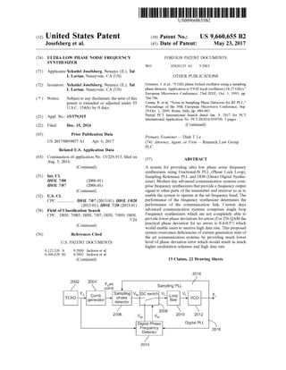
  • 1. (12) United States Patent Josefsberg et al. USOO9660655B2 US 9,660,655 B2 May 23, 2017 (10) Patent No.: (45) Date of Patent: (54) ULTRA LOW PHASE NOISE FREQUENCY SYNTHESIZER (71) Applicants:Yekutiel Josefsberg, Netanya (IL); Tal I. Lavian, Sunnyvale, CA (US) (72) Inventors: Yekutiel Josefsberg, Netanya (IL); Tal I. Lavian, Sunnyvale, CA (US) Notice:(*) Subject to any disclaimer, the term ofthis patent is extended or adjusted under 35 U.S.C. 154(b) by 0 days. (21) (22) Appl. No.: 15/379,915 Filed: Dec. 15, 2016 (65) Prior Publication Data US 2017/OO99057 A1 Apr. 6, 2017 Related U.S. Application Data Continuation ofapplication No. 15/229.915, filed on Aug. 5, 2016. (63) (Continued) Int. C. HO3L 7/08 HO3L 7/07 (51) (2006.01) (2006.01) (Continued) (52) U.S. Cl. CPC ................ H03L 7/07 (2013.01); H03L I/028 (2013.01); H03L 7/20 (2013.01) Field of Classification Search CPC. H03L 7/085; H03L 7/07; H03L 7/099: H03L 7/24 (58) (Continued) (56) References Cited U.S. PATENT DOCUMENTS 9/2000 Jackson et al. 4/2002 Jackson et al. 6,122,326 A 6,366,620 B1 FOREIGN PATENT DOCUMENTS WO O3O26133 A1 3,2003 OTHER PUBLICATIONS Gismero, J. et al., “9 GHZ phase locked oscillator using a sampling phase detector. Application to VSAT local oscillators(18-27GHz).” European Microwave Conference, 23rd IEEE, Oct. 1, 1993, pp. T84-786. Liman, R. et al., “Noise in Sampling Phase Detectors for RF PLL.” Proceedings of the 39th European Microwave Conference, Sep. 29-Oct. 1, 2009, Rome, Italy, pp. 480-483. Partial PCT International Search dated Jan. 9, 2017 for PCT International Application No. PCT/IB2016/054790, 3 pages. (Continued) Primary Examiner — Dinh T Le (74) Attorney, Agent, or Firm — Remarck Law Group PLC (57) ABSTRACT A system for providing ultra low phase noise frequency synthesizers using Fractional-N PLL (Phase Lock Loop), Sampling Reference PLL and DDS (Direct Digital Synthe sizer). Modern day advanced communication systems com prise frequency synthesizers thatprovide a frequency output signal to other parts ofthe transmitter and receiver so as to enable the system to operate at the set frequency band. The performance of the frequency synthesizer determines the performance of the communication link. Current days advanced communication systems comprises single loop Frequency synthesizers which are not completely able to provide lowerphase deviations for errors (For256 QAM the practical phase deviation for no errors is 0.4-0.5°) which would enable users to receive high data rate. This proposed system overcomes deficiencies ofcurrent generation state of the art communication systems by providing much lower level ofphase deviation error which would result in much higher modulation schemes and high data rate. (Continued) 13 Claims, 22 Drawing Sheets 2016 2992 2004 Fas c ( Y comb Sanging Pii. F. w Sanging Wis DC switch W WCor: s loop 't F,CXC phase -- - WCO generator detector w fier 'N A 208 i8 Vs 21 2O bigital Digital Pt. Frequency Detectic? O18 2014
  • 2. US 9,660,655 B2 Page 2 Related U.S. Application Data (60) Provisional application No. 62/181,221, filed on Jun. 18, 2015. (51) Int. Cl. HO3L 7/20 (2006.01) HO3L I/02 (2006.01) (58) Field of Classification Search USPC .................................................. 327/1.47 159 See application file for complete search history. (56) References Cited U.S. PATENT DOCUMENTS 7.391,839 B2 * 6/2008 Thompson ................ HO3L 7/16 327,156 7,545,224 B2 * 6/2009 Chow ....................... HO3L 7/10 33 1/16 7,656,236 B2 * 2/2010 Williams ................ HO3L 7,087 331f1 R 8,378,751 B2 2/2013 Fagg 8,704,562 B2 4/2014 Nicholls et al. 8,816,777 B2 * 8/2014 Szilagyi .................... HO3L 7/08 327,156 OTHER PUBLICATIONS Teng, K.H. et al., “Microwave Phase-Locked Loop Circuit Devel opment and Efficiency Improvement.” IEEE, High Frequency Post graduate Student Colloquium, Sep. 8 and 9, 2003, pp. 128-131. U.S. Appl. No. 15/229.915, filed Aug. 5, 2016, Josefsberg et al. U.S. Appl. No. 15/379,860, filed Dec. 15, 2016, Josefsberg et al. * cited by examiner
  • 3. U.S. Patent May 23, 2017 Sheet 1 of 22 US 9,660,655 B2 2O2 2O4. 28 28 Sf Contro FG. 2
  • 4. U.S. Patent May 23, 2017 Sheet 2 of 22 US 9,660,655 B2 300N 3O4. FG. 3 FG. 4
  • 5. U.S. Patent May 23, 2017 Sheet 3 of 22 US 9,660,655 B2 50 N SO 334 O-MC S A s A2 : INPUT C. OU NP CH O y r SAVE SAf CON rC M/ CONTRO FG. 5 ERROR WOAGE O
  • 6. U.S. Patent May 23, 2017 Sheet 4 of 22 US 9,660,655 B2 s - O O
  • 7. US 9,660,655 B2Sheet S of 22May 23, 2017U.S. Patent N-DECISION SONARY O O O FG. 8
  • 8. U.S. Patent May 23, 2017 Sheet 6 of 22 US 9,660,655 B2 9OO N Free-Running WCO Phase Noise -Shaped WCQ ( Phase Noise loop f Eadwict F.G. O
  • 9. U.S. Patent May 23, 2017 Sheet 7 of 22 US 9,660,655 B2 Noise die -100 O2 -oneOscillator-wg v -WCO * w w phase Comparator frequency divider VCO, resistor of PF afterPLLresponse phase COrgaratof CO3 Baldwidth frequency divider Cop Badw afterPresponse Offset Frequency (hiz} easured Piase Noise 10 102 103 04 105 106 Offset Frequency (Hz) FG 11
  • 10. U.S. Patent May 23, 2017 Sheet 8 of 22 US 9,660,655 B2 1200- --Carrier i-band phase noise Noise peaking due to 1.loop transfer fiction - intere?ty phase noise 20 log(N) : Synthesizer phase N-N2 noise floor F.G. 12 1300 PS Single Sidebad phase dB noise Pss 1-2 3 Single sideband phase noise FG. 3
  • 11. U.S. Patent May 23, 2017 Sheet 9 of 22 US 9,660,655 B2 1400 15CO Y 5O2 1504 SO6 Fas ing Of Corb Sampi phas detect F.cit
  • 12. U.S. Patent May 23, 2017 Sheet 10 of 22 US 9,660,655 B2 18O N 1606 1808 MPSE RAN GENERATOR SORCE 2 to 2 4 6 is 2022 24 2s 28 go 33 34 g6 38 40 Frequency (Giz) F.G. 17
  • 13. U.S. Patent May 23, 2017 Sheet 11 of 22 US 9,660,655 B2 1800 outina 1824 1822 F.G. 18 1900 94. ...... -/3O2 Fractionai-N 9 O 914 tiina - - - - - - - - - - - - - Sanping P.
  • 14. US 9,660,655 B2Sheet 12 of 22May 23, 2017U.S. Patent {}{}{}?
  • 15. U.S. Patent May 23, 2017 Sheet 13 of 22 US 9,660,655 B2 s & 2-foop SON Sw-d CN: r ev;
  • 16. US 9,660,655 B2Sheet 14 of 22May 23, 2017U.S. Patent ZZ"SO|-
  • 17. US 9,660,655 B2Sheet 15 of 22May 23, 2017U.S. Patent 3SON. 8Se.z-pop
  • 18. US 9,660,655 B2Sheet 16 of 22May 23, 2017U.S. Patent ----- z-pop 8sion 8Seid
  • 19. US 9,660,655 B2Sheet 17 of 22May 23, 2017U.S. Patent z-pop as on 8Setic
  • 20. US 9,660,655 B2Sheet 18 of 22May 23, 2017U.S. Patent zip3p 8sion ased g-rC c N
  • 21. US 9,660,655 B2Sheet 19 of 22May 23, 2017U.S. Patent zijapasoNased
  • 22. US 9,660,655 B2Sheet 20 of 22May 23, 2017U.S. Patent
  • 23. US 9,660,655 B2Sheet 21 of 22May 23, 2017U.S. Patent 9053 ^oosz
  • 24. U.S. Patent May 23, 2017 Sheet 22 of 22 US 9,660,655 B2 ATCXO generates clock signals of low noise frequency ranges 00 V-2 to 250 V-2 -3002 A Sampling Phase Detector receives the 304 clock signals and eliminate digital noise floor present in the incoming clock signals A Digital Pit is added with the Sampling P. to improve performance and reliability of an itra low Phase Noise -3006 Frequency Synthesizer to achieve high data rates, high modulation schemes and ow phase deviatioi errors. Ec FG. 3O
  • 25. US 9,660,655 B2 1. ULTRA LOW PHASE NOISE FREQUENCY SYNTHESIZER CROSS-REFERENCE TO RELATED APPLICATIONS This application is a continuation ofU.S. application Ser. No. 15/229,915, filed Aug. 5, 2016, which claims priority to U.S. Provisional PatentApplication No. 62/181,221 filed on Jun. 18, 2015. The entire disclosure of each of the above applications is incorporated herein by reference. FIELD Embodiments of the present disclosure is generally related to systems to provide ultra low phase noise fre quency synthesizer and in particular relate to systems to provide ultra low phase noise frequency synthesizer based on using combination of Fractional-N PLL (Phase Lock Loop), Sampling Reference PLL and DDS (Direct Digital Synthesizer). BACKGROUND Wireless Communication Technologies have completely revolutionized how millions ofpeoples in today’s world are communicating to each other in a seamless manner. From theirearly infant days oflate 1800's till today the concept of wireless communications have matured beyond our wildest imaginations. Amongst all those technological advances related to the field ofwireless communication technologies, the only thing which has remained constant is the applica tion of radio waves. On one hand radio waves can help us achieve communication between people who are located in close proximity offew meters. In the same manner in deep space radio communications those same radio waves can also help us achieve crystal clear communication between humans who are millions of kilometers away from each other. Wireless Communication Technologies have branched into multiple different formats like Two-Way Radio Com munications, Satellite Communications, Infrared Commu nications, Mobile Communications, Microwave Communi cations, Wireless Data Communications, Wi-Fi, Bluetooth Technology etc. Each and every single one of the above disclosed wireless communication technologies have evolved tremendously andbecome much more Sophisticated and state of the art. In this patent application we will specifically deal with systems associated with Mobile Com munications. The evolution of mobile communication technologies from their initial 1G (1 Generation) days of 1970 till 2016 which is today's high speed 4G (4 Generation) technologies haveenriched human lives in different shapes and sizes. The biggest impact which these gradual evolutions of mobile communication technologies have brought into our lives is the humongous increase in data speed which has enabled seamless communications between millions of peoples. Where 1G technology enabledcommunication systems used to provide us simple Voice communications at only 10Kbps data rate, the theoretical download data rate of the most advanced mobile communication technologies as of 2016 which is LTE-Advanced (Long Term Evolution) has been proposedas 1 Gbps. This quantumjump in data rate from 10 Kbps to 1 Gbps has left tremendous impact into common peoples lives. 10 15 25 30 35 40 45 50 55 60 65 2 Without the availability of the advanced state of the art communication systems in today's markets like Smart phones, it is not at all possible to access those high speed data rates. One of the most important hardware element present in those state of the art systems like Smart phones, are frequency synthesizers. Frequency Synthesizers are a major building block in almost every communication sys tems, such as advanced mobile communication systems (LTE, LTE-Advanced), satellite communication systems, radar communication systems and so on. An example frequency synthesizer provides a frequency output signal to otherparts ofthe transmitterand receiver So as to enable the system to operate at the set frequency band. The performance of the frequency synthesizer determines the performance of the communication link. The main important features of every synthesizer are: a) Output fre quency range, b) Output frequency resolution, c) Switching speed between channels and d) Spectral purity: Phase noise, spurious and harmonics etc. Amongst all those above men tioned features phase noise is the most important. The level of phase noise determines the modulation scheme that can be implemented in the system hardware and thus it deter mines the associated data rates and the communication ranges of the systems. Ifa communication system provides higher data rate the system is more efficient, and it takes less time to download and upload data from the network. Ahigherdatatransferrate can even save battery time because the transmission can be turned off much faster. A higher order modulation scheme implemented in the State ofthe art communication systems enables those systems to push more information in the wireless channels. However, the modulation scheme is lim ited by phase noise. Hence to implement those higher modulation schemes in the existing state ofthe art commu nication systems we need to reduce the phase noise. Most modern communication systems use Sophisticated modulation schemes that are based on a combination of different phases and amplitudes. The current most advanced modulation scheme which is running in most of the Smart phones or tablets is 256 QAM (256 Quadrature Amplitude Modulation). In this modulation Scheme, the Smallest phase deviation for error (Ap) theoretically is 3.7°. Practically, to be on the safe side, it is desired to work with nicely lower number. As 10% is considered safe, hence the current generation of frequency synthesizers work with 0.4°-0.5°. Thecurrentgeneration ofsingle loop frequency synthesizers inherently does not enable to go to much lower phase error due to phase noise. The current generation ofadvanced state of the art com munication systems typically includes a front end module and a System on Chip (SoC). The frequency synthesizer is part ofthe SoC and is implemented mostly in CMOS. The front end module usually contains a low noise amplifier for the receiver, the power amplifier for the transmitter and some switch matrix. The SoC includes all the signal pro cessing elements along with the frequency synthesizers. Currently the Wi-Fi and/or LTE synthesizers in the SoC set the limit for the performance ofthe system. As a result, the multi-billion dollar market remains at a technological stand still. Further, in many communication systems, Digital Pre Distortion (DPD) is an algorithm that aims to pre-distort transmitted signals in orderto improve linearity. In practical terms, it means that the transmitter is not completely linear and is distorting the signal. And that basically also prevents the system to be as effective as much as possible. So one approach is to correct it is by using some algorithms to pre
  • 26. US 9,660,655 B2 3 distort the signal in the opposite way. To do this efficiently, the DPD algorithm requires the amplitude and phase data about the transmitted data. Traditional radio systems either utilize the receive path of the radio ora special down-conversion mechanism followed by a high-resolution analog to digital converter to capture the small non-linearities of the transmit path. The main problem with the above mechanism is that non-linearities and phase noise of the receive path or special down conversion path get added to the signal and the DPD algorithm cannot separate the non-linearities and the phase noise generatedand addedduringthe down-conversion from the ones that were actually created in the transmit path and need correction. The transmit path nonlinearities; can come from any component such as low frequency amplifier, mixer, up converter, driver amplifier. Specifically the PowerAmplifier (PA) is the main source of nonlinear distortions in the transmit path and the main goal ofthe DPD algorithm is to pre-distort this to achieve a cleaner signal. As mentioned above all the receive path nonlinearities are added to the transmit path with no way to distinguish between the two. Hence, there is a need for a low phase noise frequency synthesizer that can overcome the problems of prior art, enable higher modulation schemes and high data rate by reducing phase noise, resolve the locking problem in the sampling PLLs and minimize DPD distortions in received signals. The target of the present disclosure is to enable much lower level of phase deviation for error (Ae) which should be in the range of 10% ofcurrent designs, or 0.04° andthusenables much higherordermodulation schemes and enables an efficient DPD algorithm. SUMMARY The present disclosure is discussed in reference to stateof the art wireless communication systems (Smartphones) for exemplary purposes only. It is contemplated that the present disclosure is applicable to any state of the art wireless communication systems which enables consumers to com municate with each other in a seamless manner. According to a first embodiment ofthe present disclosure a system comprising one ultra low phase noise frequency synthesizer is provided. The system is made up with a front end module, a display screen and one System on Chip (SoC) module. The ultra low phase noise frequency synthesizer is partoftheSoC module. Theultra low phase noise frequency synthesizercomprises one main PLL(Phase Lock Loop) and one reference sampling PLL. The main PLL comprises one high frequency DDS (Direct Digital Synthesizer), one Digi tal Phase Frequency Detector, one main VCO (Voltage Controlled Oscillator), one frequency dividerand one down convert mixer. The reference sampling PLL comprises one TCXO (Temperature Compensated Crystal Oscillator), one sampling phase detector, and one reference VCO. This embodiment provides multiple improvements in System output which are based on the following technical approaches—a) using of dual loop approach to reduce frequency multiplication number, b) using ofsampling PLL as the reference PLL to make its noise contribution negli gible, c) using ofDDS to providehigh frequency input to the main PLL and d) using of high frequency Digital Phase Frequency Detector in the main PLL. According to a second embodiment ofthe present disclo Sure a system comprising one ultra low phase noise fre quency synthesizer is provided. The system is made up with afrontend module,adisplay Screenand one System onChip 5 10 15 25 30 35 40 45 50 55 60 65 4 (SoC) module. The ultra low phase noise frequency synthe sizer is part ofthe SoC module. The ultra low phase noise frequency synthesizercomprises one main PLL (Phase Lock Loop) and one reference sampling PLL. The ultra low phase noise frequency synthesizer comprises one single TCXO (Temperature Compensated Crystal Oscillator) which pro vides input clock signals to both the main PLL and the reference sampling PLL. The main PLL further comprises one Fractional-N Synthesizer chip, one primary VCO (Volt age Controlled Oscillator)and one down convert mixer. The Fractional-N Synthesizer chip includes one Digital Phase Detector and one software controllable variable frequency divider. The reference sampling PLL comprises one sam pling PLL, and one reference VCO. This embodiment pro vides multiple improvements in system output which are based on the following technical approaches—a) using of dual loop approach to reduce frequency multiplication num ber, b) using ofsampling PLLto make its noise contribution negligible, c) instead ofa DDS clock like in the previous embodiment, using of a high frequency TCXO clock to provide high frequency input to the main PLL, and d) using of a high frequency Fractional-N Synthesizer chip in the main PLL. Accordingtoathirdembodiment ofthepresentdisclosure a system comprising one ultra low phase noise frequency synthesizer is provided. The system is made up with a front end module, a display screen and one System on Chip (SoC) module. The ultra low phase noise frequency synthesizer is partoftheSoC module. The system comprises one sampling PLL (Phase Lock Loop), which is one ofthe most important building blocks of an ultra low phase noise frequency synthesizer. The sampling PLLcomprises one TCXO (Tem perature Compensated Crystal Oscillator), one Comb Gen erator, one Sampling Phase Detector, one DC Switch, one Loop Filter, one VCO (Voltage Controlled Oscillator) and one Digital Synthesizer. In this embodiment, the loop filter is just a loop filter. The Digital Synthesizer acts as a phase detectorwhen the loop is locked and as a frequency detector when the loop is open, forcing the loop to lock from any distance between the two frequencies. The loop will lockby the Digital Synthesizer. Once it is locked, the lock indicator will switch the PLL to the sampling PLL while keeping the same control Voltage, thus keeping the loop locked. The preceding is a simplified Summary to provide an understanding ofSome aspects ofembodiments ofthe pres ent disclosure. This Summary is neither an extensive nor exhaustive overview ofthepresent disclosureandits various embodiments. The Summary presents selected concepts of the embodiments of the present disclosure in a simplified form as an introduction to the more detailed description presentedbelow. As will be appreciated, otherembodiments of the present disclosure are possible utilizing, alone or in combination, one or more ofthe features set forth above or described in detail below. BRIEF DESCRIPTION OF THE DRAWINGS The above and still further features and advantages of embodiments ofthe present invention will become apparent upon consideration of the following detailed description of embodiments thereof, especially when taken in conjunction with the accompanying drawings, and wherein: FIG. 1 illustrates a general block diagram of a negative feedback system; FIG. 2 illustrates a general block diagram of a standard Phase Lock Loop (PLL);
  • 27. US 9,660,655 B2 5 FIG. 3 illustrates a simplified drawing ofa digital phase/ frequency detector; FIG. 4 illustrates an example ofan active filter as applied to a general PLL; FIG. 5 illustrates the principleofsample-and-hold mecha nism; FIG. 6 illustrates a schematic ofthe step recovery diode as comb generator feeding the dual Schottky diode that acts as phase detector; FIG. 7 illustrates a complete example schematic of the comb generator and sampling phase detector with RF pre amplifier and two DC buffers following the phase detector; FIG. 8 illustrates a 64 QAM modulation scheme used in communication equipment; FIG. 9 illustrates a phase noise plot of an example free running Voltage Control Oscillator (VCO) in the frequency domain (spectrum analyzer), without being locked in a PLL; FIG. 10 illustrates a phase noise plot of an example Voltage Control Oscillator (VCO) in the frequency domain (spectrumanalyzer), compensated by being locked ina PLL; FIG. 11 illustrates two plots: (a) a simulation of phase noise ofan example PLL, and (b) is an actual measurement; FIG. 12 illustratesaphase noiseplotofa closed loop PLL, showing clearly the effect ofthe phase detector multiplica tion number 20*LOG(N) within loop bandwidth: FIG. 13 illustrates a plot ofmeasurement terms ofphase noise in 1 Hz bandwidth at a Afoffset frequency from the carrier. FIG. 14 illustrates a general block diagram ofan example dual loop PLL; FIG. 15 illustrates a general block diagram ofan example dual sampling PLL; FIG. 16 illustrates how impulse or “comb' generator changes a wave shape ofa signal from sine wave to pulses; FIG. 17 illustrates an example outputofa comb generator in the frequency domain; FIG. 18 illustrates a block diagram ofan ultra-low phase noise frequency synthesizer as suggested in a first embodi ment, FIG. 19 illustrates a block diagram ofan ultra-low phase noise frequency synthesizer as Suggested in a second embodiment; FIG. 20 illustrates a block diagram ofthe sampling PLL system as suggested in a third embodiment; FIG. 21 illustrates a phase noise simulation plot contrib uted by a DDS chip in accordance with the first embodiment of the present disclosure; FIG. 22 illustrates a phase noise simulation plot contrib uted by a main PLL in accordance with the first embodiment of the present disclosure; FIG. 23 illustrates a phase noise simulation plot contrib uted by a reference sampling PLL having the TCXO clock generating input frequenciesof100MHz in accordance with the first embodiment ofthe present disclosure; FIG. 24 illustrates a phase noise simulation plot contrib uted by a reference sampling PLL having the TCXO clock generating input frequenciesof250MHz in accordance with the first embodiment ofthe present disclosure; FIG. 25 illustrates a phase noise simulation plot contrib uted by a main PLL in accordance with the second embodi ment ofthe present disclosure; FIG. 26 illustrates a phase noise simulation plot contrib uted by a reference sampling PLL having the TCXO clock generating input frequenciesof100MHz in accordance with the second embodiment of the present disclosure; FIG. 27 illustrates a phase noise simulation plot contrib uted by a reference sampling PLL having the TCXO clock 10 15 25 30 35 40 45 50 55 60 65 6 generating input frequencies of250MHz in accordance with the second embodiment of the present disclosure; FIG. 28 illustrates a flow chart depicting the operational method steps ofthe first embodiment; FIG. 29 illustrates a flow chart depicting the operational method steps ofthe second embodiment; and FIG. 30 illustrates a flow chart depicting the operational method steps ofthe third embodiment. To facilitate understanding, like reference numerals have been used, where possible, to designate like elements com mon to the figures. DETAILED DESCRIPTION As used throughout this application, the word “may is used in a permissive sense (i.e., meaning having the poten tial to), ratherthan the mandatory sense (i.e., meaning must). Similarly, the words “include”, “including', and “includes’ mean including but not limited to. The phrases “at least one”, “one or more', and “and/or are open-ended expressions that are both conjunctive and disjunctive in operation. For example, each of the expres sions “at least one ofA, B and C', 'at least one ofA, B, or C”, “one or more ofA, B, and C. “one or more ofA, B, or C” and "A, B, and/or C' means A alone, B alone, C alone, Aand B together, Aand C together, B and C together, orA, B and C together. The term “a” or “an entity refers to one or more ofthat entity. As such, the terms “a” (or “an”), “one or more' and “at least one' can be used interchangeably herein. It is also to be noted that the terms “comprising”, “including, and “having can be used interchangeably. The term “automatic' and variations thereof, as used herein, refers to any process or operation done without material human input when the process or operation is performed. However, a process or operation can be auto matic, even though performance ofthe process or operation uses material or immaterial human input, if the input is received before performance of the process or operation. Human input is deemed to be material if such input influ ences how the process or operation will be performed. Human inputthat consents to theperformance ofthe process or operation is not deemed to be “material'. FIG. 1 illustrates a general block diagram of a negative feedback system 100. The negative feedback system 100 has an input R and an outputC,aSummer/comparator102,aforwardpath function G 104 and a feedback path function H 106. The summer/ comparator 102 compares the input Rwith a sample B ofthe output C fed back through function H 106, to produce an error signal E that is relative to the difference between the input Rand the feedback sample B. This errorsignal E is fed to the main element G function 104 in the forward path. If the output signal C tends to drift upwards, the error signal E pushes it back downwards and vice versa. Thus, the negative feedback system 100 stabilizes the output signal C. The negative feedback system 100 finds applications in many systems for stabilizing frequency, output power, and many other functions. FIG. 2 illustrates a general block diagram of a standard Phase Lock Loop (PLL) 200. The PLL 200 is a frequency feedback system comprising a reference clock 202, a digital phase/frequency detector (PFD) 204, a loop filter 206, a VoltageControlled Oscillator (VCO) 208, and a frequency divider 210. The VCO 208 is the main output block in the forward path, and is tuned to produce a frequency as set by a tuned
  • 28. US 9,660,655 B2 7 circuit.TheVCO 208 has a frequency output F thatcan be changed by a control voltage V, over a pre-set range of frequencies. The phase detector 204 is a comparator forboth the clock input F and the feedback sample from the output F. divided by divider N210. The phase detector 204 compares the two input frequencies F and F/N. When the two input frequencies are not equal, the device 204 acts as a frequency discriminator and produces either a negative or positive Voltage, depending on the polarity ofthe frequency difference between the two inputs. When the two input frequencies are the device produces an error Voltage V, relative to the phase difference between the two equal frequencies. The loop filter 206 filters and integrates the error signal produced by the phase detector 204 and feeds it to the VCO 208. The loop filter 206 is usually based on passive com ponents like resistors and capacitors, but also in some cases it is a combination ofactive devices like operational ampli fier and passive components. The reference clock 202 is in general a low frequency crystal oscillator signal source that feeds F to the phase detector204,and to which theoutputsignal F is “locked'. The reference clock 202 is set at some frequency for example a standard frequency 10 MHz.The locking “mecha nism' transfers some ofthe qualities ofthe reference clock 202 to the main output signal F. Its main features usually are: a) frequency stability over temperature generally in the rangeof0.1-5 ppm (parts permillion),b)accuracy—Can be tuned to very high accuracy, c) very low phase noise—Its phase noise is transferred to the output signal multiplied by the ratio of 20*LOG(N) where N is the ratio between the output frequency and the clock frequency applied to the phase detector 204. The frequency divider 210 is based on digital devices like gates and flip-flops, through which the input frequency F. is divided by a number N to produce F/N which is fed to the other input ofthe phase detector 204. This number N is Software controllable. The control signal comes usually from a micro controller or from a PC or from anywhere that basically will send software control to the frequency divider 210 to change the division number N. The target of the division number N is to enable the output frequency ofthe frequency divider 210 to be equal to the clock frequency of the reference clock 202. The entire operational procedures of a standard Phase Lock Loop (PLL) 200 is as follows: Ifan input clock signal F is applied, usually by a reference clock202, the phase detector 204 compares the phase and frequency ofthe input signal F with that of the VCO 208 divided by N, and generates an error voltage V, that is related to the difference in the two signals. The error voltage V, is then filtered and applied to the control ofthe VCO 208, thereby varying the VCO 208 frequency in a direction that reduces the frequency difference between thetwo signals. When the frequencies of the two signals become sufficiently close, the feedback nature of the system causes the system to lock with the incoming signal. Once in lock the VCO 208 frequency divided by N is identical with the input signal F, except for a finite phase difference which is necessary to generate the corrective error voltage V, to shift the VCO 208 fre quency to the input signal frequency F thus keeping the system in lock. Any time, the division number N is changed, say for example by 1, the output frequency F. jumps exactly by a step. In an example, if the reference clock 202 generates a ciocic 5 10 15 25 30 35 40 45 50 55 60 65 8 frequency 1 MHz, then every time the division number N changes by steps of 1, the output frequency F changes by equal steps of 1 MHz. Like all negative feedback systems, the PLL 200 has a loop bandwidth set by the component parameters and the loop filter206. In otherwords, the PLL200 is a sophisticated frequency multiplier with a built-in narrowband, automati cally tuned band-pass filter as the output frequency F is basically F multiplied by the number N. The loop bandwidth is also responsible directly for how fast the output frequency ofPLL 200 may change between different frequencies. The PLL 200 is a device where the VCO 208 is locked to a single clock reference signal which is very low but also very clean and very stable and the output frequency can be changed by equivalent steps by controlling the frequency divider 210 in the feedback loop. FIG. 3 illustrates a simplified drawing ofa digital phase/ frequency detector 204. A phase detector or phase comparator is a frequency mixer, analog multiplier or logic circuit that generates a Voltage signal which represents the difference in phase between two signal inputs. It is an essential element ofthe phase-locked loop (PLL). A specialized variant that addi tionally detects frequency is referred as Phase Frequency Detector (PFD). Aphase-frequency detector is an asynchro nous sequential logic circuit which determines which ofthe two signals has a Zero-crossing earlier or more often. When used in a PLL application, lock can be achieved even when it is off frequency. Such a detector has the advantage of producing an output even when the two signals being compared differ not only in phase but in frequency. The phase/frequency detector 204 compares two input frequencies F and F/N. When the two input frequen cies are not equal, it acts as a frequency detector and produces one or Zeros to produce a Voltage control V, that pushes corresponding VCO 208 in the direction of the reference. In other words, if the VCO 208 is above the reference then the voltagecontrolV, is high topush theVCO 208 down and vice versa. When the two input frequencies are the same and a frequency lock is achieved, the phase detector 204 acts as a phase detector and compares the two phases, and continues to produce an error Voltage to control the frequency and phase ofthe output device. FIG. 4 illustrates an example ofan active filter as applied to a general PLL 400. The kind ofloop filteri.e. passive filteroractive filtercan be chosen on the basis of specific requirement. A passive loop filteris based on resistors and capacitors only, while an active loop filter is based on an amplifier and a capacitor resistor network in the feedback system. A passive filter is preferred in cases where, a reference PLL is of a single frequencyand will need only a single Voltage in orderto stay in that single frequency. The other reasons being simplicity, costand mostadvantageously no addition ofnoise, as active devices tend to add additional noise in thesystem. However, active filters find more acceptances because ofthe possibil ity of amplification of the input signal. Amplification is made possible by an operational amplifier employed in the active filter. The loop filter 206 of FIG. 2, is an active filter that includes an operational amplifier 402 and a capacitor-resis tor network 404 in the feedback loop. In some instances, the phase detector 204 ofthe PLL 200 may produce voltage up to 5 volts but the corresponding VCO 208 may need a voltage ofabove 5 volts, say, forexample, up to 18 volts in data
  • 29. US 9,660,655 B2 order to reach its complete range, so the active filter 206 facilitates not only filtering but also provides the capability to go to higher Voltages. FIG. 5 illustrates the principleofsample-and-hold mecha nism 500. The first sample and hold circuit 502 includes a switch S and a hold capacitor C. The operation of the Switch S is controlled by the sample control. When the switch S is closed, a Voltage sample ofthe input frequency is sampled and when the Switch is opened,the Voltagesampleis held on the hold capacitor C. The second sample and hold circuit 504 includes two buffers A1 and A2 with unity gain for isolation purposes, in addition to the switch S and the hold capacitor C. The buffer A2 is preferably an electronic buffer, so that the hold capacitor C does not discharge parasitically between con secutive samples. In other words, the hold capacitor C. holds the Voltage between samples. FIG. 6 illustrates an example ofpractical implementation of a comb generator and sampling phase detector. The schematic shows a Step Recovery Diode (SRD) as comb generator feeding the dual Schottky diode that acts as phase detector. The implementation circuit 600 including a Step Recov ery Diode (SRD) 602 as a comb generator and the dual schottky diodes 604 and 606 as a phase detector. The input to thecircuit 600 in thisexample is a clockinput of 100 MHz sine wave. The SRD 602 is a special device that turns the 100 MHz sine wave input into a very narrow pulse train ofthe same frequency, so it acts as a comb generator. The two schottky diodes 604, 606 act as switches and act as sampling switches. The RF voltage (output from corre sponding VCO) to be sampled is connected to a point between the two diodes 604 and 606. The SRD 602 creates an output ofpositive and negative pulses. The positive and negative pulses act as control signals to the diodes 604 and 606 that act like switches. The sampled voltage output is an error DC voltage which is created by sampling the RF input through the dual schottky diodes 604 and 606. The output of the RF signal is sampled whenever the diodes 604 and 606 are opened by the narrow pulses coming from the SRD 602. The voltage sampleis held on thecapacitors C following the diodes 604 and 606. FIG. 700 illustratesa schematic ofthecombgeneratorand sampling phase detector with a clock pre-amplifier and two DC buffers following the phase detector. TheVoltagesamplesareheld ontwo very Small capacitors (which are basically the input capacitance of the Voltage buffers, no need for external capacitors) on both sides ofthe dual diode pair, so as not to enable the whole capacitor to discharge parasitically between the samples. These capaci tors are buffered by a couple ofultra-low input bias current buffers to prevent discharge between samples. The two voltages are summed, fed to a loop filter, whereby the clean V, is fed to the VCO to control the frequency. This implementation of Sampling phase detector creates an analogphase detector, very similar to a mixer. The analog sampling phase detector has a certain defined locking space orlocking distance, and it does not lock from any frequency difference like the phase/frequency digital detector. It has Some locking range and only within that locking range, the VCO locksby itselfon the reference. In a sampling PLL, the VCO does not lock on the reference, but on the Nth harmonic ofthe reference. In other words, one can lock a 9 GHzon the 90th harmonic ofthe 100 Megahertzclock. This is done as the input frequency is sampled every 100 cycles, not every cycle. 10 15 25 30 35 40 45 50 55 60 65 10 This type of product may contain some “search mecha nism' to help lockthe PLL. The mostcommon one involves a positive feedback on the loop filter itself. While the loop is not locked, the loop filter acts as a very low frequency oscillator that drives the VCO back and forth across the frequency range. When it passes close enough to the har monic of the clock, it will lock and stay locked. A nice feature ofthis mechanism is that it turns off automatically when the loop locks. This happens because ofthe nature of the loop as a negative feedback system. However, this type of search mechanism suffers from many problems, its operation is subject to temperature changes and it makes this product difficult to produce, tune and sell Successfully. FIG. 800 illustrates a 64 QAM modulation scheme used in communication equipment. Communication equipment, including different Smart phones or tablets use a modulation scheme called Quadra ture Amplitude Modulation (QAM). The QAM number defines the amount ofpoints on a 2 dimensional chart that that isalways the sizeof1x1.The more points, the largerthe density ofthe points. The signal has to be very clean for the points tobeexactly wherethey are supposed to beso thatthe modem can decide easily. Phase noise is one of the bottle necksthat limitthe datathroughput. At a system level, phase noise isastatisticalparameterthat movesa modulationpoint along a curvejust as a vector would move ifit power would stay the same but the angle changes. Ifa certain modulation point moves too much on this curve, the modem will have a difficult time deciding where this point belongs and will flag an error. In the QAM, delta (p or delta phase is the maximum error in degrees that is allowed to demodulate the data correctly. Ifthepoint movesby a phaseofdelta (p, itwill be understood as a different point and in time the modulation scheme of course will have lot oferrors. The 256 QAM allows a phase error ofapproximately 3 degrees in order to understand the data and the 64 QAM allows a phase errorofapproximately 7 degrees. By getting a better angle between 2 Separate signals, one can achieve a much better more information per HZ, and a much higher data rate in modulation schemes, which can be very beneficial in many ways even improving battery life. With our proposed ultra-low phase noise frequency syn thesizers, the improved phase noise translated to degrees is better than 0.04 degrees, which when basically translated to modulation scheme can facilitate much higher modulation range. In other words, the points on the graph 800 can be much more crowded because there would be much more points in higher modulation level. The points may be much more crowdedbutifthe phase noise is much better, it would be easy to distinguish between them without having prob lems ofphase noise. With better phase noise, one may be able to push more information perHz. On the samechannel, one can get more information encoded and decoded. And basically it means that one can get better data rate. FIG. 9 illustrates a phase noise plot 900 of an example free running Voltage Control Oscillator (VCO) in the fre quency domain (spectrum analyzer), withoutbeing locked in a PLL. As said before, Phase noise is a key element in many RF and radio communications systems as it can significantly affect the performance of systems. Phase noise is the fre quency domain representation ofrapid, short-term, random fluctuations in the phase of a waveform, caused by time domain instabilities also referred to as "jitter.
  • 30. US 9,660,655 B2 11 For example, in frequency domain, where the scales are amplitude vs. frequency, ideally a frequency of 100 MHz may look like a single line staying at exactly 100 MHz. However, practically with modern equipment in the labora tory, amplitude VS frequency may not look like a single line but it will look like a single line with a “skirt” 902 which goes wider and wider as we go down. The phase noise plot 900 looks like the skirt 902 on the left and the right of the exact desired frequency f. The quality, height, width ofthe skirt 902 determines how the phase noise may affect the system or the performance ofthe system. So, it is desirable to minimize phase noise as much as possible is to improve the system performance. Phase noise is another term to describe short-term fre quency stability. The signal generated by a frequency source is neverpractically“clean'. Its frequency is neverabsolutely stable at the desired value. It has "Phase Noise' which is frequency shifting, i.e. Small frequency shifts at different rates and different amplitudes of the main frequency. It changes around the center set frequency fat different rates and amplitudes. In time domain, the phase noise may be referred to as jitter. Long term frequency stability is drift of the center frequency over time or over temperature. FIG. 10 illustrates a phase noise plot 1000 ofan example Voltage Control Oscillator (VCO) in the frequency domain (spectrum analyzer), compensatedby being locked in a PLL. The upper line 1004 is the free running VCO phase noise, before it is locked in a PLL, and the lower line 1002 is the shaped VCO phase noise. In the PLL, the principle of locking the VCO to a reference frequency attenuates the phase noise of the VCO, in an amount related to the loop bandwidth. Outside the loop bandwidth, the VCO noise remains almost same as the phase noise without the PLL. while inside loop bandwidth it is attenuated more and more as offset frequency from the main carrieris reduced. At very high frequency, i.e. above the loop bandwidth, the locking almost has no effect, as the phase detector correction signal is not fast enough to reach the VCO for very fastchanges or very fast disturbances. However, inside the loop bandwidth or at low frequencies, the compensated phase noise of the VCO is much lower than that ofthe free running VCO. All the frequencies that is close to the center ofthe frequency f. are easy to detect and compensate. FIG. 11 illustrates two plots 1100: (a) a simulation of phase noise ofan example PLL, and (b) an actual measure ment. FIG.11(a) illustrates a simulation graph ofphase noiseof an example PLL. The simulation graph shows the overall phase noise ofthe example PLL and includes the contribu tion ofall the components that contribute to the phase noise. The simulation graph illustrates first, second and third regions 1102, 1104 and 1106 of the phase noise. The first region 1102 which is very close to the carrierdepicts a steep line which basically comes from the reference clock such as the Temperature Controlled Crystal Oscillator (TCXO, or any other reference clock device). The first region depicts the noise ofthe TCXO, multiplied by 20 log N, where N is the ratio of output frequency to the clock frequency. The second region 1104 depicts a flat phase noise which is basically the noise floor of the digital phase detector mul tiplied by the same ratio of20 log N. The third region 1106 depicts a steep line which is the inherent VCO phase noise not affected by the loop bandwidth and locking phenom enon. The dashed line 1108 depicts the VCO “corrected” phase noise inside loop bandwidth. Below the flat area, the compensated VCO phase noise does not affect the overall result because it is way below the noise floor of the phase 5 10 15 25 30 35 40 45 50 55 60 65 12 detector multiplied by that ratio. Theactual measurement of phase noise ofan example PLL is illustrated in FIG. 11(b). One can see clearly the similarity between the two curves. FIG. 12 illustratesaphase noiseplot 1200 ofaclosed loop PLL, showing clearly the effect of the phase detector mul tiplication number20*LOG(N) within loop bandwidth. The phase noise plot 800 illustrates phase noises on both sides of the carrier frequency f, where the left side is a mirrored image ofthe right side. Thephase noises on both sides ofthe carrier flooks like it is passing through a band-pass filter. As illustrated, on both sides, the in-band phase noise inside the loop bandwidth is flat in shapeand is equal to the phasedetectorand/orthe reference clock noise multipliedby 20logN. At thepointofthe loop bandwidth, the phase noise goes up before going down again. This is due to addition of 3 dB due to a combination ofphase noise ofthe free running VCO and the phase detector. The upper straight line 1202 depicts aphase noisecontributedby the phase detectoratN1 and the lower straight line 1204 depicts a phase noise contributed by the phase detector at N2. It can be seen that, there is difference in phase noise in the flat area, due to two different “N' numbers. The phase detector contributes a higher in-band phase noise at a higher value of N. Thus, in order to achieve low phase noise, it is essential to: a) choose components such as phase detector and refer ence clock with the lowest inherent phase noise possible, and b) lower the ratio number N as much as possible. FIG. 13 illustrates a plot 1300 of measurement terms of phase noise in 1 Hz bandwidth at an Af offset frequency from the carrier. The phase noise expression is usually in dBc, i.e. dB relative to the carrier c power level Ps, in other words how low it is compared to the carrier per Hz, in a bandwidth of 1 Hz. That is basically the term that is used for phase noise, dBc per Hertz (dBc/Hz) at a certain Affrom the carrier. As an example for the measurement method, Suppose AF is 10 KHZ, the phase noise power level Pss is measured at the level of -70 dBm on the spectrum analyzer, and the carrier power level Ps is measured at the level of 10 dBm, the ratio between the PS 10 dBm and the PSSB-70 dBm at 10 KHZ from the carrier is therefore 80 dB, so the phase noise at 10 KHZ offset from carrier and is -80 dBcfHz. For many systems, the important parameter to evaluate performance is not the phase noise measured at a single frequency offset from the carrier, but the integrated phase noise from one offset frequency to another one. Following are four different equations and terms to define integrated phase noise: Integrated single sideband phase noise. (dBc) Spectral density ofphase modulation, also known as RMS phase error. (degrees) Spectral density offrequency fluctuations, also known as RMS frequency error or residual FM. (HZ) S.0-Viliffof Spectral density of fractional frequency fluctuations. S(f)-S, (f)f. For example, the first equation defines the Phase Noise in dBc. It can be translated by the 2nd equation to degrees (relevant in respect oflearning modulation schemes). As per further equations, the phase noise can also be translated in terms of HZ and time domain phase jitter seconds.
  • 31. US 9,660,655 B2 13 FIG. 14 illustrates a general block diagram 1400 of an example dual loop PLL. The main target of the dual loop design is to reduce the number N. The dual loop PLL 1400 includes an upper PLL 1402, referred to as a main PLL 1402, and a lower PLL 1404, referred to as a reference PLL 1404, a TCXO 1406 operating as a master clock, feeding a clock signal F to both the primary PLL 1402 and the reference PLL 1404. The reference PLL 1404 includes a first phase detector 1414, anda single frequency first VCO 1416 thatoperates at a reference frequency F. The reference frequency F, is fed to a first input ofa down convert mixer 1412. The main PLL 1402 includes a second phase detector 1408 and a second VCO 1410 that generates an output frequency range F to F. A sample ofthe output frequency range F to F is fed to the second input ofthe down convert mixer 1412 and mixed with a single reference frequency F. The output from the down convert mixer 1412 is at a much lowerfrequency (F to F)-F. This lowered frequency is fed back to the second phase detector 1408 through a frequency divider 1418 of value N1. Therefore: a) Without the down convert mixer 1412: F to F=NXF, b) With the down convert mixer 1412: (F to F)-F.-N1xF. As a resultthere is a reduction in the number N: N1/N=((F to F)-F)/(F to F). The N1 number is basically the division number that the frequency divider 1418 will use to divide the output ofthe mixer 1412 and feed to the second phase detector 1408. The value ofN1 is set as minimal, as the output from the mixer 1412 is at a much lower frequency than original frequency range F1 to F. To give an example: a) Suppose F.1 MHz, b) Suppose F, to F=10,000 to 11,000 MHz. Then N=10,000 to 11,000. Now If F =9000 MHz, then ((F-F)-F)=1000 to 2000 MHz. Then N1=1000 to 2000. Thus, the value of N is reduced from 11,000 to 2000. In dB, it is a ratio of 15 dB. This means, that thephase noise is reduced by a factorof 15 dB. The disadvantage ofthe example dual loop design is that while nicely reducing the number N in the main PLL, the reference PLL, containing a digital phase/frequency detector becomes the main factor contributing to the overall output phase noise. FIG. 15 illustrates a general block diagram 1500 of an example sampling PLL. The sampling PLL 1500 includes a TCXO 1502, a comb generator 1504,a samplingphase detector 1506, a loop filter 1508, and a VCO 1510. The sampling PLL 1500 does not include digital phase/frequency detector and frequency divider. Thus, no digital noise floor is generated that can be multiplied and affect performance ofthe system. The TCXO 1502 feeds the clock signal F to the comb generator 1504. The comb generator 1504 is a device that changes the input sine wave signal at frequency F to an output signal ofvery narrow pulses at the same frequency as the input sine wave signal. The pulseoutput from the comb generator 1504 is usedas a control signal to the sampling phase detector 1506. The sampling phase detector 1506 receives an RF signal of frequency F from the VCO 1510, and includes two diodes acting as Switches to sample the RF signal by opening and closingthediodes based on the narrow pulses from the comb generator 1504. The sampled voltage V, produced is “held” on capacitors and buffered until the next sample period. The Voltage samples are always at the same level, thus a DC voltageV, is generatedby the samplingphase detector 1506. The loop filter 1508 cleansand filters the DC voltage Vt,and 10 15 25 30 35 40 45 50 55 60 65 14 provides it to the VCO 1510 to control the VCO frequency F. F. F*N, where N is the N" spectral harmonic line in the “comb' spectrum. FIG. 16 illustrates how the impulse or “comb' generator 1504 changes a wave shape ofa signal from sine wave 1602 to narrow pulses 1604. A frequency source 1606 generates the input sine wave 1602 offrequency F1 and time period T1. The comb generator 1504 turns the input sine wave 1602 to a series ofvery narrow pulses 1604 with sametimeperiod T1, and a pulse bandwidth as t in the time domain. For example, if the frequency of input sine wave 1602 is 100 MHz, then the impulse train generator 1504 generates a series of very sharp narrow pulses 1604 of the same fre quency. FIG. 17 illustrates an example output 1700 of a comb generator 1504 in the frequency domain. In the frequency domain (spectrum analyzer Screen), the output 1700 of the comb generator 1504 looks like a “comb’, i.e. a row of lines extending up to very high frequency. In theory, if the bandwidth ofthe clock pulse is infinitesimal, the row of lines appear with equal amplitude to infinity. The output 1700 looks like a series oflines, with the spacing between the lines same as the initial frequency. In an example, iftheinitial frequency is 1 GHZ, the spectrum of lines is 1 GHz apart. FIG. 18 illustrates a block diagram 1800 ofan ultra-low phase noise frequency synthesizer as Suggested in a first embodiment. The ultra-low phase noise frequency synthesizer 1800 includes two Phase Lock Loops (PLLs). One is a main PLL 1810 and the other one is a sampling PLL 1818. The main PLL 1810 comprises ofa high frequency low noise Direct Digital Synthesizer (DDS) 1802 to generate at least one clock signal F of variable frequency range. The high frequency low noise DDS 1802 generates the at least one clock signal F ofvariable frequency range by taking input from at least one software controllable instructions and at leastone DDS clocksignal. The frequency oftheat leastone clock signal F is always lowerthan the frequency ofthe at least one DDS clock signal. The at least one DDS clock signal is generated by a first fixed frequency divider 1814. The high frequency low noise DDS 1802 forwards the generated at least one clock signal F ofvariable frequency range towards a Digital Phase Frequency Detector 1804. The Digital Phase Frequency Detector 1804 compares two signals coming from two directions and generates at least one signal. One signal is the at least one clock signal F of variable frequency range generated by the high frequency low noise DDS 1802. The second signal is atleast one signal of frequency F/2 generated by a second fixed frequency divider 1812. The Digital Phase Frequency Detector 1804 compares these two signals and generates at least one first control Voltage V, and forwards it towards a primary Voltage Control Oscillator (VCO) 1806. The pri mary Voltage Control Oscillator (VCO) 1806 generates at least one output signal offrequency F from the received at least one first control voltage V. The main PLL 1810 further comprises a down convert mixer 1816. The primary role ofthe sampling PLL 1818 is to help the main PLL 1810 in reducing the phase noise present in the at least one output signal F. The sampling PLL 1818 com prises a Temperature Compensated Crystal Oscillator (TCXO) 1824 to generate at least one first clock signal ofa fixed single frequency F, a sampling phase detector 1822 (that includes the comb generator and the sampling phase clock
  • 32. US 9,660,655 B2 15 detector) to generate at least one second control Voltage V, and a reference Voltage Control Oscillator (VCO) 1820. One important thingto noticehere is thatunlikeotherdual loop designs, the sampling reference PLL 1818 uses the samplingphase detector 1822. The sampling PLL 1818 does not use any kind digital devices like the Digital Phase Frequency Detector 1804, orthe firstfixed frequency divider N1 1814. Simultaneously the Temperature Compensated Crystal Oscillator (TCXO) 1824 present in the sampling PLL 1818 is also a very low noise generating device. Due to these reasons the contribution of phase noise from the sampling PLL 1818 to the main PLL 1810 becomes close to negligible. The reference Voltage Control Oscillator (VCO) 1820 generates at least one reference signal Fr and forwards it towards the down convert mixer 1816. The sampling PLL 1818 plays a major part in all relevant communications and similar systems by being part of various frequency synthe sizers, and also as a standalone frequency source for all the systems of up and down conversion processes in the same equipment. The down convert mixer 1816 based on the received at least one reference signal offrequencies Fr and at least one output signal offrequency F, generates at least one inter mediate signal of frequency F, and forwards it towards a second fixed frequency divider 1812. The second fixed frequency divider 1812 generates at least one signal of frequencies F/2by dividing theincomingatleastonesignal of frequency F., by a predefined factor. The second fixed frequency divider 1812 forwards the generated at least one signal of frequencies F/2 towards the Digital Phase Fre quency Detector 1804.Theprimary VCO 1806 forwards the at leastoneoutputsignal F,towards athirdfixedfrequency divider 1808 to generate at least one final output signal Fou vaal is important to notice that frequency divider 1812 is optional and the main PLL can operate without division of Fr. "To explain the above disclosed disclosures with an example let’s say the TCXO 1824 generates the at least one first clock signal ofa fixed single frequency F 250 MHz. The sampling phase detector 1822 generates the second control voltage V, by sampling the at least one first clock signalofa fixed single frequency F 250MHzandforwards the sampled values ofthe at least one first clock signal ofa fixed single frequency F 250 MHz towards the reference Voltage Control Oscillator (VCO) 1820. The reference Volt age Control Oscillator(VCO) 1820 generatestheat leastone reference signal Frand forwards ittowards the down convert mixer 1816. In an example, the reference VCO 1820 gen erates two reference signals having sampling frequencies of 11.75 GHZ and 12.75 GHZ. In the example, the first frequency divider 1814 divides the generated 2 reference signals offrequencies 11.75 GHz and 12.75 GHz by a predefined factor of4 to generate the at least one DDS clock signal. The high frequency low noise DDS 1802 receives the at least one DDS clock signal, and based on the at least one software controllable instructions, generates the at least one clock signal F of variable frequency range from 0.525 GHZ to 1 GHz. In the example, the primary VCO 1806 generates the at least one output signal of frequency F, ranging from 9.8 GHZ to 11.7GHZ. The down convert mixer 1816 mixes the at least one output signal offrequency F, ranging from 9.8 GHz to 11.7 GHz with the two reference signals F. at frequencies 11.75 GHZ, or 12.75 GHZ to generate the at least one intermediate signal F, having frequency ranges from 1.05 GHZ to 2 GHz. Since the at least one clock signal F. 10 15 25 30 35 40 45 50 55 60 65 16 ranges from 0.525 GHZ to 1 GHz, the second fixed fre quency divider 1812 is set to divide the at least one inter mediate signal F by apredefined factorof2, togenerate the at least one signal of frequencies F/2 ranging from 0.525 GHz to 1 GHz. The third fixed frequency divider 1808 divides theat least one output signal Franging from 9.8 GHZ to 11.7GHZby a predefined factor of 2 to generate the at least one final output signal Fa ranging from 4.9 GHz to 5.85 GHz. The frequency range 4.9 GHZ-5.8 GHz is basically taken froma standard design in Smartphones (Wi-Fi 5 GHZ Band). It is easier and relatively inexpensive to implement the chip design ofthe frequency synthesizer 1800 for higher output frequencies 9.8 GHZ to 11.7GHZ, and then divide the at least one output signal F by 2 to generate the at least one final outputsignal F in the range of4.9 GHz-5.8 GHz. The down convert mixer 1816 lowers thefrequency ofthe at least one output signal F, to reduce ratio of the frequencies of the second clock signal and the feedback signal. Instead of feeding the at least one output signal F, directly to the Digital Phase Frequency Detector 1804, it is mixed down to create at least one signal with much lower frequency, and obtain a much lower value of the second fixed frequency divider 1812. As the primary phase noise present in the ultra-low phase noise frequency synthesizer 1800 is due to theproductofthe noise present in the high frequency DDS 1802 and the second fixed frequency divider 1812, the more less the value ofthe second fixed frequency divider 1812 will be, the more less will be the generated phase noise in the ultra-low phase noise frequency synthesizer 1800. Therefore when the sec ond fixed frequency divider 1812 is equal to 2, the DDS signal noise is multiplied by the number 2 and this achieves a very ultra-low noise. The reduction in the ratio of the frequencies leads to a reduction in a phase noise ofthe final output signal Fin. The comparison frequency is much lower, so that the num ber N by which the noise is multiplied inside the main PLL 1810 is much lower. In an example, the ratio ofsecond fixed frequency divider-2 reduces the phase noise of the final output signal Flat by a factor of20-40 dB compared to a single PLL design, to enable an improved modulation scheme with higher data transfer rate. For example, phase noise at 100 KHZ Affrom the carrier with standard PLL synthesizers is approximately -106 dBc/Hz. With the pro posed frequency synthesizer 1800, the phase noise at 100 KHZ Affrom the carrier could be in the range of -130 dBC/HZ, causing a significant improvement of 24 dB. As said, this significant improvement of 24 dB in the phase noise enables implementation of higher complicated modulation schemes. For example, instead of current 256 QAM, ifphase noisecanbe reducedby a factorofmore than 20 dB, then a modulation scheme of 4096 QAM may be allowed. In other words, in the samebandwidth, one can use modulation scheme with much higher data rate,thus increas ing the efficiency ofthe channel. Translated to practical aspects, the ultra-low phase noise frequency synthesizer 1700 can give 10% cost savings, 10% improvedbattery life on Wi-Fi system, and 20to 50%higher Wi-Fi data rate potential, and has major market potential in Cellular phones and mobile applications, or any other wire less communication system, to be used by Smartphone or otherintegrated circuitdesigners and manufacturers, module makers and vendors that have PA, LNA, Switch and other related technology. To Summarize, the drastic improvements achieved in reducing phase noise in the ultra-low phase noise frequency
  • 33. US 9,660,655 B2 17 synthesizer 1800 is based on the following: a) use of Dual PLL approach to reduce the multiplication number N2, b) use ofsampling PLL 1818 as the reference PLL, to make its noise contribution and reference PLLphase noise negligible, c) use of DDS 1802 to provide low noise, high frequency input to the main PLL 1810, and d) use ofhigh frequency Digital Phase Frequency Detector 1804 in the main PLL 1810. In this embodiment the ultra-low phase noise frequency synthesizer 1800 is implemented in form of a module. In another form of this embodiment, this design of the ultra low phase noise frequency synthesizer 1800 can be imple mented not only as a part of big module, but also as an independent, separate chip, which can become a part ofthe front end module of a transceiver. The synthesizer can be implemented in an advanced technology forexamplebut not limited to, like SiGe or GaAs. One other practical aspect the ultra-low phase noise frequency synthesizer 1800 is that they may be used to remove non-linearities due to digital pre-distortion mecha nism. The ultra-low phase noise frequency synthesizer 1800 is used with high linearity mixer to down convert the transmit signal. The mechanism Suggested as a solution does not intend to use the receive path and thus aims to remove all the nonlinearities created by the receive path itself. This occurs inside a front end module that houses the Power amplifier with a mechanism for signal sampling, the ultra low phase noise frequency synthesizer 1800, a mixer, an A/D converter, an LNA for the receive path. This way the entire DPD data extraction happens within the same partand as the power amplifier itself and a minimum of other distortions is addedtothetransmit signal. The attached SOC may now be provided with digital data that includes the nonlinearities of the transmit signal and a much smaller, rather negligible part ofnonlinearities with regard to the use of the receive path or any other down conversion. FIG. 19 illustrates a block diagram 1900 ofan ultra-low phase noise frequency synthesizer as Suggested in a second embodiment. The low phase noise frequency synthesizer 1900 includes two Phase Lock Loops (PLLs). One is a main PLL 1912 and the other one is a sampling PLL 1918. In this embodiment, the ultra low phase noise frequency synthesizer 1900 com prises one singleTCXO (Temperature Compensated Crystal Oscillator) 1902 which provides input clock signals to both the main PLL 1912 and the sampling reference PLL 1918. The main PLL 1912 comprises ofa Fractional-N synthe sizer chip 1904, a primary Voltage Controlled Oscillator (VCO) 1910 and a down convert mixer 1916. The Frac tional-N synthesizer chip 1904 includes a high frequency Digital Phase Detector 1906 and a software controllable variable frequency divider N 1908. TheTCXO 1902 forwards thegenerated at leastoneclock signal of fixed frequency F, towards the high frequency Digital Phase Detector 1906 which is located inside the Fractional-N synthesizer chip 1904. On one hand the high frequency Digital Phase Detector 1906 receives the at least oneclocksignal offixed frequency F. On the otherhand the high frequency Digital Phase Detector 1906 receivesat least one signal of frequency F/N generated by the software controllable variable frequency divider N 1908. The high frequency Digital Phase Detector 1906 compares these two signals, generates at least one first control voltage V, and then forwards the generated at least one first control Voltage V, towards the primary VCO 1910. Theprimary VCO 1910 generates at least one output signal offrequency F, from the received at least one first control Voltage V,. data 10 15 25 30 35 40 45 50 55 60 65 18 The primary role ofthe sampling PLL 1918 is to help the main PLL 1912 to reduce the phase noise present in the at least one output signal F. The sampling PLL 1918 com prises a sampling phase detector 1922 and a reference Voltage Control Oscillator (VCO) 1920. One importantthingto noticehere istheapplication ofthe sampling phase detector 1922. The sampling PLL 1918 does not use any kind digital devices like the Digital Phase Detector 1906, or the software controllable variable fre quency divider N 1908. Due to these reasons the contribu tion ofphase noise from the sampling PLL 1918 to the main PLL 1912 becomes close to negligible. The sampling phase detector 1922 receives the same at least one clock signal offixed frequency F, generatedby the TCXO 1902, generates at least one second control voltage V, and forwards it towards the reference VCO 1920. The reference VCO 1920 generates at least one reference signal Fr and forwards it towards the down convert mixer 1916. The down convert mixer 1916 based on the received at least one reference signal offrequency F, andtheat leastone output signal offrequency F, generates at least one inter mediate signal offrequency F, and forwards it towards the software controllable variable frequency divider N 1908 located inside the Fractional-N synthesizer chip 1904. The software controllable variable frequency divider N 1908 generatesat leastonesignal offrequencies F/Nby dividing theincomingatleast oneintermediate signaloffrequency F, by at least one variable value of N. The Fractional-N synthesizer chip 1904 varies the value of N by executing appropriate software instructions. The software controllable variable frequency divider N 1908 then forwards the gen erated at least one signal of frequency F/IN towards the Digital Phase Detector 1906. The primary VCO 1910 forwards the at least one output signal F, towards a first fixed frequency divider 1914 and generate at least one final output signal F by dividing the at least one output signal F by a pre-defined factor. To explain the second embodiment with an example let's say the TCXO 1902 generates the at least one clock signal offixed frequency F. 100 MHz. Both the main PLL 1912and the sampling PLL 1918 are fed by the single TCXO 1902. The phase noise ofthe sampling PLL 1918 is generally very low due to the principle ofsampling andalso to thepresence of the input clock TCXO 1902 which is itself a very low noise generating device. The sampling phase detector 1922 generates the second control voltage V, based on the at least one clock signal of fixed frequency F. 100 MHz and forwards the second control voltage V, towards the reference VCO 1920. The reference VCO 1920 generates at least one reference signal Fr and forwards it towards the down convert mixer 1916. In an example, the reference VCO 1920 generates two refer ence signals offrequencies 11.75 GHZ and 12.75 GHz. In the example, the primary VCO 1910 generates the at least one output signal ofa frequency F, ranging from 9.8 GHZ to 11.7GHZ. The down convert mixer 1916 mixes the at least one output signal offrequency F, ranging from 9.8 GHz to 11.7GHZ with the two reference signal offrequen cies 11.75 GHz and 12.75 GHZ to generate the at least at least one intermediate signal offrequency F, ranging from 1.05 GHZ to 2 GHZ. Based on the at least one clock signal of fixed frequency F, the Fractional-N synthesizer chip 1804 determines the valueofthe software controllable variable frequency divider N 1808, so as to generate at least one feedback signal of frequency F, F./N.
  • 34. US 9,660,655 B2 19 The frequency range 4.9 GHZ-5.8 GHz is basically taken froma standard design in Smartphones (Wi-Fi 5 GHZ Band). It is easier and relatively inexpensive to implement the chip design of the low phase noise frequency synthesizer 1900 forhigheroutputfrequencies9.8 GHZto 11.7GHZ,and then 5 divide the output frequencies by 2 to obtain the final output frequencies in the range of 4.9 GHZ-5.8 GHz. The down convert mixer 1916 lowers the frequency ofthe output signal F, to reduce a ratio of frequencies of the second clock signal and the feedback signal. Instead of 10 feeding the output frequency F, directly to the Digital Phase Detector 1906, it is mixed down to create a much lower frequency, and thus a much lower value of N. A reduction in the ratio of the at least one clock signal of frequency F, and the at least one feedback signal of fre- 15 quency F, leads to a reduction in a phase noise ofthe final output signal F. The feedback frequency is lowered down, so that the numberN by which the noise is multiplied insidethe main PLL1912 is also lowered down. Ifthe output frequency F, is in the range of 11 GHZ, and it has to be 20 compared with a clock of 100 MHz, the ratio N of 11 GHz and 100 MHz is around 100, but iftheoutput frequency F. is mixed down to 1 GHz by the down convert mixer 1916, then the ratio N of 1 GHz and 100 MHz may be only 10 instead of 100, thereby significantly reducing the phase 25 noise ofthe low phase noise frequency synthesizer 1900. The improvement in the phase noise of the low phase noise frequency synthesizer 1900 is based on following: a) use ofdual PLL to reduce the multiplication number N, b) use ofsampling PLL 1918 as the reference PLL to make its 30 noise contribution negligible, c) use ofhigh frequency low noise TCXO clock 1902 to provide high frequency input to the main PLL 1912, d) use of high frequency Fractional-N synthesizer 1914 in the primary PLL 1906. In this second embodiment, the ultra-low phase noise 35 frequency synthesizer 1900 is implemented in form of a module. In another form ofthis embodiment, this design of the ultra-low phase noise frequency synthesizer 1900 can be implemented not only as apart ofbig module, but also as an independent, separate chip, which can become a part ofthe 40 front end module ofa transceiver. The ultra-low phase noise frequency synthesizer 1900 can also be implemented in advanced technology for example like SiGe or GaAs. FIG. 20 illustrates a block diagram 2000 ofthe sampling Phase Lock Loop (PLL) system as suggested in a third 45 embodiment. The sampling PLL system 2000 includes a Temperature Compensated Crystal Oscillator (TCXO) 2002, a comb generator 2004, a sampling phase detector 2006, a two-way DC switch 2008, a loop filter 2010, a Voltage Controlled 50 Oscillator (VCO) 2012, and a Digital Phase Frequency Detector 2014. The TCXO 2002 is configured to generate at least one clock signal offrequency F. Z, which is applied to both of the comb generator 2004 and the Digital Phase Frequency Detector 2014. The sampling PLL system 2000 55 contains two PLL loops. One is a Sampling PLL loop 2016 and the other is a Digital PLL loop 2018. The principle of operation in this embodiment is this: Initially the two-way DC Switch 2008 remaining closed with the Digital Phase Frequency Detector2014. Due to this only 60 the Digital PLL loop 2018 is remains operational and the VCO 2012 gets locked to the at least one clock signal of frequency F generated by the reference clock TCXO 2002. The Digital Phase Frequency Detector 2014 also generates at least one lock detect signal V. 65 Once VCO 2012 gets locked to the at least one clock signal of frequency F, generated by the reference clock 20 TCXO2002, theatleastone lockdetect signal V generated by the Digital Phase Frequency Detector 2014 changes the two-way DC switch 2008 to the Sampling PLL loop 2016. Due to this the Sampling PLL loop 2016 gets closed and the Digital PLL loop 2018 gets opened. Since the VCO 2012 is already locked at the correct frequency, the Sampling PLL loop 2016 will remain closed. One important thing to notice here is that the loop filter 2010 is common to both the Sampling PLLloop 2016 and the Digital PLLloop 2018. As the loop filter 2010 is made up ofa plurality ofresistors and capacitors which are charged to the right tuning Voltage V, which is applied to the VCO 2012. When the Sampling PLL loop 2016 gets closed and the Digital PLL loop 2018 gets opened, the plurality of resistors and capacitors present in the loop filter 2010 do not change their tuning voltages in that step. In other words, the Digital PLL loop 2018 is used to lock the VCO 2012 with the exact right frequency generated by the TCXO 2002 and the Sampling PLL loop 2016 is used to achieve low phase noise. The two-way DC Switch 2008 is configured to be switched between the sampling phase detector 2006 and the Digital Phase Frequency Detector 2014 based on a status of the lock detect signal V generated by the Digital Phase Frequency Detector 2014. For example, the two-way DC switch 2008 is configured to be connected to the Digital Phase Frequency Detector 2014 when the lock detect signal V is low, and configured to be connected to the sampling phase detector 2006 when the lock detect signal V is high. In the third embodiment, when the lock detect signal V, is low, the two-way DC switch 2008, theloop filter2010, the VCO 2012 and the Digital Phase Frequency Detector 2014, forms a Digital PLL loop 2018. Whereas, when the lock detect signal V is high, the comb generator 2004, the samplingphase detector2006, the two-way DC Switch 2008, the loop filter 2010, and the VCO 2012 forms a sampling PLL loop 2016. As said, initially, the two-way DC Switch 2008 is con nected to the Digital Phase Frequency Detector 2014, as the lock detect signal V is low due unlock state. In the Digital PLL loop 2018, the Digital Phase Frequency Detector 2014 generates a first DC output signal V, based on a comparison ofthe at least one clock signal offrequency Fc, and at least one output signal offrequency F, the loop filter2010 filters the first DC output signal V, and generates the control voltage V, and the VCO 2012 generates the output signal frequency based on the control voltage V. In an example, the VCO 2012 is configured to generate either an output signal of frequency F of 11.75 GHz or 12.75 GHz chosen by software control to the Digital PLL loop 2018. As soon as the Digital PLL loop 2018 is locked at the outputfrequency F,thelockdetect signal V turnshigh, the two-way DC switch 2008 disconnects from the Digital Phase Frequency Detector 2014 and connects to the sam pling phase detector 2006, forming the sampling PLL loop 2016. So once locked, the lock detector signal V from the Digital Phase Frequency Detector 2014 controls the two way DC switch 2008 to switch to the sampling PLL 2016. The loop filter 2010 contains plurality of capacitors and resistors that are already charged to the correct tuning voltage V, of the VCO 2012, and since voltage on the plurality of capacitors and resistors cannot change in a jump', there would notbe any transient, and theVCO 2012 may continue receiving the same control Voltage V. The sampling PLL system 2000 remains locked at the same frequency but now through the sampling phase mechanism.
  • 35. US 9,660,655 B2 21 In the Sampling PLL loop 2016, thecomb generator2004 receives the at least one clock signal of frequency F and generates at least one comb signal F. The at least one comb signal F, is basically a plurality of narrow pulses, which are repeating at the same frequency F, which is the frequency ofthe at least one clock signal generated by the TCXO 2002.The samplingphase detector2006afterreceiv ing the atleast onecomb signal F, generatesa second DC outputsignal V, based on theatleast onecomb signal F. The loop filter 2010 generates the control voltage V, based on the second DC output signal V, and the VCO 2012 remains locked at the output frequency F, based on the control Voltage V,. At the execution oflock by the Digital Phase Frequency Detector 2014, the first DC output signal V becomes equal to the second DC output signal V. Further, the loop filter 2010 is common to the sampling PLL loop 2016 and the Digital PLL loop 2018 so as to maintain a similar control voltage V, while switching from the Digital PLL loop 2018 to the sampling PLL loop 2016 and vice versa. Anotherfeatureis thatifbyany chance, thesampling PLL loop 2010 loses a lockwith the phaseofthe clocksignal, the lock detect signal V, which is still active, turns low to re-connectthe two-way DC switch 2008 to the Digital Phase Frequency Detector 2014 to enable re-locking ofthe Digital PLL loop 2018 to the clock signal. In this embodiment, the sampling PLL system 2000 is implemented in an independent chip form, with digital circuits replacing analog functions. The sampling PLL sys tem 2000 may also be implemented as a block on a system on chip (SoC) or as a part ofa module. The sampling PLL system 2000 may also be used in the ultra-low phase noise frequency synthesizers 1800 and 2000. In this embodiment, the Digital PLL loop 2018 always locks at the correct frequency as the Digital PLL loop 2018 is software controlled to lock at a right frequency. The Digital Phase Frequency Detector 2014 is always able to lock from any distance regardless ofhow far away initially the VCO 2012 is from the reference clock F. Thus, use of the Digital PLLloop 2018 in the sampling PLL system 2000 overcomes the problem ofthe sampling PLL loop 2016 not being able to lock outside the lock range. The Digital PLL loop 2018 is used to lock the VCO 2012 on the right frequency and then switch to the sampling PLL loop 2016 to achieve the low noise. It also enables the system to operate with a wideband RF VCO 2012 with assurance that it will lock at the correct frequency. It eliminates the unreliable search mechanism and assures lock under all conditions and temperature conditions by providing true lock detect indi cation. The presence of Digital Phase Frequency Detector 2014 enables the use of wideband VCO 2012 in the Sam pling PLLloop 2016, as the Digital Phase Frequency Detec tor 2014 is able to lock the VCO 2012 at any desired frequency. The sampling PLL system 2000 offers a signifi cant improvement over other products and is highly useful as one of the most important building blocks for ultra-low noise synthesizers. In the sampling PLL loop 2016, there is no digital noise floorand the reference clock F determines the overall phase noise, as this is the only factorthat is translated to the output frequency by 20 log N. Advantages of the sampling PLL system 2000: a) It enables the sampling PLL 2016 to operate with a wideband RF VCO with assurance that it will lock at the correct frequency, b) It eliminates the unreliable search mechanism and assures lockunderall offsetand temperature conditions, c) It provides true lock detect indication, d) Reliable 10 15 25 30 35 40 45 50 55 60 65 22 improved operation and performance of the sampling PLL 2016, e)Ultra-low noise, f) Highly reliable, g) Having vastly improved performance, h) Easy to manufacture and use, i) Operational in a broadband RF range, andj) Implementable in a chip form. FIG. 21 illustrates a phase noise simulation plot 2100 contributed by a DDS chip in accordance with the first embodiment ofthe present invention. The two dimensional phase noise simulation plot 2100 comprises of an ordinate (vertical axis) disclosing Phase Noise (dBc/Hz) 2102 and one abscissa (horizontal axis) disclosing Frequency (HZ) 2104. Thephase noisesimulation plot 2100 discloses four phase noise plots corresponding to four input frequencies which are 1396 MHz, 2106,696 MHz 2108, 427 MHz, 2110 and 171 MHz 2112 generated by the single DDS chip. In the first embodiment of the present disclosure as disclosedabove in FIG. 18, the DDS 1802 elementgenerates at least one clocksignal F ofa variable frequency range of 0.525 GHZ to 1 GHz. Correlating this variable frequency range of 0.525 GHz to 1 GHz applicable in the first embodiment of the present disclosure with the DDS phase noise simulation plot 2100, it becomes evidently clear that even in worst case scenario the DDS phase noise contribu tion in the first embodiment of the present disclosure stays in between the 1396 MHZ 2106 and the 696 MHZ 2108 which is in between -112 dBcfHZ and -110 dBcfHZ which is still very much negligible. FIG. 22 illustrates a phase noise simulation plot 2200 contributed by the main PLL 1810 in accordance with the first embodiment ofthe present disclosure. The two dimensional phase noise simulation plot 2200 comprises of an ordinate (vertical axis) disclosing Phase Noise (dBc/Hz) 2202 and one abscissa (horizontal axis) disclosing Frequency (HZ) 2204. Thephase noisesimulation plot 2200 discloses the phase noise contributed by the main PLL 1810 as disclosed in the firstembodiment ofthepresent disclosure in FIG. 18. It is evidently visible that the phase noise simulation plot 2200 has multiple contributors. The two most important contributors ofphase noise in the phase noise simulation plot 2200 are the primary VCO 1806 and the DDS 1802 as discussed in FIG. 18. Aphase noiseplot 2208 is the contribution ofthe primary VCO 1806 in the phase noise simulation plot 2200. As the primary VCO 1806 belongs to the main PLL 1810, the main PLL 1810 attenuates the phase noise 2208 coming from the primary VCO 1806 to quite an extent. This attenuation is clearly visible in the phase noise simulation plot 2200. The other primary contributor in the phase noise simula tion plot 2200 is the phase noise coming from the DDS 1802 present in the first embodiment ofthe present disclosure. A phase noise plot 2212 is the contribution ofthe DDS 1802 into the main PLL 1810. The phase noise plot 2212 is titled asXTALin thephase noise simulation plot 2200.This phase noise plot 2212 is the contribution of the DDS 1802 in the main PLL 1810 at a worst point ofan output frequency of 1OOO MHZ. The main PLL 1810 forwards the primary VCO 1806 generated output frequencies of9.8 GHz-11.7GHZ towards the down convert mixer 1816. The down convert mixer 1816 mixes incoming the primary VCO 1806 generated output frequencies of9.8 GHz-11.7GHZ with the sampling refer ence frequencies of11.75 GHZ,and 12.75GHzandgenerates a attenuated intermediate frequenciesof 1.05 GHZto 2 GHz. This attenuation procedure itself reduces the phase noise
  • 36. US 9,660,655 B2 23 contributions coming from the primary VCO 1806 and the DDS 1802. It can be further note that a phase detector noise floor plot 2214 is negligible. FIG. 23 illustrates a phase noise simulation plot 2300 contributed by a reference sampling PLL when a TCXO clockgenerates input frequenciesof 100MHz in accordance with the first embodiment ofthe present disclosure. The two dimensional phase noise simulation plot 2300 comprises of an ordinate (vertical axis) disclosing Phase Noise (dBc/Hz) 2302 and one abscissa (horizontal axis) disclosing Frequency (HZ) 2304. Thephase noisesimulation plot 2300 discloses the phase noise contributed by the reference sampling PLL 1818 as disclosed in the first embodiment of the present disclosure in FIG. 18. It is evidently visible that the phase noise simulation plot 2300 has multiple contributors. The two most important contribu tors ofphase noise in the phase noise simulation plot 2300 are the reference VCO 1820 and the TCXO 1824 as dis cussed in FIG. 18. A phase noise plot 2308 is the contribution ofthe refer enceVCO 1820 in thephase noise simulationplot2300. The reference sampling PLL 1818 attenuates the phase noiseplot 2308 comingfrom theprimary VCO 1806 to quite anextent. This attenuation is clearly visible in the phase noise simu lation plot 2300. The other primary contributor in the phase noise simula tion plot 2300 is the phase noise coming from the TCXO 1824 present in the first embodiment ofthe present disclo sure. A phase noise plot 2310 is the contribution of the TCXO 1824 into the reference sampling PLL 1818. The phase noise plot 2310 is titled as XTAL in the phase noise simulation plot 2300. This phase noise plot 2310 is the contribution of the TCXO 1824 in the reference sampling PLL 1818, when the TCXO 1824 is generating input fre quencies of 100 MHz. The reference sampling PLL 1818 forwards the generated sampling reference frequencies of 11.75 GHZ and 12.75 GHz towards the down convert mixer 1816. The down convert mixer 1816 mixes this generated Sampling reference frequencies of11.75 GHZ,and 12.75 GHz with the incoming frequencies of 9.8 GHz-11.7 GHz to generate a attenuated intermediate frequencies of 1.05 GHZ to 2 GHz. This attenuation procedure itself reduces the phase noise contri butions coming from the reference VCO 1820 and the TCXO 1824. FIG. 24 illustrates a phase noise simulation plot 2400 contributed by a reference sampling PLL when a TCXO clockgenerates input frequenciesof250MHz in accordance with the first embodiment ofthe present disclosure. The two dimensional phase noise simulation plot 2400 comprises of an ordinate (vertical axis) disclosing Phase Noise (dBc/Hz) 2402 and one abscissa (horizontal axis) disclosing Frequency (HZ)2404. The phase noisesimulation plot 2400 discloses the phase noise contributed by the reference sampling PLL 1818 as disclosed in the first embodiment of the present disclosure in FIG. 18. It is evidently visible that the phase noise simulation plot 2400 has multiple contributors. The two most important contribu tors ofphase noise in the phase noise simulation plot 2400 are the reference VCO 1820 and the TCXO 1824 as dis cussed in FIG. 18. A phase noise plot 2408 is the contribution ofthe refer ence VCO 1820 in thephase noisesimulationplot 2400. The reference sampling PLL 1818 attenuates the phase noiseplot 2408 comingfrom theprimary VCO 1806 to quite anextent. This attenuation is clearly visible in the phase noise simu lation plot 2400. 10 15 25 30 35 40 45 50 55 60 65 24 The other primary contributor in the phase noise simula tion plot 2400 is the phase noise coming from the TCXO 1824 present in the first embodiment of the present inven tion. A phase noise plot 2410 is the contribution of the TCXO 1824 into the reference sampling PLL 1818. The phase noise plot 2410 is titled as XTAL in the phase noise simulation plot 2400. This phase noise plot 2410 is the contribution of the TCXO 1824 in the reference sampling PLL 1818, when the TCXO 1824 is generating input fre quencies of 250 MHz. The reference sampling PLL 1818 forwards the generated sampling reference frequencies of 11.75 GHZ and 12.75 GHz towards the down convert mixer 1816. The down convert mixer 1816 mixes this generated sampling reference frequencies of11.75 GHZ,and 12.75 GHz with the incoming frequencies of 9.8 GHz-11.7GHZ to generate a attenuated intermediate frequencies of 1.05 GHZ to 2 GHz. This attenuation procedure itselfreduces the phase noise contri butions coming from the reference VCO 1820 and the TCXO 1824. FIG. 25 illustrates a phase noise simulation plot 2500 contributed by a main PLL in accordance with the second embodiment ofthe present disclosure. The two dimensional phase noise simulation plot 2500 comprises of an ordinate (vertical axis) disclosing Phase Noise (dBc/Hz) 2502 and one abscissa (horizontal axis) disclosing Frequency (HZ) 2504. Thephase noisesimulation plot 2500 discloses the phase noise contributed by the main PLL 1912 as disclosed in the second embodiment of the present disclosure in FIG. 19. The primary difference between the phase noise simulation plot 2500 and the above plots ofFIGS. 22, 23 and 24 is that there is no DDS present in the second embodiment of the present disclosure. The most important contributorofphase noise in thephase noise simulation plot 2500 is theTCXO 1902 as discussed in FIG. 19. A phase noise plot 2512 is the contribution ofthe TCXO 1902 into the main PLL 1910. The phase noise plot 2512 is titled as XTALin the phase noise simulation plot 2500. Due to the absence ofany DDS in the second embodiment ofthe present invention, a phase detector plot 2510 becomes a major factor. The main PLL 1912 forwards the primary VCO 1910 generated output frequencies of9.8 GHz-11.7GHZ towards the down convert mixer 1916. The down convert mixer 1916 mixes incoming the primary VCO 1910 generated output frequencies of9.8 GHz-11.7GHZ with the sampling refer ence frequencies of11.75 GHZ,and 12.75GHzandgenerates attenuated intermediate frequencies of 1.05 GHz to 2 GHz. This attenuation procedure itself reduces the phase noise contributions coming from the TCXO 1902. FIG. 26 illustrates a phase noise simulation plot 2600 contributed by a reference sampling PLL having the TCXO clock generating input frequencies of 100 MHZ in accor dancewith the secondembodimentofthepresentdisclosure. The two dimensional phase noise simulation plot 2600 comprises of an ordinate (vertical axis) disclosing Phase Noise (dBc/Hz) 2602 and one abscissa (horizontal axis) disclosing Frequency (HZ) 2604. Thephase noisesimulation plot 2600 discloses the phase noise contributed by the reference sampling PLL 1918 as disclosed in the second embodiment ofthe present disclosure in FIG. 19. Theprimary contributor in thephase noise simulation plot 2600 is the phase noise coming from the TCXO 1902 present in the second embodiment ofthe present disclosure. A phase noise plot 2610 is the contribution of the TCXO 1902 into the reference sampling PLL1918. Thephase noise
  • 37. US 9,660,655 B2 25 plot 2610 is titled as XTAL in the phase noise simulation plot 2600. This phase noise plot 2610 is the contribution of the TCXO 1902 in the reference sampling PLL 1918, when theTCXO 1902 is generating input frequencies of100MHz. The reference sampling PLL 1918 forwards the generated sampling reference frequencies of 11.75 GHZ and 12.75 GHz towards the down convert mixer 1816. The down convert mixer1916 mixes this generated sampling reference frequencies of11.75 GHZ,and 12.75 GHz with the incoming frequencies of 9.8 GHz-11.7 GHz to generate a attenuated intermediate frequencies of 1.05 GHZ to 2 GHz. FIG. 27 illustrates a phase noise simulation plot 2700 contributed by a reference sampling PLL having the TCXO clock generating input frequencies of 250 MHZ in accor dancewith the secondembodimentofthepresentdisclosure. The two dimensional phase noise simulation plot 2700 comprises of an ordinate (vertical axis) disclosing Phase Noise (dBc/Hz) 2602 and one abscissa (horizontal axis) disclosing Frequency (HZ) 2604. Thephase noisesimulation plot 2700 discloses the phase noise contributed by the reference sampling PLL 1918 as disclosed in the second embodiment ofthe present disclosure in FIG. 19. Theprimary contributorin thephase noise simulation plot 2700 is the phase noise coming from the TCXO 1902 present in the second embodiment ofthe present disclosure. A phase noise plot 2710 is the contribution of the TCXO 1902 into the reference sampling PLL1918. Thephase noise plot 2710 is titled as XTAL in the phase noise simulation plot 2700. This phase noise plot 2710 is the contribution of the TCXO 1902 in the reference sampling PLL 1918, when theTCXO 1902 is generating input frequencies of250MHz. The reference sampling PLL 1918 forwards the generated sampling reference frequencies of 11.75 GHZ and 12.75 GHz towards the down convert mixer 1816. The down convert mixer1916 mixes this generated sampling reference frequencies of11.75 GHZ,and 12.75 GHz with the incoming frequencies of 9.8 GHz-11.7 GHz to generate a attenuated intermediate frequencies of 1.05 GHZ to 2 GHz. FIG. 28 illustrates a flow chart 2800 depicting the opera tional methods of the first embodiment in accordance with the present disclosure. At step 2802, the Reference Sampling PLL receives clock signals from a TCXO, generates sampling frequencies to eliminate digital noise floor and forwards the sampling frequencies towards a Down Convert Mixer At step 2804, the Main PLL receives clock signals from a low noise frequency generator DDS, generates the output frequencies and forwards them towards the Down Convert Mixer. At step 2806, the Down Convert Mixer which is a part of the Main PLL receives frequencies coming from both the Main PLL and the Reference Sampling PLL, mixes them to reduce a multiplication number N to achieve high data rate, high modulation schemes and low phase deviation errors. FIG. 29 illustrates a flow chart 2900 depicting the opera tional methods of the second embodiment in accordance with the present disclosure. At step 2902, the Reference Sampling PLL receives clock signals from a TCXO, generates sampling frequencies to eliminate digital noise floor and forwards the sampling frequencies towards a Down Convert Mixer At step 2904, the Main PLL receives clock signals from the same TCXO, generates the output frequencies and forwards them towards the Down Convert Mixer. At step 2906, the Down Convert Mixer which is a part of the Main PLL receives frequencies coming from both the Main PLL and the Reference Sampling PLL, mixes them to 10 15 25 30 35 40 45 50 55 60 65 26 reduce a multiplication number N to achieve high data rate, high modulation schemes and low phase deviation errors. FIG. 30 illustrates a flow chart 3000 depicting the opera tional methods of the third embodiment in accordance with the present disclosure. At step 3002, a TCXO generates clock signals of low noise frequency ranges from 100 MHz till 250 MHz. At step 3004, a Sampling Phase Detector receives the clock signals and eliminates digital noise floor. At step 3006, a Digital PLL is added with the Sampling PLL to improve performance and reliability ofan Ultra Low Phase Noise Frequency Synthesizer to achieve high data rates, high modulation schemes and low phase deviation COS. While the invention has been described in detail, modi fications within the spirit and scope ofthe invention will be readily apparent to those of skill in the art. Such modifica tions are also to be considered as part of the present disclosure. In view of the foregoing discussion, relevant knowledgein theartandreferences or information discussed above in connection with the Background, which are all incorporated herein by reference, further description is deemed unnecessary. In addition, it should be understood thataspects ofthe invention andportions ofvarious embodi ments may be combined or interchanged either in whole or in part. Furthermore, those of ordinary skill in the art will appreciate that the foregoing description is by way of example only, and is not intended to limit the invention. The foregoing discussion of the present disclosure has been presented for purposes ofillustration and description. It is not intended to limit the present disclosure to the form orforms disclosedherein. Intheforegoing Detailed Descrip tion, for example, various features ofthe present disclosure are grouped together in one or more embodiments, configu rations, or aspects for the purpose of streamlining the disclosure. The features oftheembodiments, configurations, or aspects may be combined in alternate embodiments, configurations, or aspects other than those discussed above. This method ofdisclosure is not to be interpreted as reflect ing an intentionthepresent disclosure requires morefeatures than are expressly recited in each claim. Rather, as the following claims reflect, inventive aspects lie in less than all features of a single foregoing disclosed embodiment, con figuration, or aspect. Thus, the following claims are hereby incorporated into this Detailed Description, with each claim standing on its own as a separate embodiment ofthe present disclosure. Moreover, though the description ofthepresent disclosure has included description of one or more embodiments, configurations, or aspects and certain variations and modi fications, other variations, combinations, and modifications are within the scope ofthe present disclosure, e.g., as may be within the skill and knowledge of those in the art, after understanding the present disclosure. It is intended to obtain rights which include alternative embodiments, configura tions, oraspects to the extent permitted, including alternate, interchangeable and/or equivalent structures, functions, ranges or steps to those claimed, whether or not such alternate, interchangeableand/orequivalentstructures, func tions, ranges or steps are disclosed herein, and without intendingto publicly dedicate any patentable Subject matter. What is claimed is: 1. A system, comprising: a sampling Phase Locked Loop (PLL) system, wherein the sampling PLL system comprises: (i) a clocking device configured to generate a clock signal at a clock frequency;