SlideShare a Scribd company logo
1 of 12
Download to read offline
UNIT V Phase locked loop and Timer
Fig shows the block diagram of PLL. It consists of phase detector, LPF error amplifier and voltage
controlled oscillator(VCO).
The phase detector compares
the input frequency fs with
the feedback frequency fo
and generates an output
signal which is a function of
the difference between the
phase of the two input
signals. The output signal of
the phase detector is a DC
voltage. The output of phase detector is
applied to low pass filter(LPF) to remove high
frequency noise from the DC voltage. The
output of LPF without high frequency noise is
often is referred to as error voltage or control
voltage for VCO. When control voltage is
zero, VCO is in free running mode and its
output frequency is called as center frequency fo. The non-zero control
voltage results in a shift in the VCO frequency from its free running
frequency. The error or control voltage is applied as an input to the
VCO, forces the VCO to change its output frequency in the direction
that reduces the differences between the input frequency and the
output frequency of VCO. This action , commonly known as capturing, continues till the output frequency of
VCO is same as the input signal frequency. Once the two frequencies are same, the circuit is said to be
locked. In locked condition, phase detector generates a constant DC level which is required to shift the
output frequency of VCO from centre frequency to the input frequency.
http://www.electronics-tutorial.net/analog-integrated-circuits/phase-locked-loop/index.html
https://www.ibiblio.org/kuphaldt/electricCircuits/Semi/SEMI_4.html
IMPORTANT PARAMETER
Lock Range
When PLL is in lock, it can track frequency changes in the incoming signal. The range of frequencies over
which the PLL can maintain lock with the incoming signal is called the lock range or tracking range of the PLL. It is
usually expressed as a percentage of fo the VCO frequency.
Capture range
The range of frequency changes in the incoming signal. The range of frequency over which the PLL can
maintain lock with the incoming signal is called the capture range. It is also expressed as a percentage of fo Phase
Detector/Comparator: Phase detector is an important part of PLL system. There are two types of phase detectors are
used, analog and digital.
Analog phase detector
The principle of analog phase detection using
switch type phase detector is shown above. An
electronic switch is opened and closed by signal
coming from VCO (normally a square wave ) as
shown in figure . The input signal is therefore
chopped at a repetition rate determined by VCO
frequency. The following figure shows the input signal Vs assumed to be in phase (ɸ=0̊) with VCO output.
The analog phase detector is basically a simple electronic switch as shown in figure below,
Since the switch is closed only when VCO
output is positive, the output waveform (error
voltage) Ve will be half sinusoids. Similarly,
the output waveforms for ɸ = 90̊ and ɸ = 180̊
is shown in figure. This type of phase detector
is called a half wave detector, since the phase
information for only one-half of the input
waveform is detected and averaged. The
output of the phase comparator when filtered
through a low pass filter gives an error signal
which is the average value of the output
waveform shown by dotted line in figure . It
may be seen that the error voltage is zero when the phase shift between the two inputs is 90̊. So to achieve a
perfect locked condition, the VCO output should be 90̊ out of phase with respect to the input signal.
Digital phase detector:
The following figure shows the digital type Ex-OR (Exclusive OR) phase detector. The output of the EX-OR
gate is HIGH only when one of the input signals is high.
it can be seen that the maximum dc output voltage occurs when the phase difference is π (180̊) because
output of the gate remains high throughout. The slope of the curve gives the conversation ratio kɸ of the
phase detector. EX-OR phase detector can be realized using ICs such as CD 4070. The output dc voltage
depends on the duty cycle of the input waveforms. Therefore, this type of phase detector is employed when
the waveforms of input signal and output signal are square waves with 50% duty cycle.
Voltage Controlled Oscillator IC 566
The figure below shows the block diagram of
LM566 IC in which current sources charge and
discharge the external capacitor at its rate set by the
resistor R1 and also controls the DC input voltage. For
switching the capacitor between charging and
discharging, a Schmitt trigger circuit is used as shown
in figure. The square wave voltage developed from
Schmitt trigger and the triangular voltage across
capacitor are provided as outputs through buffer
amplifiers.
Referring to the circuit in the above figure, the capacitor CT is linearly charged or discharged by a
constant current source/sink. The amount of current can be controlled by changing the voltage Vc applied at
the modulating input (pin 5) or by changing the timing resistor RT external to the IC chip. The voltage at pin
6 is held at the same voltage as pin 5. Thus, if the modulating voltage at pin 5 is increased, the voltage at pin
6 also increases, resulting in less voltage across R1 and thereby decreasing the charging current. The voltage
across the capacitor CT is applied to the inverting input terminal of Schmitt trigger via buffer amplifier. The
output voltage swing of the Schmitt trigger is designed to Vcc and 0.5 Vcc. If Ra = Rb in the positive
feedback loop, the voltage at the non-inverting input terminal of Schmitt trigger swings from 0.5 Vcc to 0.25
Vcc. When the voltage on the capacitor c1 exceeds 0.5 Vcc during charging, the output of the Schmitt
trigger goes LOW (0.5 Vcc). The capacitor now discharges and when it is at 0.25 Vcc, the output of Schmitt
trigger goes HIGH (Vcc). Since the source and sink currents are equal, capacitor charges and discharges for
the same amount of time. This gives a triangular voltage waveform across c1 which is also available at pin 4.
The square wave output of the Schmitt trigger is inverted by buffer amplifier at pin 3. The output waveforms
are shown near the pins 4 and 3
APPLICATIONS OF PLL
 Frequency multiplication, Frequency synthesizer, Frequency translation, AM detection
 FM detection
Frequency multiplication
Fig shows block diagram for a
frequency multiplier using PLL 565.
Here, a divide by N network is
inserted between the VCO output
(pin 4) and the phase comparator
input (pin 5). Since the output of the divider is locked to the input frequency fi the VCO is actually running at a
multiple of the input frequency. Therefore, in the locked state, the VCO output frequency fo is given by, fo=Nfi
 By selecting proper divider by N network we can obtain desired multiplication.
Frequency translation
In some applications
we want to shift the
input frequency (fin)
by a small amount and
not by multiple
numbers. This shift is
called as frequency translation (fT). It is useful in communication systems. While transmission, a carrier
frequency is used which is highly stable. A stable frequency generated by crystal is called reference
frequency and numbers of other frequencies are generated from PLL. Since the PLL IC is available in low
cost, the system is not costly. The following figure shows the block diagram of frequency translator.
Externally multiplier (or mixer) and LPF are added. Multiplier is basically a non-linear circuit. Input
for multipliers are fref and VCO frequency fo. Let fref is 1 MHz and we want to shift it to a value 1.2 MHz
So there is a frequency translation of 0.2 MHz. At the output of multiplier, we have number of frequency
components including addition and difference frequencies i.e. (fo ± fref). This frequency is passed through
LPF. The output of LPF is the difference signal i.e. (fo-fref). The external frequency (translation frequency)
is selected such that it is equal to translation required. In the above example fT = 0.2 MHz. Thus to achieve
the locked condition, the two input frequencies for phase detector must be equal.
∴fo-fref=fT; ∴fo=fT+fref ; ∴fo=fT+fref; ∴fo=(0.2+1)MHz; ∴fo=1.2 MHz
Thus the reference frequency is shifted from 1 MHz to 1.2 MHz and when the locked condition is achieved,
this output frequency is highly stable i.e. translated frequency is also stable. Thus by using PLL, from a
single reference frequency we can generate number of stable frequencies by this method of translation.
AM Demodulation
PLL may be used to demodulate AM
signals as shown in the figure below.
The PLL is locked to
the carrier frequency of the incoming
AM signal. The output of VCO which
has the same frequency as the carrier,
but un-modulated is fed to the multiplier. Since VCO output is always 900
before being fed to the multiplier.
This makes both the signals applied to the multiplier and the difference signals, the demodulated output is
obtained after filtering high frequency components by the LPF. Since the PLL responds only to the carrier
frequencies which are very close to the VCO output, a PLL AM detector exhibits high degree of selectivity
and noise immunity which is not possible with conventional peak detector type AM modulators.
FM Demdulation
The working of a PLL FM
demodulator is very easy to
understand. The input FM signal and
the output of the VCO is applied to
the phase detector circuit. The output
of the phase detector is filtered using
a low pass filter, the amplifier and
then used for controlling the VCO. When there is no carrier modulation and the input FM signal is in the
center of the pass band (i.e. carrier wave only) the VCO’s tune line voltage will be at the center position.
When deviation in carrier frequency occurs ( that means modulation occurs) the VCO frequency follows the
input signal in order to keep the loop in lock. As a result the tune line voltage to the VCO varies and this
variation is proportional to the modulation done to the FM carrier wave. This voltage variation is filtered and
amplified in order to get the demodulated signal.
555 Timer
Block Diagram of 555 timer
Construction
The block diagram of a 555 timer is shown in the above figure. A 555 timer has two comparators, which are
basically 2 op-amps), an R-S flip-flop, two transistors and a resistive network.
1. Resistive network consists of three equal resistors and acts as a voltage divider.
2. Comparator 1 compares threshold voltage with a reference voltage + 2/3 VCCvolts.
3. Comparator 2 compares the trigger voltage with a reference voltage + 1/3 VCCvolts.
Output of both the comparators is supplied to the flip-flop. Flip-flop assumes its state according to the
output of the two comparators. One of the two transistors is a discharge transistor of which collector is
connected to pin 7. This transistor saturates or cuts-off according to the output state of the flip-flop. The
saturated transistor provides a discharge path to a capacitor connected externally. Base of another transistor is
connected to a reset terminal. A pulse applied to this terminal resets the whole timer irrespective of any input.
Working Principle
The internal resistors act as a voltage divider network, providing (2/3)Vcc at the non-inverting
terminal of the upper comparator and (1/3)Vcc at the inverting terminal of the lower comparator. In most
applications, the control input is not used, so that the control voltage equals +(2/3) VCC. Upper comparator
has a threshold input (pin 6) and a control input (pin 5). Output of the upper comparator is applied to set (S)
input of the flip-flop. Whenever the threshold voltage exceeds the control voltage, the upper comparator will
set the flip-flop and its output is high. A high output from the flip-flop when given to the base of the
discharge transistor saturates it and thus discharges the transistor that is connected externally to the discharge
pin 7. The complementary signal out of the flip-flop goes to pin 3, the output, available at pin 3 is low. These
conditions will prevail until lower comparator triggers the flip-flop. Even if the voltage at the threshold input
falls below (2/3) VCC, that is upper comparator cannot cause the flip-flop to change again. It means that the
upper comparator can only force the flip-flop’s output high.
To change the output of flip-flop to low, the voltage at the trigger input must fall below + (1/3) Vcc. When
this occurs, lower comparator triggers the flip-flop, forcing its output low. The low output from the flip-flop turns
the discharge transistor off and forces the power amplifier to output a high. These conditions will continue
independent of the voltage on the trigger input. Lower comparator can only cause the flip-flop to output low.
From the above discussion it is concluded that for the having low output from the timer 555, the
voltage on the threshold input must exceed the control voltage or + (2/3) VCC. This also turns the discharge
transistor on. To force the output from the timer high, the voltage on the trigger input must drop below
+(1/3) VCC. This turns the discharge transistor off.
The important features of the 555 timer are :
1. It operates from a wide range of power supplies ranging from + 5 Volts to + 18 Volts supply voltage.
2. Sinking or sourcing 200 mA of load current.
3. The external components should be selected properly so that the timing intervals can be made into
several minutes along with the frequencies exceeding several hundred kilo hertz.
4. The output of a 555 timer can drive a transistor-transistor logic (TTL) due to its high current output.
5. It has a temperature stability of 50 parts per million (ppm) per degree Celsius change in temperature,
or equivalently 0.005 %/ °C.
6. The duty cycle of the timer is adjustable.
7. The maximum power dissipation per package is 600 mW and its trigger and reset inputs has logic
compatibility. More features are listed in the datasheet.
Application of 555 timer
Astable multivibrator
In the 555 Oscillator circuit above, pin 2 and pin 6 are connected together allowing the circuit to re-trigger
itself on each and every cycle allowing it to operate as a free running oscillator. During each cycle
capacitor, C1 charges up through both timing resistors, R1and R2 but discharges itself only through
resistor, R2 as the other side of R2 is connected to the discharge terminal, pin 7.
Then the capacitor charges up to 2/3Vcc (the upper comparator limit) which is determined by
the 0.693(R1+R2)C1 combination and discharges itself down to 1/3Vcc (the lower comparator limit)
determined by the 0.693(R2.C1) combination. This results in an output waveform whose voltage level is
approximately equal to Vcc – 1.5V and whose output “ON” and “OFF” time periods are determined by the
capacitor and resistors combinations. The individual times required to complete one charge and discharge
cycle of the output is therefore given as:
The capacitor voltage for a low pass circuit to a step input of VCC volts is VC=VCC(1-e-t/RC
)
t1 by the circuit to change from 0 to (2/3) VCC is (2/3) VCC = 1 /
(1 )t RC
ccV e
 ;t1 =1.09 RC
t2 by the circuit to change from 0 to (1/3) VCC is (1/3) VCC = /
(1 )t RC
ccV e
 ;t2 =0.405 RC
so the time to charge from (1/3) VCC to (2/3) VCC is tHIGH = t1- t2; tHIGH=1.09 RC-0.405 RC
so for the given circuit tHIGH=0.69(C)C
the output is low while the capacitor discharges from (2/3) VCC to (1/3) VCC and the voltage across the
capacitor is given by
(1/3) VCC =(2/3) VCC
/
(1 )t RC
e
 solving, we get t= 0.69RC
So, for the given circuit, tlow=0.69RBC
Notice that both R1 and R2 are in the charge path, but only R2 is the discharge path. Therefore total time,
T= tHIGH+ tlow
T=0.69(R1+ 2R2) C; f= 1/T=1/((R1+ 2R2) C
Mono-stable operation
Working of Monostable Multivibrator with 555 Timer Circuit
1. The output of the monostable multivibrator using 555 timer remains in its stable state until it gets a
trigger.
2. In monostable 555 multivibrator, when both the transistor and capacitor are shorted then this state is
called as a stable state.
3. When the voltage goes below at the second pin of the 555 IC, the o/p becomes high. This high state is
called quasi stable state. When the circuit activates then the transition from a stable state to quasi stable
state.
4. Then the discharge transistor is cut off and capacitor starts charging to VCC. Charging of the capacitor is
done via the resistor R1 with a time constant R1C1
5. Hence, the voltage of the capacitor increases and finally exceeds 2/3 Vcc, it will change the internal
control flip flop, thereby turning off the 555 timer IC
6. Thus the o/p goes back to its stable state from an unstable state.
We know that the voltage across the capacitor C rises exponentially. Hence the equation for the
capacitor voltage VC can be written as VC = VCC (1 – e-t/RC
)
When the capacitor voltage is 2/3 VCC, then 2/3 VCC = VCC (1 – e-t/RC
)
2/3 = 1 – e-t/RC
e-t/RC
= 1/3
– t/RC = ln (1/3)
– t/RC = -1.098
t = 1.098 RC
Schmitt trigger
The two comparator inputs (pin 2 & 6) are tied together and biased at 1/2 Vcc through a voltage
divider R1 and R2.Since the threshold comparator will trip at 2/3 Vcc and the trigger comparator will trip at
1/3Vcc,the bias provided by the resistors R1 & R2 are centered within the comparators trip limits.
The important characteristic of the Schmitt trigger is Hysteresis. The output of the Schmitt trigger is
high if the input voltage is greater than the upper threshold value and the output of the Schmitt trigger is low
if the input voltage is lower than the lower threshold value.
The threshold values in this case are 2/3 VCC and 1/3 VCC i.e. the upper comparator trips at 2/3 VCC and
the lower comparator trips at 1/3 VCC. The input voltage is compared to these threshold values by the individual
comparators and the flip-flop is SET or RESET accordingly. Based on this the output becomes high or low.
When a sine wave of amplitude greater than VCC / 6 is applied at the input, the flip-flop is set and
reset alternately for the positive cycle and the negative cycle. The output is a square wave and the
waveforms for input sine wave and output square wave are shown below.
Missing pulse detector
The train of trigger pulses will
continuously reset the timing cycle. Hence the
output is always high. If any trigger pulse is
missing, the device detects this missing pulse and
the output goes low. The detailed working is as
follows. When the input is 0, the PNP transistor is
turned ON and the voltage across the capacitor is
clamped to 0.7 V and the output is HIGH.
When the input trigger voltage is high, the
transistor is cut-off and the capacitor will start
charging.
If the input trigger signal goes low
again before the completion of the timing
cycle, the voltage across the capacitor falls to
0.7 V before reaching the threshold voltage
(2/3 VCC) and the output continues to remain
HIGH. If the input trigger signal doesn’t go
low before the completion of the timing cycle due to a missing pulse, it allows the capacitor to charge to the
threshold voltage and the output will become LOW.
In order to make this circuit work as a Missing Pulse Detector, the time period of the input trigger signal should
be slightly lesser than the timing interval. Because of this, the continuous negative going input pulses will not
allow the capacitor to charge till the threshold voltage. And the output continues to stay high. In case of change
of input frequency or a missing pulse, the capacitor will charge to the threshold voltage and the output falls low.
The waveforms of the input pulse, voltage on the capacitor and the output signal are shown below.
Dual timer
The 556 timer is a dual version of the 555 timer. In other words it is embedded with two 555 timers
operating separately. The CMOS versions offer improved characteristics for particular applications. The two
timers operate independently of each other sharing only Vs and ground. The circuit may be triggered and
reset on falling waveforms. The 556 timer is a 14 pin configuration is shown in figure. Each Timer is
provided with its own threshold, trigger, discharge, control, reset and output pins. This IC can be used for
both the oscillator as well as pulse generator due to availability of two separate 555 timers. Usually a 555
timer is used as an oscillator in astable mode, whereas it is used as a pulse generator in monostable mode.
556 Applications
 Precision timing
 Pulse generation
 Sequential timing
 Time delay generation
 Pulse width modulation
 Pulse position modulation
PHASE LOCKED LOOP AND TIMER

More Related Content

What's hot

Op-Amp Fundamental
Op-Amp FundamentalOp-Amp Fundamental
Op-Amp Fundamental
Gaensan
 
Function Generator
Function GeneratorFunction Generator
Function Generator
raj singh
 

What's hot (20)

Ppt presentation on FET
Ppt presentation on  FETPpt presentation on  FET
Ppt presentation on FET
 
Operational amplifier
Operational amplifierOperational amplifier
Operational amplifier
 
Active filters
Active filtersActive filters
Active filters
 
ADC - Types (Analog to Digital Converter)
ADC - Types (Analog to Digital Converter)ADC - Types (Analog to Digital Converter)
ADC - Types (Analog to Digital Converter)
 
Differentiator OP Amp
Differentiator OP AmpDifferentiator OP Amp
Differentiator OP Amp
 
Schmitt trigger circuit
Schmitt trigger circuitSchmitt trigger circuit
Schmitt trigger circuit
 
Power amplifiers
Power amplifiersPower amplifiers
Power amplifiers
 
ADC & DAC
ADC & DAC ADC & DAC
ADC & DAC
 
OP AMP Applications
OP AMP ApplicationsOP AMP Applications
OP AMP Applications
 
Presentation on Op-amp by Sourabh kumar
Presentation on Op-amp by Sourabh kumarPresentation on Op-amp by Sourabh kumar
Presentation on Op-amp by Sourabh kumar
 
MOSFET AND JFET
MOSFET AND JFETMOSFET AND JFET
MOSFET AND JFET
 
Op-Amp Fundamental
Op-Amp FundamentalOp-Amp Fundamental
Op-Amp Fundamental
 
OPERATIONAL AMPLIFIERS
OPERATIONAL AMPLIFIERSOPERATIONAL AMPLIFIERS
OPERATIONAL AMPLIFIERS
 
Ditial to Analog Converter
Ditial to Analog ConverterDitial to Analog Converter
Ditial to Analog Converter
 
Power amplifiers
Power amplifiersPower amplifiers
Power amplifiers
 
Bjt oscillators
Bjt oscillatorsBjt oscillators
Bjt oscillators
 
Instrumentation amplifier
Instrumentation amplifierInstrumentation amplifier
Instrumentation amplifier
 
Function Generator
Function GeneratorFunction Generator
Function Generator
 
Pll and vco
Pll and vcoPll and vco
Pll and vco
 
Phase locked loop
Phase locked loopPhase locked loop
Phase locked loop
 

Similar to PHASE LOCKED LOOP AND TIMER

Phase locked loop
Phase locked loop Phase locked loop
Phase locked loop
imengineer
 

Similar to PHASE LOCKED LOOP AND TIMER (20)

Phase locked loop
Phase locked loopPhase locked loop
Phase locked loop
 
Phase locked loop
Phase locked loop Phase locked loop
Phase locked loop
 
Pll
PllPll
Pll
 
LIC-Unit-IV-PLL.pptx
LIC-Unit-IV-PLL.pptxLIC-Unit-IV-PLL.pptx
LIC-Unit-IV-PLL.pptx
 
Phase locked loop design
Phase locked loop designPhase locked loop design
Phase locked loop design
 
L6_S18_Introduction to PLL.pptx
L6_S18_Introduction to PLL.pptxL6_S18_Introduction to PLL.pptx
L6_S18_Introduction to PLL.pptx
 
Introduction to PLL - phase loop lock diagram
Introduction to PLL - phase loop lock diagramIntroduction to PLL - phase loop lock diagram
Introduction to PLL - phase loop lock diagram
 
The Class-D Amplifier
The Class-D AmplifierThe Class-D Amplifier
The Class-D Amplifier
 
research_report (1)
research_report (1)research_report (1)
research_report (1)
 
Chapter 5 fm receivers
Chapter 5  fm receiversChapter 5  fm receivers
Chapter 5 fm receivers
 
Unit 6 PLLs.pptx
Unit 6 PLLs.pptxUnit 6 PLLs.pptx
Unit 6 PLLs.pptx
 
Presentation 3 PLL_Analog_digital.pptx
Presentation 3 PLL_Analog_digital.pptxPresentation 3 PLL_Analog_digital.pptx
Presentation 3 PLL_Analog_digital.pptx
 
L6_S18_Introduction to PLL.pptx
L6_S18_Introduction to PLL.pptxL6_S18_Introduction to PLL.pptx
L6_S18_Introduction to PLL.pptx
 
Phase locked loop
Phase locked loopPhase locked loop
Phase locked loop
 
محاضرة 6.pdf
محاضرة 6.pdfمحاضرة 6.pdf
محاضرة 6.pdf
 
Phase lockedLoop
Phase lockedLoopPhase lockedLoop
Phase lockedLoop
 
Edge multi phase low latency pulse width modulator
Edge multi phase low latency pulse width modulatorEdge multi phase low latency pulse width modulator
Edge multi phase low latency pulse width modulator
 
hpmmmjtsnsm
hpmmmjtsnsmhpmmmjtsnsm
hpmmmjtsnsm
 
Comparator
ComparatorComparator
Comparator
 
F Comm 9 FM.pptx
F Comm 9 FM.pptxF Comm 9 FM.pptx
F Comm 9 FM.pptx
 

More from Tamilarasan N

PERFORMANCE OF MIMO MC-CDMA SYSTEM WITH CHANNEL ESTIMATION AND MMSE EQUALIZATION
PERFORMANCE OF MIMO MC-CDMA SYSTEM WITH CHANNEL ESTIMATION AND MMSE EQUALIZATIONPERFORMANCE OF MIMO MC-CDMA SYSTEM WITH CHANNEL ESTIMATION AND MMSE EQUALIZATION
PERFORMANCE OF MIMO MC-CDMA SYSTEM WITH CHANNEL ESTIMATION AND MMSE EQUALIZATION
Tamilarasan N
 

More from Tamilarasan N (15)

Analog IC Application
Analog IC ApplicationAnalog IC Application
Analog IC Application
 
Digital integrated circuits
Digital integrated circuitsDigital integrated circuits
Digital integrated circuits
 
telecommunication system
telecommunication systemtelecommunication system
telecommunication system
 
Home appliances
Home appliancesHome appliances
Home appliances
 
Telecommunication Systems
Telecommunication SystemsTelecommunication Systems
Telecommunication Systems
 
Optical recording system
Optical recording systemOptical recording system
Optical recording system
 
Television standards and systems
Television standards and systemsTelevision standards and systems
Television standards and systems
 
LOUD SPEAKER AND MICROPHONE
LOUD SPEAKER AND MICROPHONELOUD SPEAKER AND MICROPHONE
LOUD SPEAKER AND MICROPHONE
 
Performance of the MIMO-MC-CDMA System with MMSE Equalization
Performance of the MIMO-MC-CDMA System with MMSE EqualizationPerformance of the MIMO-MC-CDMA System with MMSE Equalization
Performance of the MIMO-MC-CDMA System with MMSE Equalization
 
PERFORMANCE OF MIMO MC-CDMA SYSTEM WITH CHANNEL ESTIMATION AND MMSE EQUALIZATION
PERFORMANCE OF MIMO MC-CDMA SYSTEM WITH CHANNEL ESTIMATION AND MMSE EQUALIZATIONPERFORMANCE OF MIMO MC-CDMA SYSTEM WITH CHANNEL ESTIMATION AND MMSE EQUALIZATION
PERFORMANCE OF MIMO MC-CDMA SYSTEM WITH CHANNEL ESTIMATION AND MMSE EQUALIZATION
 
Mmse partially connected hybrid beam forming in mimo ofdm
Mmse partially connected hybrid beam forming in mimo ofdmMmse partially connected hybrid beam forming in mimo ofdm
Mmse partially connected hybrid beam forming in mimo ofdm
 
Hybrid Adaptive Channel Estimation Technique in Time and Frequency Domain for...
Hybrid Adaptive Channel Estimation Technique in Time and Frequency Domain for...Hybrid Adaptive Channel Estimation Technique in Time and Frequency Domain for...
Hybrid Adaptive Channel Estimation Technique in Time and Frequency Domain for...
 
Automated brain tumor detection and segmentation from mri images using adapti...
Automated brain tumor detection and segmentation from mri images using adapti...Automated brain tumor detection and segmentation from mri images using adapti...
Automated brain tumor detection and segmentation from mri images using adapti...
 
Performance improvement of mimo mc cdma system using equalization, beamformin...
Performance improvement of mimo mc cdma system using equalization, beamformin...Performance improvement of mimo mc cdma system using equalization, beamformin...
Performance improvement of mimo mc cdma system using equalization, beamformin...
 
Performance improvement of mimo mc cdma system using relay and itbf
Performance improvement of mimo mc  cdma system using relay and itbfPerformance improvement of mimo mc  cdma system using relay and itbf
Performance improvement of mimo mc cdma system using relay and itbf
 

Recently uploaded

The basics of sentences session 3pptx.pptx
The basics of sentences session 3pptx.pptxThe basics of sentences session 3pptx.pptx
The basics of sentences session 3pptx.pptx
heathfieldcps1
 

Recently uploaded (20)

Accessible Digital Futures project (20/03/2024)
Accessible Digital Futures project (20/03/2024)Accessible Digital Futures project (20/03/2024)
Accessible Digital Futures project (20/03/2024)
 
How to Add New Custom Addons Path in Odoo 17
How to Add New Custom Addons Path in Odoo 17How to Add New Custom Addons Path in Odoo 17
How to Add New Custom Addons Path in Odoo 17
 
On National Teacher Day, meet the 2024-25 Kenan Fellows
On National Teacher Day, meet the 2024-25 Kenan FellowsOn National Teacher Day, meet the 2024-25 Kenan Fellows
On National Teacher Day, meet the 2024-25 Kenan Fellows
 
Tatlong Kwento ni Lola basyang-1.pdf arts
Tatlong Kwento ni Lola basyang-1.pdf artsTatlong Kwento ni Lola basyang-1.pdf arts
Tatlong Kwento ni Lola basyang-1.pdf arts
 
Interdisciplinary_Insights_Data_Collection_Methods.pptx
Interdisciplinary_Insights_Data_Collection_Methods.pptxInterdisciplinary_Insights_Data_Collection_Methods.pptx
Interdisciplinary_Insights_Data_Collection_Methods.pptx
 
How to setup Pycharm environment for Odoo 17.pptx
How to setup Pycharm environment for Odoo 17.pptxHow to setup Pycharm environment for Odoo 17.pptx
How to setup Pycharm environment for Odoo 17.pptx
 
Graduate Outcomes Presentation Slides - English
Graduate Outcomes Presentation Slides - EnglishGraduate Outcomes Presentation Slides - English
Graduate Outcomes Presentation Slides - English
 
HMCS Vancouver Pre-Deployment Brief - May 2024 (Web Version).pptx
HMCS Vancouver Pre-Deployment Brief - May 2024 (Web Version).pptxHMCS Vancouver Pre-Deployment Brief - May 2024 (Web Version).pptx
HMCS Vancouver Pre-Deployment Brief - May 2024 (Web Version).pptx
 
Understanding Accommodations and Modifications
Understanding  Accommodations and ModificationsUnderstanding  Accommodations and Modifications
Understanding Accommodations and Modifications
 
Model Attribute _rec_name in the Odoo 17
Model Attribute _rec_name in the Odoo 17Model Attribute _rec_name in the Odoo 17
Model Attribute _rec_name in the Odoo 17
 
21st_Century_Skills_Framework_Final_Presentation_2.pptx
21st_Century_Skills_Framework_Final_Presentation_2.pptx21st_Century_Skills_Framework_Final_Presentation_2.pptx
21st_Century_Skills_Framework_Final_Presentation_2.pptx
 
PANDITA RAMABAI- Indian political thought GENDER.pptx
PANDITA RAMABAI- Indian political thought GENDER.pptxPANDITA RAMABAI- Indian political thought GENDER.pptx
PANDITA RAMABAI- Indian political thought GENDER.pptx
 
UGC NET Paper 1 Unit 7 DATA INTERPRETATION.pdf
UGC NET Paper 1 Unit 7 DATA INTERPRETATION.pdfUGC NET Paper 1 Unit 7 DATA INTERPRETATION.pdf
UGC NET Paper 1 Unit 7 DATA INTERPRETATION.pdf
 
AIM of Education-Teachers Training-2024.ppt
AIM of Education-Teachers Training-2024.pptAIM of Education-Teachers Training-2024.ppt
AIM of Education-Teachers Training-2024.ppt
 
The basics of sentences session 3pptx.pptx
The basics of sentences session 3pptx.pptxThe basics of sentences session 3pptx.pptx
The basics of sentences session 3pptx.pptx
 
FSB Advising Checklist - Orientation 2024
FSB Advising Checklist - Orientation 2024FSB Advising Checklist - Orientation 2024
FSB Advising Checklist - Orientation 2024
 
Towards a code of practice for AI in AT.pptx
Towards a code of practice for AI in AT.pptxTowards a code of practice for AI in AT.pptx
Towards a code of practice for AI in AT.pptx
 
dusjagr & nano talk on open tools for agriculture research and learning
dusjagr & nano talk on open tools for agriculture research and learningdusjagr & nano talk on open tools for agriculture research and learning
dusjagr & nano talk on open tools for agriculture research and learning
 
Beyond_Borders_Understanding_Anime_and_Manga_Fandom_A_Comprehensive_Audience_...
Beyond_Borders_Understanding_Anime_and_Manga_Fandom_A_Comprehensive_Audience_...Beyond_Borders_Understanding_Anime_and_Manga_Fandom_A_Comprehensive_Audience_...
Beyond_Borders_Understanding_Anime_and_Manga_Fandom_A_Comprehensive_Audience_...
 
TỔNG ÔN TẬP THI VÀO LỚP 10 MÔN TIẾNG ANH NĂM HỌC 2023 - 2024 CÓ ĐÁP ÁN (NGỮ Â...
TỔNG ÔN TẬP THI VÀO LỚP 10 MÔN TIẾNG ANH NĂM HỌC 2023 - 2024 CÓ ĐÁP ÁN (NGỮ Â...TỔNG ÔN TẬP THI VÀO LỚP 10 MÔN TIẾNG ANH NĂM HỌC 2023 - 2024 CÓ ĐÁP ÁN (NGỮ Â...
TỔNG ÔN TẬP THI VÀO LỚP 10 MÔN TIẾNG ANH NĂM HỌC 2023 - 2024 CÓ ĐÁP ÁN (NGỮ Â...
 

PHASE LOCKED LOOP AND TIMER

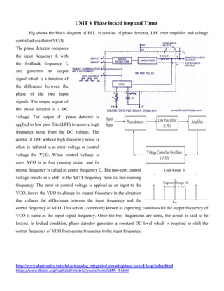
  • 1. UNIT V Phase locked loop and Timer Fig shows the block diagram of PLL. It consists of phase detector, LPF error amplifier and voltage controlled oscillator(VCO). The phase detector compares the input frequency fs with the feedback frequency fo and generates an output signal which is a function of the difference between the phase of the two input signals. The output signal of the phase detector is a DC voltage. The output of phase detector is applied to low pass filter(LPF) to remove high frequency noise from the DC voltage. The output of LPF without high frequency noise is often is referred to as error voltage or control voltage for VCO. When control voltage is zero, VCO is in free running mode and its output frequency is called as center frequency fo. The non-zero control voltage results in a shift in the VCO frequency from its free running frequency. The error or control voltage is applied as an input to the VCO, forces the VCO to change its output frequency in the direction that reduces the differences between the input frequency and the output frequency of VCO. This action , commonly known as capturing, continues till the output frequency of VCO is same as the input signal frequency. Once the two frequencies are same, the circuit is said to be locked. In locked condition, phase detector generates a constant DC level which is required to shift the output frequency of VCO from centre frequency to the input frequency. http://www.electronics-tutorial.net/analog-integrated-circuits/phase-locked-loop/index.html https://www.ibiblio.org/kuphaldt/electricCircuits/Semi/SEMI_4.html
  • 2. IMPORTANT PARAMETER Lock Range When PLL is in lock, it can track frequency changes in the incoming signal. The range of frequencies over which the PLL can maintain lock with the incoming signal is called the lock range or tracking range of the PLL. It is usually expressed as a percentage of fo the VCO frequency. Capture range The range of frequency changes in the incoming signal. The range of frequency over which the PLL can maintain lock with the incoming signal is called the capture range. It is also expressed as a percentage of fo Phase Detector/Comparator: Phase detector is an important part of PLL system. There are two types of phase detectors are used, analog and digital. Analog phase detector The principle of analog phase detection using switch type phase detector is shown above. An electronic switch is opened and closed by signal coming from VCO (normally a square wave ) as shown in figure . The input signal is therefore chopped at a repetition rate determined by VCO frequency. The following figure shows the input signal Vs assumed to be in phase (ɸ=0̊) with VCO output. The analog phase detector is basically a simple electronic switch as shown in figure below, Since the switch is closed only when VCO output is positive, the output waveform (error voltage) Ve will be half sinusoids. Similarly, the output waveforms for ɸ = 90̊ and ɸ = 180̊ is shown in figure. This type of phase detector is called a half wave detector, since the phase information for only one-half of the input waveform is detected and averaged. The output of the phase comparator when filtered through a low pass filter gives an error signal which is the average value of the output waveform shown by dotted line in figure . It
  • 3. may be seen that the error voltage is zero when the phase shift between the two inputs is 90̊. So to achieve a perfect locked condition, the VCO output should be 90̊ out of phase with respect to the input signal. Digital phase detector: The following figure shows the digital type Ex-OR (Exclusive OR) phase detector. The output of the EX-OR gate is HIGH only when one of the input signals is high. it can be seen that the maximum dc output voltage occurs when the phase difference is π (180̊) because output of the gate remains high throughout. The slope of the curve gives the conversation ratio kɸ of the phase detector. EX-OR phase detector can be realized using ICs such as CD 4070. The output dc voltage depends on the duty cycle of the input waveforms. Therefore, this type of phase detector is employed when the waveforms of input signal and output signal are square waves with 50% duty cycle. Voltage Controlled Oscillator IC 566 The figure below shows the block diagram of LM566 IC in which current sources charge and discharge the external capacitor at its rate set by the resistor R1 and also controls the DC input voltage. For switching the capacitor between charging and discharging, a Schmitt trigger circuit is used as shown in figure. The square wave voltage developed from Schmitt trigger and the triangular voltage across capacitor are provided as outputs through buffer amplifiers. Referring to the circuit in the above figure, the capacitor CT is linearly charged or discharged by a constant current source/sink. The amount of current can be controlled by changing the voltage Vc applied at the modulating input (pin 5) or by changing the timing resistor RT external to the IC chip. The voltage at pin 6 is held at the same voltage as pin 5. Thus, if the modulating voltage at pin 5 is increased, the voltage at pin 6 also increases, resulting in less voltage across R1 and thereby decreasing the charging current. The voltage
  • 4. across the capacitor CT is applied to the inverting input terminal of Schmitt trigger via buffer amplifier. The output voltage swing of the Schmitt trigger is designed to Vcc and 0.5 Vcc. If Ra = Rb in the positive feedback loop, the voltage at the non-inverting input terminal of Schmitt trigger swings from 0.5 Vcc to 0.25 Vcc. When the voltage on the capacitor c1 exceeds 0.5 Vcc during charging, the output of the Schmitt trigger goes LOW (0.5 Vcc). The capacitor now discharges and when it is at 0.25 Vcc, the output of Schmitt trigger goes HIGH (Vcc). Since the source and sink currents are equal, capacitor charges and discharges for the same amount of time. This gives a triangular voltage waveform across c1 which is also available at pin 4. The square wave output of the Schmitt trigger is inverted by buffer amplifier at pin 3. The output waveforms are shown near the pins 4 and 3 APPLICATIONS OF PLL  Frequency multiplication, Frequency synthesizer, Frequency translation, AM detection  FM detection Frequency multiplication Fig shows block diagram for a frequency multiplier using PLL 565. Here, a divide by N network is inserted between the VCO output (pin 4) and the phase comparator input (pin 5). Since the output of the divider is locked to the input frequency fi the VCO is actually running at a multiple of the input frequency. Therefore, in the locked state, the VCO output frequency fo is given by, fo=Nfi  By selecting proper divider by N network we can obtain desired multiplication. Frequency translation In some applications we want to shift the input frequency (fin) by a small amount and not by multiple numbers. This shift is called as frequency translation (fT). It is useful in communication systems. While transmission, a carrier frequency is used which is highly stable. A stable frequency generated by crystal is called reference frequency and numbers of other frequencies are generated from PLL. Since the PLL IC is available in low cost, the system is not costly. The following figure shows the block diagram of frequency translator.
  • 5. Externally multiplier (or mixer) and LPF are added. Multiplier is basically a non-linear circuit. Input for multipliers are fref and VCO frequency fo. Let fref is 1 MHz and we want to shift it to a value 1.2 MHz So there is a frequency translation of 0.2 MHz. At the output of multiplier, we have number of frequency components including addition and difference frequencies i.e. (fo ± fref). This frequency is passed through LPF. The output of LPF is the difference signal i.e. (fo-fref). The external frequency (translation frequency) is selected such that it is equal to translation required. In the above example fT = 0.2 MHz. Thus to achieve the locked condition, the two input frequencies for phase detector must be equal. ∴fo-fref=fT; ∴fo=fT+fref ; ∴fo=fT+fref; ∴fo=(0.2+1)MHz; ∴fo=1.2 MHz Thus the reference frequency is shifted from 1 MHz to 1.2 MHz and when the locked condition is achieved, this output frequency is highly stable i.e. translated frequency is also stable. Thus by using PLL, from a single reference frequency we can generate number of stable frequencies by this method of translation. AM Demodulation PLL may be used to demodulate AM signals as shown in the figure below. The PLL is locked to the carrier frequency of the incoming AM signal. The output of VCO which has the same frequency as the carrier, but un-modulated is fed to the multiplier. Since VCO output is always 900 before being fed to the multiplier. This makes both the signals applied to the multiplier and the difference signals, the demodulated output is obtained after filtering high frequency components by the LPF. Since the PLL responds only to the carrier frequencies which are very close to the VCO output, a PLL AM detector exhibits high degree of selectivity and noise immunity which is not possible with conventional peak detector type AM modulators. FM Demdulation The working of a PLL FM demodulator is very easy to understand. The input FM signal and the output of the VCO is applied to the phase detector circuit. The output of the phase detector is filtered using a low pass filter, the amplifier and then used for controlling the VCO. When there is no carrier modulation and the input FM signal is in the center of the pass band (i.e. carrier wave only) the VCO’s tune line voltage will be at the center position. When deviation in carrier frequency occurs ( that means modulation occurs) the VCO frequency follows the
  • 6. input signal in order to keep the loop in lock. As a result the tune line voltage to the VCO varies and this variation is proportional to the modulation done to the FM carrier wave. This voltage variation is filtered and amplified in order to get the demodulated signal. 555 Timer Block Diagram of 555 timer Construction The block diagram of a 555 timer is shown in the above figure. A 555 timer has two comparators, which are basically 2 op-amps), an R-S flip-flop, two transistors and a resistive network. 1. Resistive network consists of three equal resistors and acts as a voltage divider. 2. Comparator 1 compares threshold voltage with a reference voltage + 2/3 VCCvolts. 3. Comparator 2 compares the trigger voltage with a reference voltage + 1/3 VCCvolts. Output of both the comparators is supplied to the flip-flop. Flip-flop assumes its state according to the output of the two comparators. One of the two transistors is a discharge transistor of which collector is connected to pin 7. This transistor saturates or cuts-off according to the output state of the flip-flop. The saturated transistor provides a discharge path to a capacitor connected externally. Base of another transistor is connected to a reset terminal. A pulse applied to this terminal resets the whole timer irrespective of any input. Working Principle The internal resistors act as a voltage divider network, providing (2/3)Vcc at the non-inverting terminal of the upper comparator and (1/3)Vcc at the inverting terminal of the lower comparator. In most applications, the control input is not used, so that the control voltage equals +(2/3) VCC. Upper comparator has a threshold input (pin 6) and a control input (pin 5). Output of the upper comparator is applied to set (S)
  • 7. input of the flip-flop. Whenever the threshold voltage exceeds the control voltage, the upper comparator will set the flip-flop and its output is high. A high output from the flip-flop when given to the base of the discharge transistor saturates it and thus discharges the transistor that is connected externally to the discharge pin 7. The complementary signal out of the flip-flop goes to pin 3, the output, available at pin 3 is low. These conditions will prevail until lower comparator triggers the flip-flop. Even if the voltage at the threshold input falls below (2/3) VCC, that is upper comparator cannot cause the flip-flop to change again. It means that the upper comparator can only force the flip-flop’s output high. To change the output of flip-flop to low, the voltage at the trigger input must fall below + (1/3) Vcc. When this occurs, lower comparator triggers the flip-flop, forcing its output low. The low output from the flip-flop turns the discharge transistor off and forces the power amplifier to output a high. These conditions will continue independent of the voltage on the trigger input. Lower comparator can only cause the flip-flop to output low. From the above discussion it is concluded that for the having low output from the timer 555, the voltage on the threshold input must exceed the control voltage or + (2/3) VCC. This also turns the discharge transistor on. To force the output from the timer high, the voltage on the trigger input must drop below +(1/3) VCC. This turns the discharge transistor off. The important features of the 555 timer are : 1. It operates from a wide range of power supplies ranging from + 5 Volts to + 18 Volts supply voltage. 2. Sinking or sourcing 200 mA of load current. 3. The external components should be selected properly so that the timing intervals can be made into several minutes along with the frequencies exceeding several hundred kilo hertz. 4. The output of a 555 timer can drive a transistor-transistor logic (TTL) due to its high current output. 5. It has a temperature stability of 50 parts per million (ppm) per degree Celsius change in temperature, or equivalently 0.005 %/ °C. 6. The duty cycle of the timer is adjustable. 7. The maximum power dissipation per package is 600 mW and its trigger and reset inputs has logic compatibility. More features are listed in the datasheet. Application of 555 timer Astable multivibrator
  • 8. In the 555 Oscillator circuit above, pin 2 and pin 6 are connected together allowing the circuit to re-trigger itself on each and every cycle allowing it to operate as a free running oscillator. During each cycle capacitor, C1 charges up through both timing resistors, R1and R2 but discharges itself only through resistor, R2 as the other side of R2 is connected to the discharge terminal, pin 7. Then the capacitor charges up to 2/3Vcc (the upper comparator limit) which is determined by the 0.693(R1+R2)C1 combination and discharges itself down to 1/3Vcc (the lower comparator limit) determined by the 0.693(R2.C1) combination. This results in an output waveform whose voltage level is approximately equal to Vcc – 1.5V and whose output “ON” and “OFF” time periods are determined by the capacitor and resistors combinations. The individual times required to complete one charge and discharge cycle of the output is therefore given as: The capacitor voltage for a low pass circuit to a step input of VCC volts is VC=VCC(1-e-t/RC ) t1 by the circuit to change from 0 to (2/3) VCC is (2/3) VCC = 1 / (1 )t RC ccV e  ;t1 =1.09 RC t2 by the circuit to change from 0 to (1/3) VCC is (1/3) VCC = / (1 )t RC ccV e  ;t2 =0.405 RC so the time to charge from (1/3) VCC to (2/3) VCC is tHIGH = t1- t2; tHIGH=1.09 RC-0.405 RC so for the given circuit tHIGH=0.69(C)C the output is low while the capacitor discharges from (2/3) VCC to (1/3) VCC and the voltage across the capacitor is given by (1/3) VCC =(2/3) VCC / (1 )t RC e  solving, we get t= 0.69RC So, for the given circuit, tlow=0.69RBC Notice that both R1 and R2 are in the charge path, but only R2 is the discharge path. Therefore total time, T= tHIGH+ tlow T=0.69(R1+ 2R2) C; f= 1/T=1/((R1+ 2R2) C Mono-stable operation
  • 9. Working of Monostable Multivibrator with 555 Timer Circuit 1. The output of the monostable multivibrator using 555 timer remains in its stable state until it gets a trigger. 2. In monostable 555 multivibrator, when both the transistor and capacitor are shorted then this state is called as a stable state. 3. When the voltage goes below at the second pin of the 555 IC, the o/p becomes high. This high state is called quasi stable state. When the circuit activates then the transition from a stable state to quasi stable state. 4. Then the discharge transistor is cut off and capacitor starts charging to VCC. Charging of the capacitor is done via the resistor R1 with a time constant R1C1 5. Hence, the voltage of the capacitor increases and finally exceeds 2/3 Vcc, it will change the internal control flip flop, thereby turning off the 555 timer IC 6. Thus the o/p goes back to its stable state from an unstable state. We know that the voltage across the capacitor C rises exponentially. Hence the equation for the capacitor voltage VC can be written as VC = VCC (1 – e-t/RC ) When the capacitor voltage is 2/3 VCC, then 2/3 VCC = VCC (1 – e-t/RC ) 2/3 = 1 – e-t/RC e-t/RC = 1/3 – t/RC = ln (1/3) – t/RC = -1.098 t = 1.098 RC Schmitt trigger The two comparator inputs (pin 2 & 6) are tied together and biased at 1/2 Vcc through a voltage divider R1 and R2.Since the threshold comparator will trip at 2/3 Vcc and the trigger comparator will trip at 1/3Vcc,the bias provided by the resistors R1 & R2 are centered within the comparators trip limits. The important characteristic of the Schmitt trigger is Hysteresis. The output of the Schmitt trigger is high if the input voltage is greater than the upper threshold value and the output of the Schmitt trigger is low if the input voltage is lower than the lower threshold value.
  • 10. The threshold values in this case are 2/3 VCC and 1/3 VCC i.e. the upper comparator trips at 2/3 VCC and the lower comparator trips at 1/3 VCC. The input voltage is compared to these threshold values by the individual comparators and the flip-flop is SET or RESET accordingly. Based on this the output becomes high or low. When a sine wave of amplitude greater than VCC / 6 is applied at the input, the flip-flop is set and reset alternately for the positive cycle and the negative cycle. The output is a square wave and the waveforms for input sine wave and output square wave are shown below. Missing pulse detector The train of trigger pulses will continuously reset the timing cycle. Hence the output is always high. If any trigger pulse is missing, the device detects this missing pulse and the output goes low. The detailed working is as follows. When the input is 0, the PNP transistor is turned ON and the voltage across the capacitor is clamped to 0.7 V and the output is HIGH. When the input trigger voltage is high, the transistor is cut-off and the capacitor will start charging. If the input trigger signal goes low again before the completion of the timing cycle, the voltage across the capacitor falls to 0.7 V before reaching the threshold voltage (2/3 VCC) and the output continues to remain HIGH. If the input trigger signal doesn’t go low before the completion of the timing cycle due to a missing pulse, it allows the capacitor to charge to the threshold voltage and the output will become LOW. In order to make this circuit work as a Missing Pulse Detector, the time period of the input trigger signal should be slightly lesser than the timing interval. Because of this, the continuous negative going input pulses will not allow the capacitor to charge till the threshold voltage. And the output continues to stay high. In case of change of input frequency or a missing pulse, the capacitor will charge to the threshold voltage and the output falls low. The waveforms of the input pulse, voltage on the capacitor and the output signal are shown below.
  • 11. Dual timer The 556 timer is a dual version of the 555 timer. In other words it is embedded with two 555 timers operating separately. The CMOS versions offer improved characteristics for particular applications. The two timers operate independently of each other sharing only Vs and ground. The circuit may be triggered and reset on falling waveforms. The 556 timer is a 14 pin configuration is shown in figure. Each Timer is provided with its own threshold, trigger, discharge, control, reset and output pins. This IC can be used for both the oscillator as well as pulse generator due to availability of two separate 555 timers. Usually a 555 timer is used as an oscillator in astable mode, whereas it is used as a pulse generator in monostable mode. 556 Applications  Precision timing  Pulse generation  Sequential timing  Time delay generation  Pulse width modulation  Pulse position modulation