An analysis of pfc converter with high speed dynamic
research_report (1)
1. Simulation of Charge Pump PLL based frequency
synthesizer using simulink
Diksha Sharma, Akhil Mittal
Department of Electronics & communication
Chitkara University, Solan, India
diksha001995@gmail.com, akhilmittal510@gmail.com
Abstract— A novel structure of a charge pump phase-locked loop
(PLL) based frequency synthesizer characterized by a low settling
time and fast locking is presented. Simulation of a frequency
synthesizer has been illustrated in this paper. The synthesizer
generates a signal of 500Mhz with the input frequency of 25Mhz. All
the PLL building blocks are modeled and simulated using Simulink.
The PLL performance has been evaluated using MATLAB. The
performance parameters are compared with other standard and
latest charge pump based architectures of PLL. The PLL
implemented using proposed charge pump is found to exhibit very
low locking time of 0.80uS(approximately) with ideal stability. In
addition, the effect of the VCO gain, loop filter order and loop
bandwidth on the reference spurs level are taken into consideration.
Keywords—phase locked loop; frequency synthesizer; simulink;
charge pump;
I. INTRODUCTION
Nowadays, high performance frequency synthesizers
are often required to fast lock-in time and low jitter.
Meanwhile, fast frequency switching of frequency
synthesizers is one of the challenges in modern wireless
communications. How fast the communication channels can
be switched and how fast the system can be turned on/off
depend on the lock-in time. In this paper, a fast-settling
frequency synthesizer with fast start-up and slope charge
pump current control is presented, on the basis of which, a
better stability, a shorter locking time and lower jitter are
obtained. The PLL performance depends upon its order. If n is
the order of loop filter than n+1 is the order of PLL. The
stability of the whole PLL system depends on the order of the
loop filter. The comparison of the performances of the other
designs are presented, which shows the improved
characteristics of our design.
A PLL is a feedback system that compares the phases of two
inputs and generates equivalent output according to the
difference obtained. The PLL module consists of a Voltage-
Controlled Oscillator (VCO), frequency divider,
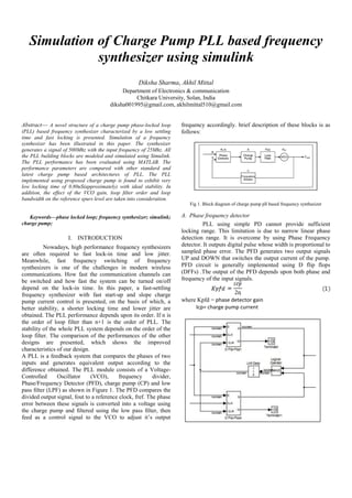
Phase/Frequency Detector (PFD), charge pump (CP) and low
pass filter (LPF) as shown in Figure 1. The PFD compares the
divided output signal, fout to a reference clock, fref. The phase
error between these signals is converted into a voltage using
the charge pump and filtered using the low pass filter, then
feed as a control signal to the VCO to adjust it’s output
frequency accordingly. brief description of these blocks is as
follows:
II. EASE OF USE
Fig 1. Block diagram of charge pump pll based frequency synthesizer
A. Phase frequency detector
PLL using simple PD cannot provide sufficient
locking range. This limitation is due to narrow linear phase
detection range. It is overcome by using Phase Frequency
detector. It outputs digital pulse whose width is proportional to
sampled phase error. The PFD generates two output signals
UP and DOWN that switches the output current of the pump.
PFD circuit is generally implemented using D flip flops
(DFFs) .The output of the PFD depends upon both phase and
frequency of the input signals.
where Kpfd = phase detector gain
Icp= charge pump current
2. Fig 2: Simulink design of phase frequency detector
B. Charge pump filter
It converts digital error pulse to analog error current and
integrates (and low-pass filters in continuous time) the error
current to generate VCO control voltage. The output voltage
of the loop filter controls the oscillation frequency of the
VCO. The loop filter voltage will increase if fref leads fin and
will decrease if Fin leads fref. If the PLL is in locked state it
maintains a constant value.
A series combination of resistor R1 and capacitor C1 is giving
zeros and poles to the transfer function of filter respectively.
An extra capacitor C2 is added to avoid ringing and reference
spur. It is adding an extra pole in the transfer function by
lowering the phase margin. Generally its value is taken as
C2=(C1/10).
Fig 3. simulink design of charge pump filter
II. DAMPING RATIO, NATURAL FREQUENCY,
BANDWIDTH
where N= divider ratio
C1= capictance of first capacitor
C2= capacitance of second capacitor
Ѡn= natural frequency
where ξ= damping factor
then we can get the loop bandwidth Ѡc:
open loop transfer function
Now consider a PLL which is initially locked at frequency 0,
and then the system is changed to cause the PLL to switch to
frequency fout. This is equivalent to changing the reference
frequency from 0 to fout/N. Using inverse Laplace transforms,
the time frequency response is obtained, from which the lock
time of the PLL is derived as
where t is the locking time and k corresponds to the maximum
tolerance of the frequency at which the PLL is considered to
be locked. So, the lock time is inversely proportional to the
loop bandwidth Ѡc, which is proportional to Ip. In other
words, to modulate the lock time we can modulate the charge
pump current and so the loop bandwidth.
III. STABILITY
Stability of design is found out by designing bode plot,
root-locus diagram of transfer function of third order PLL.
The obtained bode plot and root locus is shown in figure.
Phase margin of system is 56.56 degree.
Fig 4. Bode diagram
Fig 5. Root locus plot
IV. DESIGN CONSTRAINTS
Bandwidth needs to ne 1/10 of reference frequency
for system stability purpose. with very small
3. bandwidth PLL begins to lose the lock very soon
with reference
if ξ is less, step response exhibits high amplitude
oscillations before settling so appropriate value
should be chosen.(ξ~1)
With high vco sensitivity, small jump in control
voltage results a large jump in output frequency
Resistor in LPF provides an instantaneous IR on the
control voltage causing the VCO V2I to generate a
current bump on the oscillator output. so a small
value of R and high value of C should be chosen so
that damping can be decreased
V. EXPERIMENTAL RESULT ANALYSIS
The simulation is done in Simulink/Matlab 2009b .The
simulated results for filter output ,phase detector output and
VCO outputs can seen in real time using scope in Simulink.
The obtained VCO output filter output, Final output for
Charge pump PLL is shown in figure 6, figure 7 resepectively.
Fig 6. Charge pump filter output
Fig 7. PLL output
Fig 8. Step response of charge pump PLL
Figure 8 shows the step response of third order system in
which settling time comes out to be 3.2uS. Figure 4 shows the
loop stability under the slope charge pump current depending
on the design of Eqs. (2)–(6). From Fig. 4 we can see that the
loop bandwidth can be adjusted by the slope charge pump
current with good stability. The phase margin is well
controlled in the stable range under the different output
frequencies and slope charge pump current. Therefore, the
locking time is optimized with the slope charge pump current.
TABLE I. RESULT ANALYSIS
PARAMETER RESULT
Input voltage(v) 1
Output voltage(v) 0.9
Operating frequency(Mhz) 25
Output frequency (Mhz) 500
Pull-in and pull down current(uA) 172
Loop bandwidth(Mhz) 2.5
Phase margin(degree) 56.1205
Vco sensitivity (Mhz/V) 500
Locking time(uS) 0.8
Settling time 3.2
VI. CONCLUSION
In this paper, a charge pump PLL based frequency
synthesizer application has been designed and simulated using
the simulink. The simple and symmetric structure of the
circuit reduces spurious jitter phenomenon and provide more
stable operation under a 1 V power supply without use of op-
amp circuit. It has output voltage of 0.9V and more stable step
voltage. The pull-up current I1 and the pull down current I2
are both set to 172μA. The operating frequency is 25MHz and
gives output frequency of 500Mhz.
References
[1] Razavi, B., K.F. Lee and R.H. Yan, 1995. ―Design of high-speed, low-
power frequency dividers and phase-locked loops in deep submicron
CMOS,‖ IEEE J. Solid-State Circuits, 30: 101-109. J. Clerk Maxwell, A
Treatise on Electricity and Magnetism, 3rd ed., vol. 2. Oxford:
Clarendon, 1892, pp.68-73.
[2] Razavi B., 2005. Design of Analog CMOS Integrated Circuits [M].
Beijing: Tsinghua University Press,K. Elissa, ―Title of paper if known,‖
unpublished.
[3] W.-Y. Choi. Charge-Pump PLL, Electronic Circuits 2 (09/1),lect-24
[4] Guo Zhongjie,Liu Youbao, Wu Longsheng, Wang Xihu, and Tang
Wei,2010.‖ Short locking time and low jitter phase-locked loop based on
slope charge pump control ‖ Journal of Semiconductor: Vol. 31, No. 10
[5] Yogendra Pratap Singh,Dr. R.K. Chauhan.‖Fast Charge Pump Circuit
for PLL using 50nm CMOS Technology‖ International Journal of
Advanced Research in Computer and Communication Engineering Vol.
2,Issue7,July2013
[6] Hung, C.H. and K.O. Kenneth, 2002. "A fully integrated 1.5-V 5.5-GHz
CMOS phase locked loop". IEEEJournal of Solid-State Circuits 37: 521-
525.