SlideShare a Scribd company logo
1 of 2
           The gap between the top of the valence band and bottom of the conduction band is called the energy band gap (Energy gap Eg). It may be large, small, or zero, depending upon the material.<br />Case I: One can have a metal either when the conduction band is partially filled and the balanced band is partially empty or when the conduction and valance bands overlap. When there is overlap electrons from valence band can easily move into the conduction band. This situation makes a large number of electrons available for electrical conduction. When the valence band is partially empty, electrons from its lower level can move to higher level making conduction possible. Therefore, the resistance of such materials is low or the conductivity is high.<br />      CB<br />          CB<br />VB          VB                                                                                                                  Overlap<br /> <br />Case II:  In this case, as shown in Fig. A large band gap Eg exists (Eg > 3 eV). There are no electrons in the conduction band, and therefore no electrical conduction is possible. Note that the energy gap is so large that electrons cannot be excited from the valence band to the conduction band by thermal excitation. This is the case of insulators.<br /> <br /> CB<br /> <br /> Eg(>3 eV)<br /> <br />          VB<br />Case III: This situation is shown in Fig.  Here a finite but small band gap (Eg < 3 eV) exists. Because of the small band gap, at room temperature some electrons from valence band can acquire enough energy to cross the energy gap and enter the conduction band. These electrons (though small in numbers) can move in the conduction band. Hence, the resistance of semiconductors is not as high as that of the insulators.<br /> CB<br />  Eg(<3 eV)<br /> VB<br />Semiconductors<br />Based on the purity, semiconductors are classified into two types,<br />1. Intrinsic semiconductor and<br />2. Extrinsic semiconductor.<br />Intrinsic semiconductor<br />A semiconductor which is pure and contains no impurity is known as an intrinsic semiconductor. Example: pure germanium (Ge) and silicon (Si).<br /> Each Si and Ge atom is surrounded by four nearest neighbours. We know that Si and Ge have four valence electrons. In its crystalline structure, every Si or Ge atom tends to share one of its four valence electrons with each of its four nearest neighbour atoms, and also to take share of one electron from each such neighbour. These shared electrons pairs are referred to as forming a covalent bond.<br />Fig. Intrinsic semiconductor<br />As the temperature increases, more thermal energy becomes available to these electrons and some of these electrons may break–away (becoming free electrons contributing to conduction). The thermal energy effectively ionizes only a few atoms in the crystalline lattice and creates a vacancy in the bond.  <br />The neighbourhood, from which the free electron (with charge –q) has come out leaves a vacancy with an effective charge (+q). This vacancy with the effective positive electronic charge is called a hole. The hole behaves as an apparent free particle with effective positive charge.<br />An intrinsic semiconductor will behave like an insulator at T = 0 K as shown in Fig. It is the thermal energy at higher temperatures (T > 0K), which excites some electrons from the valence band to the conduction band. These thermally excited electrons at T > 0 K, partially occupy the conduction band. Therefore, the energy-band diagram of an intrinsic semiconductor will be as shown in Fig. Here, some electrons are shown in the conduction band. These have come from the valence band leaving equal number of holes there.<br />In intrinsic semiconductors, the number of free electrons, ne is equal to the number of holes, nh. That is ne = nh = ni<br />Where ni is called intrinsic carrier concentration.<br />
Semi conductors

More Related Content

What's hot

semiconductor physics,unit 5
semiconductor physics,unit 5semiconductor physics,unit 5
semiconductor physics,unit 5Kumar
 
Energy band and energy gap by Pratimesh pathak
Energy band and energy gap by Pratimesh pathakEnergy band and energy gap by Pratimesh pathak
Energy band and energy gap by Pratimesh pathakPratimesh Pathak
 
SEMICONDUCTOR (project)
SEMICONDUCTOR (project)SEMICONDUCTOR (project)
SEMICONDUCTOR (project)SUDHA BHUJEL
 
Led presentation
Led presentationLed presentation
Led presentationAB Amit
 
Semiconductor.pdf description ki last lin...
Semiconductor.pdf                                     description ki last lin...Semiconductor.pdf                                     description ki last lin...
Semiconductor.pdf description ki last lin...KALPESH-JNV
 
semiconductor physics
semiconductor physics semiconductor physics
semiconductor physics ruwaghmare
 
CBSE Class XII Physics Investigatory Project
CBSE Class XII Physics Investigatory ProjectCBSE Class XII Physics Investigatory Project
CBSE Class XII Physics Investigatory ProjectVaibhav Kandwal
 
A BASIC INTRODUCTION TO SEMICONDUCTOR DEVICES - THE
A BASIC INTRODUCTION TO SEMICONDUCTOR DEVICES - THEA BASIC INTRODUCTION TO SEMICONDUCTOR DEVICES - THE
A BASIC INTRODUCTION TO SEMICONDUCTOR DEVICES - THEWinston Bent A.S.S.
 
Electrostatics Class 12- Part 4
Electrostatics Class 12- Part 4Electrostatics Class 12- Part 4
Electrostatics Class 12- Part 4Self-employed
 
Semiconductor Devices Class 12 Part-2
Semiconductor Devices Class 12 Part-2Semiconductor Devices Class 12 Part-2
Semiconductor Devices Class 12 Part-2Self-employed
 
Introduction to semiconductor materials
Introduction to semiconductor materialsIntroduction to semiconductor materials
Introduction to semiconductor materialsDr. Ghanshyam Singh
 
Physics Investigatory:To Study V-I Characteristics Of Zener Diode
Physics Investigatory:To Study V-I Characteristics Of Zener DiodePhysics Investigatory:To Study V-I Characteristics Of Zener Diode
Physics Investigatory:To Study V-I Characteristics Of Zener DiodeGautammaini9
 
Nuclei And Atoms Class 12
Nuclei And Atoms Class 12Nuclei And Atoms Class 12
Nuclei And Atoms Class 12Self-employed
 

What's hot (20)

semiconductor physics,unit 5
semiconductor physics,unit 5semiconductor physics,unit 5
semiconductor physics,unit 5
 
Semiconductor Physics
Semiconductor PhysicsSemiconductor Physics
Semiconductor Physics
 
Unit 2 semiconductors
Unit 2  semiconductors Unit 2  semiconductors
Unit 2 semiconductors
 
'12th semiconductors'
'12th semiconductors''12th semiconductors'
'12th semiconductors'
 
Energy band and energy gap by Pratimesh pathak
Energy band and energy gap by Pratimesh pathakEnergy band and energy gap by Pratimesh pathak
Energy band and energy gap by Pratimesh pathak
 
Half wave rectifier
Half wave rectifierHalf wave rectifier
Half wave rectifier
 
SEMICONDUCTOR (project)
SEMICONDUCTOR (project)SEMICONDUCTOR (project)
SEMICONDUCTOR (project)
 
Led presentation
Led presentationLed presentation
Led presentation
 
Semiconductor.pdf description ki last lin...
Semiconductor.pdf                                     description ki last lin...Semiconductor.pdf                                     description ki last lin...
Semiconductor.pdf description ki last lin...
 
Semiconductor diode
Semiconductor diodeSemiconductor diode
Semiconductor diode
 
semiconductor physics
semiconductor physics semiconductor physics
semiconductor physics
 
CBSE Class XII Physics Investigatory Project
CBSE Class XII Physics Investigatory ProjectCBSE Class XII Physics Investigatory Project
CBSE Class XII Physics Investigatory Project
 
A BASIC INTRODUCTION TO SEMICONDUCTOR DEVICES - THE
A BASIC INTRODUCTION TO SEMICONDUCTOR DEVICES - THEA BASIC INTRODUCTION TO SEMICONDUCTOR DEVICES - THE
A BASIC INTRODUCTION TO SEMICONDUCTOR DEVICES - THE
 
Electrostatics Class 12- Part 4
Electrostatics Class 12- Part 4Electrostatics Class 12- Part 4
Electrostatics Class 12- Part 4
 
Semiconductor Devices Class 12 Part-2
Semiconductor Devices Class 12 Part-2Semiconductor Devices Class 12 Part-2
Semiconductor Devices Class 12 Part-2
 
Introduction to semiconductor materials
Introduction to semiconductor materialsIntroduction to semiconductor materials
Introduction to semiconductor materials
 
Physics Investigatory:To Study V-I Characteristics Of Zener Diode
Physics Investigatory:To Study V-I Characteristics Of Zener DiodePhysics Investigatory:To Study V-I Characteristics Of Zener Diode
Physics Investigatory:To Study V-I Characteristics Of Zener Diode
 
Semiconductors
SemiconductorsSemiconductors
Semiconductors
 
EC 8353 EDC
EC 8353 EDCEC 8353 EDC
EC 8353 EDC
 
Nuclei And Atoms Class 12
Nuclei And Atoms Class 12Nuclei And Atoms Class 12
Nuclei And Atoms Class 12
 

Viewers also liked (20)

Analysis of ship management for better practices
Analysis of ship management for better practicesAnalysis of ship management for better practices
Analysis of ship management for better practices
 
Semi conductors
Semi conductorsSemi conductors
Semi conductors
 
Shipmanagement System Selection Process
Shipmanagement System Selection ProcessShipmanagement System Selection Process
Shipmanagement System Selection Process
 
Ss for b,ed
Ss for b,edSs for b,ed
Ss for b,ed
 
ISPS REVIVE
ISPS REVIVEISPS REVIVE
ISPS REVIVE
 
17th Edition Part 4 3
17th  Edition  Part 4 317th  Edition  Part 4 3
17th Edition Part 4 3
 
pn junction diodes
pn junction diodespn junction diodes
pn junction diodes
 
Transistor
TransistorTransistor
Transistor
 
Ship dry docking
Ship dry dockingShip dry docking
Ship dry docking
 
Auxiliary machinery
Auxiliary machineryAuxiliary machinery
Auxiliary machinery
 
Ship Organization
Ship OrganizationShip Organization
Ship Organization
 
ISM Code
ISM CodeISM Code
ISM Code
 
Light-emitting diodes
Light-emitting diodes Light-emitting diodes
Light-emitting diodes
 
Ship survey presentation
Ship survey presentationShip survey presentation
Ship survey presentation
 
2 classification societies
2 classification societies2 classification societies
2 classification societies
 
Pipe Fittings and Valves for Marine Use
Pipe Fittings and Valves for Marine UsePipe Fittings and Valves for Marine Use
Pipe Fittings and Valves for Marine Use
 
Zener diodes
Zener diodesZener diodes
Zener diodes
 
Parts of a Ship Engine
Parts of a Ship Engine Parts of a Ship Engine
Parts of a Ship Engine
 
Edc(electronics devices and circuits)
Edc(electronics devices and circuits)Edc(electronics devices and circuits)
Edc(electronics devices and circuits)
 
Diodes
DiodesDiodes
Diodes
 

Similar to Semi conductors

ENERGY BANDS AND EFFECTIVE MASSppt
ENERGY BANDS AND EFFECTIVE MASSpptENERGY BANDS AND EFFECTIVE MASSppt
ENERGY BANDS AND EFFECTIVE MASSpptBiswajeetMishra21
 
Semiconductors (rawat d agreatt)
Semiconductors (rawat d agreatt)Semiconductors (rawat d agreatt)
Semiconductors (rawat d agreatt)Rawat DA Greatt
 
semiconductor and hall effect.pptx chemistry .....
semiconductor and hall effect.pptx chemistry .....semiconductor and hall effect.pptx chemistry .....
semiconductor and hall effect.pptx chemistry .....amruthatk3
 
Diploma sem 2 applied science physics-unit 3-chap-1 band theory of solid
Diploma sem 2 applied science physics-unit 3-chap-1 band theory of solidDiploma sem 2 applied science physics-unit 3-chap-1 band theory of solid
Diploma sem 2 applied science physics-unit 3-chap-1 band theory of solidRai University
 
semiconductor-physics-3.pdf. Semiconductor
semiconductor-physics-3.pdf.  Semiconductorsemiconductor-physics-3.pdf.  Semiconductor
semiconductor-physics-3.pdf. SemiconductorMinaNath2
 
TRM-11fhsdbjbfffffffffffffffffffffffffffffffffffffff.ppt
TRM-11fhsdbjbfffffffffffffffffffffffffffffffffffffff.pptTRM-11fhsdbjbfffffffffffffffffffffffffffffffffffffff.ppt
TRM-11fhsdbjbfffffffffffffffffffffffffffffffffffffff.pptsauravnair2003
 
semo conductor.ppt
semo conductor.pptsemo conductor.ppt
semo conductor.pptkasthuri73
 
Topic energy band gap material science ppt
Topic  energy band gap material science pptTopic  energy band gap material science ppt
Topic energy band gap material science pptSubhashYadav144
 
Unit1.2 Band Theory of Solids
Unit1.2 Band Theory of SolidsUnit1.2 Band Theory of Solids
Unit1.2 Band Theory of SolidsFarhat Ansari
 
Module 1 Semiconductors (1).pptx
Module 1  Semiconductors (1).pptxModule 1  Semiconductors (1).pptx
Module 1 Semiconductors (1).pptxPriyaSharma135745
 
UNIT 3 Analog Electronics.pptx
UNIT 3 Analog Electronics.pptxUNIT 3 Analog Electronics.pptx
UNIT 3 Analog Electronics.pptxDHARUNESHBOOPATHY
 
B.tech sem i engineering physics u ii chapter 1-band theory of solid
B.tech sem i engineering physics u ii chapter 1-band theory of solidB.tech sem i engineering physics u ii chapter 1-band theory of solid
B.tech sem i engineering physics u ii chapter 1-band theory of solidRai University
 
хагас дамжуулагчийн физик
хагас дамжуулагчийн физикхагас дамжуулагчийн физик
хагас дамжуулагчийн физикJkl L
 
Band theory of solids
Band theory of solidsBand theory of solids
Band theory of solidsutpal sarkar
 
Fisika Modern 15 molecules andsolid_semiconductor
Fisika Modern 15 molecules andsolid_semiconductorFisika Modern 15 molecules andsolid_semiconductor
Fisika Modern 15 molecules andsolid_semiconductorjayamartha
 
Fisika Modern 15 molecules andsolid_semiconductor
Fisika Modern 15 molecules andsolid_semiconductorFisika Modern 15 molecules andsolid_semiconductor
Fisika Modern 15 molecules andsolid_semiconductorjayamartha
 

Similar to Semi conductors (20)

ENERGY BANDS AND EFFECTIVE MASSppt
ENERGY BANDS AND EFFECTIVE MASSpptENERGY BANDS AND EFFECTIVE MASSppt
ENERGY BANDS AND EFFECTIVE MASSppt
 
Semiconductors (rawat d agreatt)
Semiconductors (rawat d agreatt)Semiconductors (rawat d agreatt)
Semiconductors (rawat d agreatt)
 
semiconductor and hall effect.pptx chemistry .....
semiconductor and hall effect.pptx chemistry .....semiconductor and hall effect.pptx chemistry .....
semiconductor and hall effect.pptx chemistry .....
 
Diploma sem 2 applied science physics-unit 3-chap-1 band theory of solid
Diploma sem 2 applied science physics-unit 3-chap-1 band theory of solidDiploma sem 2 applied science physics-unit 3-chap-1 band theory of solid
Diploma sem 2 applied science physics-unit 3-chap-1 band theory of solid
 
semiconductor-physics-3.pdf. Semiconductor
semiconductor-physics-3.pdf.  Semiconductorsemiconductor-physics-3.pdf.  Semiconductor
semiconductor-physics-3.pdf. Semiconductor
 
TRM-11fhsdbjbfffffffffffffffffffffffffffffffffffffff.ppt
TRM-11fhsdbjbfffffffffffffffffffffffffffffffffffffff.pptTRM-11fhsdbjbfffffffffffffffffffffffffffffffffffffff.ppt
TRM-11fhsdbjbfffffffffffffffffffffffffffffffffffffff.ppt
 
semo conductor.ppt
semo conductor.pptsemo conductor.ppt
semo conductor.ppt
 
Topic energy band gap material science ppt
Topic  energy band gap material science pptTopic  energy band gap material science ppt
Topic energy band gap material science ppt
 
Unit1.2 Band Theory of Solids
Unit1.2 Band Theory of SolidsUnit1.2 Band Theory of Solids
Unit1.2 Band Theory of Solids
 
Module 1 Semiconductors (1).pptx
Module 1  Semiconductors (1).pptxModule 1  Semiconductors (1).pptx
Module 1 Semiconductors (1).pptx
 
Chapter 1
Chapter 1Chapter 1
Chapter 1
 
UNIT 3 Analog Electronics.pptx
UNIT 3 Analog Electronics.pptxUNIT 3 Analog Electronics.pptx
UNIT 3 Analog Electronics.pptx
 
B.tech sem i engineering physics u ii chapter 1-band theory of solid
B.tech sem i engineering physics u ii chapter 1-band theory of solidB.tech sem i engineering physics u ii chapter 1-band theory of solid
B.tech sem i engineering physics u ii chapter 1-band theory of solid
 
хагас дамжуулагчийн физик
хагас дамжуулагчийн физикхагас дамжуулагчийн физик
хагас дамжуулагчийн физик
 
Band theory of solids
Band theory of solidsBand theory of solids
Band theory of solids
 
Basic electronics
Basic electronicsBasic electronics
Basic electronics
 
Fisika Modern 15 molecules andsolid_semiconductor
Fisika Modern 15 molecules andsolid_semiconductorFisika Modern 15 molecules andsolid_semiconductor
Fisika Modern 15 molecules andsolid_semiconductor
 
Fisika Modern 15 molecules andsolid_semiconductor
Fisika Modern 15 molecules andsolid_semiconductorFisika Modern 15 molecules andsolid_semiconductor
Fisika Modern 15 molecules andsolid_semiconductor
 
Energy bands and gaps in semiconductor
Energy bands and gaps in semiconductorEnergy bands and gaps in semiconductor
Energy bands and gaps in semiconductor
 
Presentation1.pdf
Presentation1.pdfPresentation1.pdf
Presentation1.pdf
 

More from sunmo

Temple
TempleTemple
Templesunmo
 
Unit II
Unit IIUnit II
Unit IIsunmo
 
Unit i
Unit i Unit i
Unit i sunmo
 
CONDUCTING MATERIALS-BASICS
CONDUCTING MATERIALS-BASICSCONDUCTING MATERIALS-BASICS
CONDUCTING MATERIALS-BASICSsunmo
 
ENGINEERING PHYSICS -SEMICONDUCTING MATERIALS PROBLEMS KEYS
ENGINEERING PHYSICS -SEMICONDUCTING MATERIALS PROBLEMS KEYSENGINEERING PHYSICS -SEMICONDUCTING MATERIALS PROBLEMS KEYS
ENGINEERING PHYSICS -SEMICONDUCTING MATERIALS PROBLEMS KEYSsunmo
 
Electron configuration for all elements
Electron configuration for all elementsElectron configuration for all elements
Electron configuration for all elementssunmo
 

More from sunmo (6)

Temple
TempleTemple
Temple
 
Unit II
Unit IIUnit II
Unit II
 
Unit i
Unit i Unit i
Unit i
 
CONDUCTING MATERIALS-BASICS
CONDUCTING MATERIALS-BASICSCONDUCTING MATERIALS-BASICS
CONDUCTING MATERIALS-BASICS
 
ENGINEERING PHYSICS -SEMICONDUCTING MATERIALS PROBLEMS KEYS
ENGINEERING PHYSICS -SEMICONDUCTING MATERIALS PROBLEMS KEYSENGINEERING PHYSICS -SEMICONDUCTING MATERIALS PROBLEMS KEYS
ENGINEERING PHYSICS -SEMICONDUCTING MATERIALS PROBLEMS KEYS
 
Electron configuration for all elements
Electron configuration for all elementsElectron configuration for all elements
Electron configuration for all elements
 

Recently uploaded

DATA STRUCTURE AND ALGORITHM for beginners
DATA STRUCTURE AND ALGORITHM for beginnersDATA STRUCTURE AND ALGORITHM for beginners
DATA STRUCTURE AND ALGORITHM for beginnersSabitha Banu
 
Hierarchy of management that covers different levels of management
Hierarchy of management that covers different levels of managementHierarchy of management that covers different levels of management
Hierarchy of management that covers different levels of managementmkooblal
 
18-04-UA_REPORT_MEDIALITERAСY_INDEX-DM_23-1-final-eng.pdf
18-04-UA_REPORT_MEDIALITERAСY_INDEX-DM_23-1-final-eng.pdf18-04-UA_REPORT_MEDIALITERAСY_INDEX-DM_23-1-final-eng.pdf
18-04-UA_REPORT_MEDIALITERAСY_INDEX-DM_23-1-final-eng.pdfssuser54595a
 
Introduction to ArtificiaI Intelligence in Higher Education
Introduction to ArtificiaI Intelligence in Higher EducationIntroduction to ArtificiaI Intelligence in Higher Education
Introduction to ArtificiaI Intelligence in Higher Educationpboyjonauth
 
Historical philosophical, theoretical, and legal foundations of special and i...
Historical philosophical, theoretical, and legal foundations of special and i...Historical philosophical, theoretical, and legal foundations of special and i...
Historical philosophical, theoretical, and legal foundations of special and i...jaredbarbolino94
 
EPANDING THE CONTENT OF AN OUTLINE using notes.pptx
EPANDING THE CONTENT OF AN OUTLINE using notes.pptxEPANDING THE CONTENT OF AN OUTLINE using notes.pptx
EPANDING THE CONTENT OF AN OUTLINE using notes.pptxRaymartEstabillo3
 
Proudly South Africa powerpoint Thorisha.pptx
Proudly South Africa powerpoint Thorisha.pptxProudly South Africa powerpoint Thorisha.pptx
Proudly South Africa powerpoint Thorisha.pptxthorishapillay1
 
History Class XII Ch. 3 Kinship, Caste and Class (1).pptx
History Class XII Ch. 3 Kinship, Caste and Class (1).pptxHistory Class XII Ch. 3 Kinship, Caste and Class (1).pptx
History Class XII Ch. 3 Kinship, Caste and Class (1).pptxsocialsciencegdgrohi
 
Software Engineering Methodologies (overview)
Software Engineering Methodologies (overview)Software Engineering Methodologies (overview)
Software Engineering Methodologies (overview)eniolaolutunde
 
भारत-रोम व्यापार.pptx, Indo-Roman Trade,
भारत-रोम व्यापार.pptx, Indo-Roman Trade,भारत-रोम व्यापार.pptx, Indo-Roman Trade,
भारत-रोम व्यापार.pptx, Indo-Roman Trade,Virag Sontakke
 
Earth Day Presentation wow hello nice great
Earth Day Presentation wow hello nice greatEarth Day Presentation wow hello nice great
Earth Day Presentation wow hello nice greatYousafMalik24
 
ECONOMIC CONTEXT - LONG FORM TV DRAMA - PPT
ECONOMIC CONTEXT - LONG FORM TV DRAMA - PPTECONOMIC CONTEXT - LONG FORM TV DRAMA - PPT
ECONOMIC CONTEXT - LONG FORM TV DRAMA - PPTiammrhaywood
 
How to Configure Email Server in Odoo 17
How to Configure Email Server in Odoo 17How to Configure Email Server in Odoo 17
How to Configure Email Server in Odoo 17Celine George
 
Interactive Powerpoint_How to Master effective communication
Interactive Powerpoint_How to Master effective communicationInteractive Powerpoint_How to Master effective communication
Interactive Powerpoint_How to Master effective communicationnomboosow
 
internship ppt on smartinternz platform as salesforce developer
internship ppt on smartinternz platform as salesforce developerinternship ppt on smartinternz platform as salesforce developer
internship ppt on smartinternz platform as salesforce developerunnathinaik
 
KSHARA STURA .pptx---KSHARA KARMA THERAPY (CAUSTIC THERAPY)————IMP.OF KSHARA ...
KSHARA STURA .pptx---KSHARA KARMA THERAPY (CAUSTIC THERAPY)————IMP.OF KSHARA ...KSHARA STURA .pptx---KSHARA KARMA THERAPY (CAUSTIC THERAPY)————IMP.OF KSHARA ...
KSHARA STURA .pptx---KSHARA KARMA THERAPY (CAUSTIC THERAPY)————IMP.OF KSHARA ...M56BOOKSTORE PRODUCT/SERVICE
 
Incoming and Outgoing Shipments in 1 STEP Using Odoo 17
Incoming and Outgoing Shipments in 1 STEP Using Odoo 17Incoming and Outgoing Shipments in 1 STEP Using Odoo 17
Incoming and Outgoing Shipments in 1 STEP Using Odoo 17Celine George
 

Recently uploaded (20)

DATA STRUCTURE AND ALGORITHM for beginners
DATA STRUCTURE AND ALGORITHM for beginnersDATA STRUCTURE AND ALGORITHM for beginners
DATA STRUCTURE AND ALGORITHM for beginners
 
Hierarchy of management that covers different levels of management
Hierarchy of management that covers different levels of managementHierarchy of management that covers different levels of management
Hierarchy of management that covers different levels of management
 
TataKelola dan KamSiber Kecerdasan Buatan v022.pdf
TataKelola dan KamSiber Kecerdasan Buatan v022.pdfTataKelola dan KamSiber Kecerdasan Buatan v022.pdf
TataKelola dan KamSiber Kecerdasan Buatan v022.pdf
 
18-04-UA_REPORT_MEDIALITERAСY_INDEX-DM_23-1-final-eng.pdf
18-04-UA_REPORT_MEDIALITERAСY_INDEX-DM_23-1-final-eng.pdf18-04-UA_REPORT_MEDIALITERAСY_INDEX-DM_23-1-final-eng.pdf
18-04-UA_REPORT_MEDIALITERAСY_INDEX-DM_23-1-final-eng.pdf
 
Introduction to ArtificiaI Intelligence in Higher Education
Introduction to ArtificiaI Intelligence in Higher EducationIntroduction to ArtificiaI Intelligence in Higher Education
Introduction to ArtificiaI Intelligence in Higher Education
 
Historical philosophical, theoretical, and legal foundations of special and i...
Historical philosophical, theoretical, and legal foundations of special and i...Historical philosophical, theoretical, and legal foundations of special and i...
Historical philosophical, theoretical, and legal foundations of special and i...
 
EPANDING THE CONTENT OF AN OUTLINE using notes.pptx
EPANDING THE CONTENT OF AN OUTLINE using notes.pptxEPANDING THE CONTENT OF AN OUTLINE using notes.pptx
EPANDING THE CONTENT OF AN OUTLINE using notes.pptx
 
Proudly South Africa powerpoint Thorisha.pptx
Proudly South Africa powerpoint Thorisha.pptxProudly South Africa powerpoint Thorisha.pptx
Proudly South Africa powerpoint Thorisha.pptx
 
History Class XII Ch. 3 Kinship, Caste and Class (1).pptx
History Class XII Ch. 3 Kinship, Caste and Class (1).pptxHistory Class XII Ch. 3 Kinship, Caste and Class (1).pptx
History Class XII Ch. 3 Kinship, Caste and Class (1).pptx
 
Model Call Girl in Bikash Puri Delhi reach out to us at 🔝9953056974🔝
Model Call Girl in Bikash Puri  Delhi reach out to us at 🔝9953056974🔝Model Call Girl in Bikash Puri  Delhi reach out to us at 🔝9953056974🔝
Model Call Girl in Bikash Puri Delhi reach out to us at 🔝9953056974🔝
 
Software Engineering Methodologies (overview)
Software Engineering Methodologies (overview)Software Engineering Methodologies (overview)
Software Engineering Methodologies (overview)
 
भारत-रोम व्यापार.pptx, Indo-Roman Trade,
भारत-रोम व्यापार.pptx, Indo-Roman Trade,भारत-रोम व्यापार.pptx, Indo-Roman Trade,
भारत-रोम व्यापार.pptx, Indo-Roman Trade,
 
Earth Day Presentation wow hello nice great
Earth Day Presentation wow hello nice greatEarth Day Presentation wow hello nice great
Earth Day Presentation wow hello nice great
 
ECONOMIC CONTEXT - LONG FORM TV DRAMA - PPT
ECONOMIC CONTEXT - LONG FORM TV DRAMA - PPTECONOMIC CONTEXT - LONG FORM TV DRAMA - PPT
ECONOMIC CONTEXT - LONG FORM TV DRAMA - PPT
 
How to Configure Email Server in Odoo 17
How to Configure Email Server in Odoo 17How to Configure Email Server in Odoo 17
How to Configure Email Server in Odoo 17
 
Interactive Powerpoint_How to Master effective communication
Interactive Powerpoint_How to Master effective communicationInteractive Powerpoint_How to Master effective communication
Interactive Powerpoint_How to Master effective communication
 
internship ppt on smartinternz platform as salesforce developer
internship ppt on smartinternz platform as salesforce developerinternship ppt on smartinternz platform as salesforce developer
internship ppt on smartinternz platform as salesforce developer
 
KSHARA STURA .pptx---KSHARA KARMA THERAPY (CAUSTIC THERAPY)————IMP.OF KSHARA ...
KSHARA STURA .pptx---KSHARA KARMA THERAPY (CAUSTIC THERAPY)————IMP.OF KSHARA ...KSHARA STURA .pptx---KSHARA KARMA THERAPY (CAUSTIC THERAPY)————IMP.OF KSHARA ...
KSHARA STURA .pptx---KSHARA KARMA THERAPY (CAUSTIC THERAPY)————IMP.OF KSHARA ...
 
ESSENTIAL of (CS/IT/IS) class 06 (database)
ESSENTIAL of (CS/IT/IS) class 06 (database)ESSENTIAL of (CS/IT/IS) class 06 (database)
ESSENTIAL of (CS/IT/IS) class 06 (database)
 
Incoming and Outgoing Shipments in 1 STEP Using Odoo 17
Incoming and Outgoing Shipments in 1 STEP Using Odoo 17Incoming and Outgoing Shipments in 1 STEP Using Odoo 17
Incoming and Outgoing Shipments in 1 STEP Using Odoo 17
 

Semi conductors

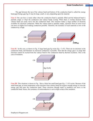
  • 1. The gap between the top of the valence band and bottom of the conduction band is called the energy band gap (Energy gap Eg). It may be large, small, or zero, depending upon the material.<br />Case I: One can have a metal either when the conduction band is partially filled and the balanced band is partially empty or when the conduction and valance bands overlap. When there is overlap electrons from valence band can easily move into the conduction band. This situation makes a large number of electrons available for electrical conduction. When the valence band is partially empty, electrons from its lower level can move to higher level making conduction possible. Therefore, the resistance of such materials is low or the conductivity is high.<br /> CB<br /> CB<br />VB VB Overlap<br /> <br />Case II: In this case, as shown in Fig. A large band gap Eg exists (Eg > 3 eV). There are no electrons in the conduction band, and therefore no electrical conduction is possible. Note that the energy gap is so large that electrons cannot be excited from the valence band to the conduction band by thermal excitation. This is the case of insulators.<br /> <br /> CB<br /> <br /> Eg(>3 eV)<br /> <br /> VB<br />Case III: This situation is shown in Fig. Here a finite but small band gap (Eg < 3 eV) exists. Because of the small band gap, at room temperature some electrons from valence band can acquire enough energy to cross the energy gap and enter the conduction band. These electrons (though small in numbers) can move in the conduction band. Hence, the resistance of semiconductors is not as high as that of the insulators.<br /> CB<br /> Eg(<3 eV)<br /> VB<br />Semiconductors<br />Based on the purity, semiconductors are classified into two types,<br />1. Intrinsic semiconductor and<br />2. Extrinsic semiconductor.<br />Intrinsic semiconductor<br />A semiconductor which is pure and contains no impurity is known as an intrinsic semiconductor. Example: pure germanium (Ge) and silicon (Si).<br /> Each Si and Ge atom is surrounded by four nearest neighbours. We know that Si and Ge have four valence electrons. In its crystalline structure, every Si or Ge atom tends to share one of its four valence electrons with each of its four nearest neighbour atoms, and also to take share of one electron from each such neighbour. These shared electrons pairs are referred to as forming a covalent bond.<br />Fig. Intrinsic semiconductor<br />As the temperature increases, more thermal energy becomes available to these electrons and some of these electrons may break–away (becoming free electrons contributing to conduction). The thermal energy effectively ionizes only a few atoms in the crystalline lattice and creates a vacancy in the bond. <br />The neighbourhood, from which the free electron (with charge –q) has come out leaves a vacancy with an effective charge (+q). This vacancy with the effective positive electronic charge is called a hole. The hole behaves as an apparent free particle with effective positive charge.<br />An intrinsic semiconductor will behave like an insulator at T = 0 K as shown in Fig. It is the thermal energy at higher temperatures (T > 0K), which excites some electrons from the valence band to the conduction band. These thermally excited electrons at T > 0 K, partially occupy the conduction band. Therefore, the energy-band diagram of an intrinsic semiconductor will be as shown in Fig. Here, some electrons are shown in the conduction band. These have come from the valence band leaving equal number of holes there.<br />In intrinsic semiconductors, the number of free electrons, ne is equal to the number of holes, nh. That is ne = nh = ni<br />Where ni is called intrinsic carrier concentration.<br />