
Recommended
More Related Content
Similar to 20EC402 - LIC - Unit-II - 09-02-2023.pptx
Similar to 20EC402 - LIC - Unit-II - 09-02-2023.pptx (20)
Recently uploaded
Recently uploaded (20)
20EC402 - LIC - Unit-II - 09-02-2023.pptx
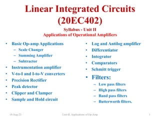
- 1. Linear Integrated Circuits (20EC402) Syllabus - Unit II Applications of Operational Amplifiers • Basic Op-amp Applications – Scale Changer – Summing Amplifier – Subtractor • Instrumentation amplifier • V-to-I and I-to-V converters • Precision Rectifier • Peak detector • Clipper and Clamper • Sample and Hold circuit • Log and Antilog amplifier • Differentiator • Integrator • Comparators • Schmitt trigger • Filters: – Low pass filters – High pass filters – Band pass filters – Butterworth filters. 18-Aug-23 Unit-II: Applications of Op-Amp 1
- 2. Operational Amplifier Applications • In linear circuits, the output signal varies with the input signal in a linear manner. • Applications: – Adder, – Subtractor, – V to I and I to V Converter, – Instrumentation Amplifier,… • In non-liner circuits, the outputs are varying highly non-linear with the inputs. • Applications: – Rectifier, – Peak Detector, – Clipper and Clamper, – SH circuit, – Log and Antilog amplifier,… 18-Aug-23 Unit-II: Applications of Op-Amp 2
- 3. Scale Changer/Inverter 18-Aug-23 Unit-II: Applications of Op-Amp 3 • Consider basic inv amplifier • If 𝑹𝒇 𝑹𝟏 = 𝑲 K is real constant • Then closed loop gain 𝑨𝑪𝑳 = − 𝑲 • For 𝑹𝒇 = 𝑹𝟏, 𝑨𝑪𝑳 = −𝟏 → the output is 1800 out of phase.
- 4. Summing Amplifier • Op-amp may be used to design a circuit whose output is the sum of several input signals is called summing amplifier or a summer. 18-Aug-23 Unit-II: Applications of Op-Amp 4 Inverting Summing Amplifier
- 5. Inverting Summing Amplifier 18-Aug-23 Unit-II: Applications of Op-Amp 5 Analysis, • Assume it is an ideal op-amp (𝑨𝑶𝑳 = ∞, 𝑹𝒊 = ∞ 𝒂𝒏𝒅 𝑰𝑩 = 𝟎) 𝑽𝒅𝒓𝒐𝒑(𝑹𝑪𝒐𝒎𝒑) = 𝟎 ∵ 𝑰𝑩 = 𝟎 • Hence Non-inv input is at ground potential. • Then, KCL at node ‘a’ is 𝑽𝟏 𝑹𝟏 + 𝑽𝟐 𝑹𝟐 + 𝑽𝟑 𝑹𝟑 + 𝑽𝟎 𝑹𝒇 = 𝟎 ⇒ 𝑽𝟎 = − 𝑹𝒇 𝑹𝟏 𝑽𝟏 + 𝑹𝒇 𝑹𝟐 𝑽𝟐 + 𝑹𝒇 𝑹𝟑 𝑽𝟑 • The output is an inverted, weighted sum of the inputs. • If, 𝑹𝟏 = 𝑹𝟐 = 𝑹𝟑 = 𝑹𝒇 ⇒ 𝑽𝟎 = − 𝑽𝟏 + 𝑽𝟐 + 𝑽𝟑 𝑹𝟏 = 𝑹𝟐 = 𝑹𝟑 = 𝟑𝑹𝒇 ⇒ 𝑽𝟎 = − 𝑽𝟏 + 𝑽𝟐 + 𝑽𝟑 𝟑 • Output is the average of the input signals(inverted). • To provide input bias current, 𝑹𝑪𝒐𝒎𝒑 can be find by , Make 𝑽𝟏 = 𝑽𝟐 = 𝑽𝟑 = 𝟎; Then effective input resistance 𝑹𝒊 = 𝑹𝟏 𝑹𝟐 𝑹𝟑 Then 𝑹𝑪𝒐𝒎𝒑 = 𝑹𝒊 𝑹𝒇 = 𝑹𝟏 𝑹𝟐 𝑹𝟑 𝑹𝒇
- 6. Non-Inverting Summing Amplifier • A summer that gives a non-inverted sum is the non-inverting summing amplifier. 18-Aug-23 Unit-II: Applications of Op-Amp 6 • Let voltage at inv & non-inv input terminal both are Va. • KCL at nod ‘a’ 𝑽𝟏−𝑽𝒂 𝑹𝟏 + 𝑽𝟐−𝑽𝒂 𝑹𝟐 + 𝑽𝟑−𝑽𝒂 𝑹𝟑 = 𝟎 ⟹ 𝑽𝒂 𝟏 𝑹𝟏 + 𝟏 𝑹𝟐 + 𝟏 𝑹𝟑 = 𝑽𝟏 𝑹𝟏 + 𝑽𝟐 𝑹𝟐 + 𝑽𝟑 𝑹𝟑 ⟹ 𝑽𝒂 = 𝑽𝟏 𝑹𝟏 + 𝑽𝟐 𝑹𝟐 + 𝑽𝟑 𝑹𝟑 𝟏 𝑹𝟏 + 𝟏 𝑹𝟐 + 𝟏 𝑹𝟑 • From diagram, 𝑽𝟎 = 𝟏 + 𝑹𝒇 𝑹 𝑽𝒂 = 𝟏 + 𝑹𝒇 𝑹 𝑽𝟏 𝑹𝟏 + 𝑽𝟐 𝑹𝟐 + 𝑽𝟑 𝑹𝟑 𝟏 𝑹𝟏 + 𝟏 𝑹𝟐 + 𝟏 𝑹𝟑 • Which is a non-inverted weighted sum of inputs. • Let 𝑹𝟏 = 𝑹𝟐 = 𝑹𝟑 = 𝑹 = 𝑹𝒇 𝟐 ⇒ 𝑽𝟎 = 𝑽𝟏 + 𝑽𝟐 + 𝑽𝟑
- 7. Subtractor • A basic differential amplifier can be used as a subtractor. • If all resistors are equal in value, then the output voltage can be derived by using superposition principle. 18-Aug-23 Unit-II: Applications of Op-Amp 7 • Output voltage due to V1 alone can be Vo1, make V2=0 then 𝑽𝟏 = 𝑽𝟏 𝟐 ∴ 𝑽𝒐𝟏 = 𝑽𝟏 𝟐 𝟏 + 𝑹 𝑹 = 𝑽𝟏 ⇒ 𝑽𝒐𝟏 = 𝑽𝟏 • Similarly, 𝑽𝒐𝟐 = −𝑽𝟐 • Output due to both inputs can be written as 𝑽𝒐 = 𝑽𝒐𝟏 + 𝑽𝒐𝟐 ⇒ 𝑽𝒐 = 𝑽𝟏 − 𝑽𝟐
- 8. Instrumentation Amplifier • Measuring and controlling of physical quantity is mandatory in industry, commercial applications. • Examples: – Temperature – Humidity – Light Intensity – Water Flow, etc., • Role of instrumentation Amplifier – Usually measured with transducers, output should be amplified for display or to drive the system. 18-Aug-23 Unit-II: Applications of Op-Amp 8
- 9. Instrumentation Amplifier • Important features of an instrumentation amplifier – High gain accuracy – High CMRR – High gain stability with low temperature coefficient. – Low DC offset – Low output impedance. • Special op-amps designed is μA725 • Monolithic Instrumentation amplifier commercially available are – AD521, AD524, AD624, – LH0036, LH0037, – INA104, 3626, 3629,… 18-Aug-23 Unit-II: Applications of Op-Amp 9
- 10. Instrumentation Amplifier • Consider a differential amplifier as 𝑽𝟎 = − 𝑹𝟐 𝑹𝟏 𝑽𝟐 + 𝟏 𝟏 + 𝑹𝟑 𝑹𝟒 𝑽𝟏 𝟏 + 𝑹𝟐 𝑹𝟏 ⟹ 𝑽𝟎 = − 𝑹𝟐 𝑹𝟏 𝑽𝟐 − 𝟏 𝟏 + 𝑹𝟑 𝑹𝟒 𝑽𝟏 𝑹𝟏 𝑹𝟐 + 𝟏 18-Aug-23 Unit-II: Applications of Op-Amp 10 For 𝑹𝟏 𝑹𝟐 = 𝑹𝟑 𝑹𝟒 ⟹ 𝑽𝟎 = − 𝑹𝟐 𝑹𝟏 𝑽𝟐 − 𝑽𝟏 • V1 seems input impedance = R3 + R4 = 101KΩ • V2 seems input impedance = R1 = 1KΩ • Low impedance leads the load the signal source heavily
- 11. • High resistance buffer is used as shown in figure 18-Aug-23 Unit-II: Applications of Op-Amp 11 Instrumentation Amplifier
- 12. • A, A2 have differential input voltage • for V1 = V2 , VR=0, – no current through R, R’ – A1, A2 acts as voltage follower , ⟹ 𝑽𝟐 ′ = 𝑽𝟐, 𝑽𝟏 ′ = 𝑽𝟏 18-Aug-23 Unit-II: Applications of Op-Amp 12 Instrumentation Amplifier • if V1≠ V2 , – current flows through R, R’ & – (V2 ’-V1 ’)>(V2-V1) has differential gain and more CMRR • Voltage at positive terminal of op-amp A3 is 𝑹𝟐𝑽𝟏 ′ 𝑹𝟏+𝑹𝟐 • Using super position theorem 𝑽𝟎 = − 𝑹𝟐 𝑹𝟏 𝑽𝟐 ′ + 𝟏 + 𝑹𝟐 𝑹𝟏 𝑹𝟐𝑽𝟏 ′ 𝑹𝟏 + 𝑹𝟐 ⇒ 𝑽𝟎 = 𝑹𝟐 𝑹𝟏 𝑽𝟏 ′ − 𝑽𝟐 ′
- 13. • Since no current flows into op-amp, Current flow upwards in R, and passes through R’ 𝑰 = 𝑽𝟏 − 𝑽𝟐 𝑹 𝑽𝟏 ′ = 𝑹′𝑰 + 𝑽𝟏 = 𝑹′ 𝑽𝟏 − 𝑽𝟐 𝑹 + 𝑽𝟏 18-Aug-23 Unit-II: Applications of Op-Amp 13 Instrumentation Amplifier 𝑽𝟐 ′ = −𝑹′ 𝑰 + 𝑽𝟐 = −𝑹′ 𝑽𝟏 − 𝑽𝟐 𝑹 + 𝑽𝟐 • We know that, 𝑽𝟎 = 𝑹𝟐 𝑹𝟏 𝑽𝟏 ′ − 𝑽𝟐 ′ = 𝑹𝟐 𝑹𝟏 𝑹′ 𝑽𝟏−𝑽𝟐 𝑹 + 𝑽𝟏 + 𝑹′ 𝑽𝟏−𝑽𝟐 𝑹 − 𝑽𝟐 𝑽𝟎 = 𝑹𝟐 𝑹𝟏 𝟐𝑹′ 𝑹 𝑽𝟏 − 𝑽𝟐 + 𝑽𝟏 − 𝑽𝟐 𝑽𝟎 = 𝑹𝟐 𝑹𝟏 𝟏 + 𝟐𝑹′ 𝑹 𝑽𝟏 − 𝑽𝟐 𝑽𝟎 ∝ 𝑹
- 14. Instrumentation Amplifier using Transducer Bridge • The bridge is initially balanced for Vdc, V1=V2 • When physical quantity changes, RT changes, V1≠V2 • This differential voltage is amplified by 3 op-amp. 18-Aug-23 Unit-II: Applications of Op-Amp 14
- 15. V to I and I to V converter V to I Converter (Transconductance Amplifier) • Op-amp can convert a voltage signal to a proportional output current. (Types: 1). V-I converter with Floating load, 2). Grounded load) 18-Aug-23 Unit-II: Applications of Op-Amp 15 • Floating load ZL (wkt, Va = Vi), 𝑽𝒊 = 𝒊𝑳𝑹𝟏 ∵ 𝑰𝑩 − = 𝟎 ⇒ 𝒊𝑳 = 𝑽𝒊 𝑹𝟏 • The input voltage is converted into an output current of 𝑽𝒊 𝑹𝟏
- 16. 18-Aug-23 Unit-II: Applications of Op-Amp 16 • From diagram (Va = V1) • By KCL 𝒊𝟏 + 𝒊𝟐 = 𝒊𝑳 ⇒ 𝑽𝒊 − 𝑽𝟏 𝑹 + 𝑽𝒐 − 𝑽𝟏 𝑹 = 𝒊𝑳 ⇒ 𝑽𝒊 + 𝑽𝒐 − 𝟐𝑽𝟏 = 𝒊𝑳𝑹 ⇒ 𝑽𝟏 = 𝑽𝒊 + 𝑽𝒐 − 𝒊𝑳𝑹 𝟐 V to I Converter (Transconductance Amplifier) 𝒘𝒌𝒕, 𝑨𝑪𝑳 = 𝟏 + 𝑹𝒇 𝑹𝟏 = 𝟏 + 𝑹 𝑹 = 𝟐 ⇒ 𝑽𝒐 𝑽𝟏 = 𝟐 ⇒ 𝑽𝒐 = 𝟐𝑽𝟏 𝑽𝟏 = 𝑽𝒊 + 𝑽𝒐 − 𝒊𝑳𝑹 𝟐 ⇒ 𝑽𝒐 = 𝟐𝑽𝟏 = 𝑽𝒊 + 𝑽𝒐 − 𝒊𝑳𝑹 ⇒ 𝑽𝒊 = 𝒊𝑳𝑹 ⇒ 𝒊𝑳 = 𝑽𝒊 𝑹𝟏 • V to I converter is used for low voltage dc and ac voltmeter, LED and Zener Diode tester.
- 17. I to V Converter (Transresistance amplifier) • Photocell, photodiode and photovoltaic cell give an output current that is proportional to an incident radiant energy or light, these current can be converted to voltage by using these I to V converter. 18-Aug-23 Unit-II: Applications of Op-Amp 17 • Here -ve input terminal is virtual grounded, – no current through Rs and – Is flows through Rf, then 𝑽𝟎 = −𝑰𝒔𝑹𝑭 • Hence it can detect lower current. • Sometimes, Rf shunted with a Cf to reduce high frequency noise and oscillations
- 18. Op-Amp Circuits using Diodes • The major limitation of ordinary diode is, it cannot rectify voltage below 𝑽𝜸 𝟎. 𝟔𝑽 , the cut-in voltage of the diode. • When a diode is placed in a feedback loop of an op-amp it can act as ideal diode. 18-Aug-23 Unit-II: Applications of Op-Amp 18 • 𝑽𝜸 𝟎. 𝟔𝑽 is virtually eliminated due to it is divided by the open loop gain 𝑨𝑶𝑳 ~𝟏𝟎𝟒 . • When 𝑽𝒊 > 𝑽𝜸 𝑨𝑶𝑳 𝒊𝒆, . 𝟎.𝟔 𝟏𝟎𝟒 = 𝟔𝟎𝝁𝑽 ⇒ 𝑽𝒐𝑨(ie, when Diode D conducts when 𝑽𝒐𝑨 > 𝑽𝜸 → Voltage Follower. • Ie,. Vo follows Vi during +ve half cycle.
- 19. • When Vi is –ve or 𝑽𝒊 < 𝑽𝜸 𝑨𝑶𝑳 D is off , no current is delivered to IL (except less IBias, ID-Saturation) • This circuit is called Precision rectifier. • Applications: – Half-wave rectifier – Full-wave rectifier – Peak-value detector – Clipper – Clamper 18-Aug-23 Unit-II: Applications of Op-Amp 19 Op-Amp Circuits using Diodes
- 20. Half-Wave Rectifier 18-Aug-23 Unit-II: Applications of Op-Amp 20 • An inv-op-amp can be converted to half-wave rectifier using two diodes • When Vi is positive(Vi>0), D1 conducts, VoA is negative, D2 Reverse Bias, V0 is zero. (Becaues input current flows through D1 & no current flows through RF) • When Vi<0, D2 conducts, D1 is off, VoA is positive, the circuit acts as inverter for Rf=R1 and V0 is positive. • Limitaion : Slew rate of the op-amp. • The circuit provides positive output. • If both diodes are reversed, then +ve input signal is transmitted and gets inverted then output is negative.
- 21. Full-Wave Rectifier 18-Aug-23 Unit-II: Applications of Op-Amp 21 • Also called absolute value circuit. • For Vi>0, • D1 is on and • D2 is off. • Both op-amps A1 and A2 act as inverter as in equivalent circuit. • Here V0 = Vi • For Vi<0, • D1 is off and • D2 is on.
- 22. 18-Aug-23 Unit-II: Applications of Op-Amp 22 Full-Wave Rectifier • Let output of A1 be V, also differential input at A2=0, Voltage at inv input is V. • KCL at node ‘a’ is 𝑽𝒊 𝑹 + 𝑽 𝟐𝑹 + 𝑽 𝑹 = 𝟎 ⇒ 𝑽 = − 𝟐 𝟑 𝑽𝒊 • The equivalent circuit is a non-in amplifier 𝑽𝟎 = 𝟏 + 𝑹 𝟐𝑹 − 𝟐 𝟑 𝑽𝒊 = 𝑽𝒊 • For Vi<0, the output is positive. The input and output waveforms are as in figure. • This circuit is also called an absolute value circuit as output is positive even when input is negative. • It is possible to obtain negative outputs for either polarity of input simply reversing the diodes.
- 23. Peak Detector 18-Aug-23 Unit-II: Applications of Op-Amp 23 • If Vi > VC then diode is forward biased, act as voltage follower, V0 = Vi • When Vi < VC, then diode is reverse biased, capacitor holds the charge till Vi > VC. • Reset when VC = 0 , made by connecting low leakage MOSFET switch across the capacitor • Lowest or negative peak can be detected by reversing the diode. • Applications: • Test, • Measurement and instrumentation, • Amplitude modulation in communications • Function is to compute the peak value of input • The circuit follows – The voltage peaks of signal and stores the highest value on a capacitor. – If highest peak signal value comes, the new value is stored. – Highest peak value is stored until capacitor discharges
- 24. Clipper 18-Aug-23 Unit-II: Applications of Op-Amp 24 • A precision diode may used to clip- off a certain position of input. • Clipping level is determined by Vref.. • Vi is given to positive input • When V0 > Vref then clipped off – Up to Vi≤ Vref , diode conducts because opamp will act as voltage follower (V0 = Vi) – When Vi > Vref , diode cut-off , opamp is open loop , V0 = Vref • If Vref is negative – V0 above Vref will be clipped off
- 25. Clipper 18-Aug-23 Unit-II: Applications of Op-Amp 25 • Positive clipper simply converted to negative clipper by simply reversing diode D and changing the polarity of Vref. • It clips off the negative parts of input when < Vref • Negative clipper circuit
- 26. Clamper • Also known as dc inserter (or) restorer. • The circuit used to add desired dc level to V0. – So output is clamped to desired level. • In positive clamper, – clamped dc level is positive • In negative clamper, – clamped dc level is negative. • A variable positive dc voltage is given at positive input • This circuit clamps the peaks of input waveform so called peak clamper. • Output is the net result of ac and dc input applied to negative and positive. 18-Aug-23 Unit-II: Applications of Op-Amp 26
- 27. • If Vref at positive terminal then – Vref is +ve → V’ is +ve , → diode D is forward biased, so it acts as voltage follower, V0 = +Vref. • Let Vi = Vm sinωt at negative input terminal – In negative half cycle of Vi , diode D conducts (FB), C1 charges through D to Vm (negative peak voltage) – In positive half cycle of Vi , D is reverse biased, C1 retains Vm (previous voltage) • But Vm is in series with ac input signal, then output = Vi +Vm • Total output = Vref + Vi + Vm • Negative peak clamping by reversing diode and negative reference voltage. 18-Aug-23 Unit-II: Applications of Op-Amp 27 Clamper
- 28. Sample and Hold Circuit • Samples, an input signal and holds on to its last sampled value until the input is sampled again. • Applications: – Digital interfacing – Analog to digital – Pulse code modulation systems • The simplest sample and hold circuit is 18-Aug-23 Unit-II: Applications of Op-Amp 28 • MOSFET works as a switch (controlled by control voltage Vc) • Capacitor stores the charge. • Vi to be sampled is applied to drain of MOSFET and Vc applied to gate.
- 29. 18-Aug-23 Unit-II: Applications of Op-Amp 29 Sample and Hold Circuit • When Vc is positive MOSFET turns on, capacitor charges as Vi. – Time constant = R0 + rds (ON) – R0 → output resistance of A1 (voltage follower) – rds (ON) → resistance of MOSFET when ON. • Vi appears across C and output of A2 (voltage follower) • When Vc = 0 → MOSFET is OFF – But C discharges to A2 , have highest input impedance, so C holds the voltage across it. – Ts → sample period (during which VC = Vi) – TH → Hold period (during which VC = constant) • Frequency of VC should be higher , at least twice the input voltage, to retrieve the input from output
- 30. Log Amplifier 18-Aug-23 Unit-II: Applications of Op-Amp 30 • Grounded base transistor is placed in FB path since collector is virtual grounded, and base is also grounded • Transistor acts as diode 𝑰𝑪 = 𝑰𝑬 = 𝑰𝑺 𝒆 𝒒𝑽𝑬 𝑲𝑻 − 𝟏 Where, IS → emitter saturation current ≈10-3A K → Boltzmann’s constant T → Absolute temperature in (0K) 𝑰𝑪 𝑰𝑺 = 𝒆 𝒒𝑽𝑬 𝑲𝑻 − 𝟏 ⇒ 𝒆 𝒒𝑽𝑬 𝑲𝑻 = 𝑰𝑪 𝑰𝑺 + 𝟏 ≈ 𝑰𝑪 𝑰𝑺 • Taking natural log on both sides 𝒒𝑽𝑬 𝑲𝑻 = 𝒍𝒏 𝑰𝑪 𝑰𝑺 ⇒ 𝑽𝑬 = 𝑲𝑻 𝒒 𝒍𝒏 𝑰𝑪 𝑰𝑺
- 31. Log Amplifier 18-Aug-23 Unit-II: Applications of Op-Amp 31 • From figure 𝑰𝑪 = 𝑽𝒊 𝑹𝟏 , 𝑽𝑬 = −𝑽𝟎, 𝑽𝑬 = 𝑲𝑻 𝒒 𝒍𝒏 𝑰𝑪 𝑰𝑺 𝑽𝟎 = − 𝑲𝑻 𝒒 𝒍𝒏 𝑽𝒊 𝑹𝟏𝑰𝑺 ⇒ 𝑽𝟎 = − 𝑲𝑻 𝒒 𝒍𝒏 𝑽𝒊 𝑽𝒓𝒆𝒇 Where, 𝑽𝒓𝒆𝒇 = 𝑹𝟏𝑰𝑺 • Output voltage is proportional to logarithm of input voltage • We know that, log10X = 0.4343lnX • Drawback – IS varies transistor to transistor and with temperature – Vref cannot be obtained
- 32. • Drawback This can be eliminated by the circuit as • Here input applied to one log-amplifier and reference applied to another log-amplifier • Integrated in same silicon wafer • Provides a close match of saturation currents and ensures good thermal tracking. 18-Aug-23 Unit-II: Applications of Op-Amp 32 Log Amplifier
- 33. • Assume𝑰𝑺𝟏 = 𝑰𝑺𝟐 = 𝑰𝑺 𝑽𝟏 = − 𝑲𝑻 𝒒 𝒍𝒏 𝑽𝒊 𝑹𝟏𝑰𝑺 ; 𝑽𝟐 = − 𝑲𝑻 𝒒 𝒍𝒏 𝑽𝒓𝒆𝒇 𝑹𝟏𝑰𝑺 𝑽𝟎 = 𝑽𝟐 − 𝑽𝟏 = 𝑲𝑻 𝒒 𝒍𝒏 𝑽𝒊 𝑹𝟏𝑰𝑺 − 𝒍𝒏 𝑽𝒓𝒆𝒇 𝑹𝟏𝑰𝑺 ⇒ 𝑽𝟎 = 𝑲𝑻 𝒒 𝒍𝒏 𝑽𝒊 𝑽𝒓𝒆𝒇 • Reference can be set by single voltage source but output voltage(V0) is proportional to T, this can be compensated by the last stage op-amp (A4) provides non-inverting 𝒈𝒂𝒊𝒏 = 𝟏 + 𝑹𝟐 𝑹𝑻𝑪 𝑽𝟎 𝑪𝒐𝒎𝒑 = 𝟏 + 𝑹𝟐 𝑹𝑻𝑪 𝑲𝑻 𝒒 𝒍𝒏 𝑽𝒊 𝑽𝒓𝒆𝒇 – RTC is a temperature sensitive resistance 18-Aug-23 Unit-II: Applications of Op-Amp 33 Log Amplifier
- 34. Antilog Amplifier • Input Vi is fed into temperature compensating voltage divider R2 & RTC , to base of Q2 • V0 is feedback to inverting input A1 through resistor R1 • The base –Emitter voltage of Q1, Q2 can be written as 𝑽𝑸𝟏 𝑩−𝑬 = − 𝑲𝑻 𝒒 𝒍𝒏 𝑽𝟎 𝑹𝟏𝑰𝑺 𝑽𝑸𝟐 𝑩−𝑬 = − 𝑲𝑻 𝒒 𝒍𝒏 𝑽𝒓𝒆𝒇 𝑹𝟏𝑰𝑺 18-Aug-23 Unit-II: Applications of Op-Amp 34
- 35. Antilog Amplifier • Since the base of Q is tied ground 𝑽𝑨 = −𝑽𝑸𝟏 𝑩−𝑬 = − 𝑲𝑻 𝒒 𝒍𝒏 𝑽𝟎 𝑹𝟏𝑰𝑺 • Base voltage VB of Q2 is 𝑽𝑩 = 𝑹𝑻𝑪 𝑹𝟐 + 𝑹𝑻𝑪 𝑽𝒊 • Emitter voltage of Q2 𝑽𝑸𝟐𝑬 = 𝑽𝑩 + 𝑽𝑸𝟐 𝑩−𝑬 𝑽𝑸𝟐𝑬 = 𝑹𝑻𝑪 𝑹𝟐 + 𝑹𝑻𝑪 𝑽𝒊 − 𝑲𝑻 𝒒 𝒍𝒏 𝑽𝒓𝒆𝒇 𝑹𝟏𝑰𝑺 • Emitter voltage of Q2=VA = VQ2E 18-Aug-23 Unit-II: Applications of Op-Amp 35 − 𝑲𝑻 𝒒 𝒍𝒏 𝑽𝟎 𝑹𝟏𝑰𝑺 = 𝑹𝑻𝑪 𝑹𝟐 + 𝑹𝑻𝑪 𝑽𝒊 − 𝑲𝑻 𝒒 𝒍𝒏 𝑽𝒓𝒆𝒇 𝑹𝟏𝑰𝑺 𝑹𝑻𝑪 𝑹𝟐 + 𝑹𝑻𝑪 𝑽𝒊 = − 𝑲𝑻 𝒒 𝒍𝒏 𝑽𝟎 𝑹𝟏𝑰𝑺 − 𝒍𝒏 𝑽𝒓𝒆𝒇 𝑹𝟏𝑰𝑺 − 𝑹𝑻𝑪 𝑹𝟐 + 𝑹𝑻𝑪 𝒒 𝑲𝑻 𝑽𝒊 = 𝒍𝒏 𝑽𝟎 𝑽𝒓𝒆𝒇
- 36. Antilog Amplifier • Change from ln to log10. −𝟎. 𝟒𝟑𝟒𝟑 𝑹𝑻𝑪 𝑹𝟐 + 𝑹𝑻𝑪 𝒒 𝑲𝑻 𝑽𝒊 = 𝟎. 𝟒𝟑𝟒𝟑 𝒍𝒏 𝑽𝟎 𝑽𝒓𝒆𝒇 −𝑲′𝑽𝒊 = 𝒍𝒐𝒈 𝑽𝟎 𝑽𝒓𝒆𝒇 𝑾𝒉𝒆𝒓𝒆, 𝑲′ = 𝟎. 𝟒𝟑𝟒𝟑 𝑹𝑻𝑪 𝑹𝟐 + 𝑹𝑻𝑪 𝒒 𝑲𝑻 ⟹ 𝑽𝟎 𝑽𝒓𝒆𝒇 = 𝟏𝟎−𝑲′𝑽𝒊 ⟹ 𝑽𝟎 = 𝑽𝒓𝒆𝒇 𝟏𝟎−𝑲′𝑽𝒊 18-Aug-23 Unit-II: Applications of Op-Amp 36 • When Input increased by one voltage, output decreased by decade. • 755 log/antilog amplifier IC chip is available as functional module.
- 37. Differentiator • The op-amp circuits that contain capacitor is the differentiating amplifier or differentiation. • The output waveform is the derivative of the input waveform. Analysis • The node ‘N’ is at virtual ground potential (VN=0), then 𝒊𝑪 = 𝑪𝟏 𝒅 𝒅𝒕 𝑽𝒊 − 𝑽𝑵 = 𝑪𝟏 𝒅𝑽𝒊 𝒅𝒕 • The current through feedback Resistor, 𝒊𝑭 = 𝑽𝒐 𝑹𝑭 & no current into the op-amp. 18-Aug-23 Unit-II: Applications of Op-Amp 37 • By KCL at node N is 𝑪𝟏 𝒅𝑽𝒊 𝒅𝒕 + 𝑽𝟎 𝑹𝑭 = 𝟎 ⇒ 𝑽𝟎 = −𝑹𝑭𝑪𝟏 𝒅𝑽𝒊 𝒅𝒕 • The minus sign indicates 1800 phase shift of the output wrt to input signal. • In phasor equivalent 𝑽𝟎 𝒔 = −𝑹𝑭𝑪𝟏𝒔𝑽𝒊 𝒔 • In steady state 𝒔 = 𝒋𝝎. • The magnitude of gain A is 𝑨 = 𝑽𝟎 𝑽𝒊 = −𝒋𝝎𝑹𝑭𝑪𝟏 = 𝝎𝑹𝑭𝑪𝟏 = 𝒇 𝒇𝒂 Where, 𝒇𝒂 = 𝟏 𝟐𝝅𝑹𝑭𝑪𝟏 • At 𝒇 = 𝒇𝒂, 𝑨 = 𝟏, i.e., 0dB and gain increases at rate of +20 dB/decade.
- 38. • At high frequency, differentiator become unstable, the input impedance decreases, this leads sensitive to high frequency noise. • Hence, 18-Aug-23 Unit-II: Applications of Op-Amp 38 Differentiator
- 39. Integrator • Integrating both the sides, 𝟎 𝒕 𝒅𝑽𝟎 = − 𝟏 𝑹𝟏𝑪𝑭 𝟎 𝒕 𝑽𝒊𝒅𝒕 ⇒ 𝑽𝟎 𝒕 = − 𝟏 𝑹𝟏𝑪𝑭 𝟎 𝒕 𝑽𝒊 𝒕 𝒅𝒕 + 𝑽𝟎 𝟎 • Where, V0(0) is the initial output voltage. • Due to negative sign in the output it can also known as an inverting integrator. • Rcomp is connected to minimize the effect of input bias current. • In phasor notation, 𝑽𝟎 𝒔 = − 𝟏 𝒔𝑹𝟏𝑪𝑭 𝑽𝒊 𝒔 • In steady state 𝒔 = 𝒋𝝎 ⇒ 𝑽𝟎 𝒋𝝎 = − 𝟏 𝒋𝝎𝑹𝟏𝑪𝑭 𝑽𝒊 𝒋𝝎 • The magnitude of gain A is 𝑨 = 𝑽𝟎 𝒋𝝎 𝑽𝒊 𝒋𝝎 = − 𝟏 𝒋𝝎𝑹𝟏𝑪𝑭 = 𝟏 𝝎𝑹𝟏𝑪𝑭 18-Aug-23 Unit-II: Applications of Op-Amp 39 • If the resistor and capacitor of the differentiator is interchanged, we can obtain the integrator. • By KCL at node N is 𝑽𝒊 𝑹𝟏 + 𝑪𝑭 𝒅𝑽𝟎 𝒅𝒕 = 𝟎 ⇒ 𝒅𝑽𝟎 𝒅𝒕 = − 𝑽𝒊 𝑹𝟏𝑪𝑭
- 40. Integrator 18-Aug-23 Unit-II: Applications of Op-Amp 40 • Frequency response (or Bode Plot) of this basic integrator is, • At 𝒇 = 𝒇𝒃 𝒇𝒃 = 𝟏 𝟐𝝅𝑹𝟏𝑪𝑭 gain of the integrator is 0dB • At lower frequency the gain becomes infinite, hence the feedback capacitor is shunted by a RF to avoid saturation or infinity. • The parallel combination of RF and CF, dissipates power, so it is called ‘Lossy Integrator’
- 41. Comparator Introduction • Op-amp in open loop will act in nonlinear manner. • Application: – Comparators – Detectors – Limiters – Digital interfacing devices (converters) Comparators • Compares a signal voltage applied at one input with known reference at another input. i.e., 𝑽𝟎 = ±𝑽𝑺𝒂𝒕(𝒊𝒅𝒆𝒂𝒍 𝒄𝒉𝒂𝒓𝒂𝒄𝒕𝒆𝒓𝒊𝒔𝒕𝒊𝒄𝒔) • Types: – Non-inverting comparator – Inverting comparator 18-Aug-23 Unit-II: Applications of Op-Amp 41
- 42. Non-Inverting Comparator • When reference given at negative input and time varying signal(Vi)-input is applied at positive input. 𝑽𝟎 = −𝑽𝒔𝒂𝒕 𝒇𝒐𝒓 𝑽𝒊 < 𝑽𝒓𝒆𝒇 𝒔𝒊𝒎𝒊𝒍𝒂𝒓𝒍𝒚, 𝑽𝟎 = +𝑽𝒔𝒂𝒕 𝒇𝒐𝒓 𝑽𝒊 > 𝑽𝒓𝒆𝒇 18-Aug-23 Unit-II: Applications of Op-Amp 42
- 43. • Here reference given at positive input and time varying signal(Vi)-input is at negative input. • The practical comparator has the output obtained by zener diode. • A resistance (limiting the current) and two back to back zener diodes at output. • The output limiting voltages are 𝑽𝒁𝟏 + 𝑽𝑫 𝒂𝒏𝒅 − 𝑽𝒁𝟐 + 𝑽𝑫 – 𝒘𝒉𝒆𝒓𝒆, 𝑽𝑫 ≅ 𝟎. 𝟕𝑽 𝒊. 𝒆. , 𝒅𝒊𝒐𝒅𝒆 𝒇𝒐𝒓𝒎𝒘𝒂𝒓𝒅 𝒗𝒐𝒍𝒕𝒂𝒈𝒆 18-Aug-23 Unit-II: Applications of Op-Amp 43 Non-Inverting Comparator
- 44. • Above waveform shown are the instantaneous. • Practically it takes certain amount of time to switch from one voltage to another voltage level. • If 741 internally compensated is used as comparator, primary limitation is slew rate. • Uncompensated op-amp make faster comparators than compensated op-amps. • Application of comparator: – Zero Crossing Detector – Window Detector – Time Marker Generator – Phase meter. 18-Aug-23 Unit-II: Applications of Op-Amp 44 Non-Inverting Comparator
- 45. Zero Crossing Detectors • Basic comparators can be used as zero crossing detectors. • Due to input is sine wave, output is square wave it is called as square wave generator. 18-Aug-23 Unit-II: Applications of Op-Amp 45
- 46. Window Detector 18-Aug-23 Unit-II: Applications of Op-Amp 46 • Mark the instant at which an unknown instant is between two threshold levels is called window detector. • Three indicators, – Yellow (LED-3) for <3V too low – Green (LED-2) for3-6V for safe input – Red (LED-1) for>6V high input
- 47. Time Marker Generator • Output of zero crossing detector (ZCD) is differentiated by an RC circuit (RC << T) – Then V’ is series positive and negative pulses. – After passing diode D, negative portion clipped off. • Sinusoidal wave has been converted into train of positive pulses spacing T. • Used in triggering of Monoshots, SCR, Sweep voltage of CRT etc,. 18-Aug-23 Unit-II: Applications of Op-Amp 47
- 48. Phase Detector • Phase angle between two voltages can also be measured using circuit is called marker generator. Both voltages are converted to spikes Time interval between pulse spike is measured. Time interval depends on phase difference (can measure from (00 to 3600) 18-Aug-23 Unit-II: Applications of Op-Amp 48
- 49. Regenerative Comparator (Schmitt Trigger) • If positive feedback added to comparator then gain is increase greatly. • Theoretically, if loop gain (-βAOL) is adjusted to unity, then gain with feedback(AVF) becomes infinite, but output is extreme. • Therefore, practical circuits cannot maintain loop gain unity because of supply voltage and temperature variations, so greater than unity is chosen. • Now output is discontinuous • This phenomenon called hysteresis (or) backlash. 18-Aug-23 Unit-II: Applications of Op-Amp 49
- 50. 18-Aug-23 Unit-II: Applications of Op-Amp 50 Regenerative Comparator (Schmitt Trigger)
- 51. • Regenerative comparator (above) called Schmitt trigger – Input given to negative terminal – Feedback given to positive terminal • The input vi triggers the output V0, when every time exceeds certain voltage levels – Then Upper Threshold Voltage VUT – Lower Threshold Voltage VLT • The hysteresis width is difference between two threshold VUT - VLT • Can be calculated as – When V0 = +VSat , then voltage at positive input terminal will be 𝑽𝒓𝒆𝒇 + 𝑹𝟐 𝑹𝟏 + 𝑹𝟐 𝑽𝒔𝒂𝒕 − 𝑽𝒓𝒆𝒇 = 𝑽𝑼𝑻 • 𝑾𝒉𝒆𝒏 𝑽𝒊 < 𝑽𝑼𝑻 → 𝑽𝟎 = +𝑽𝒔𝒂𝒕 • 𝑾𝒉𝒆𝒏 𝑽𝒊 > 𝑽𝑼𝑻 → 𝑽𝟎 = −𝑽𝒔𝒂𝒕 18-Aug-23 Unit-II: Applications of Op-Amp 51 Regenerative Comparator (Schmitt Trigger)
- 52. • Regenerativly switches are remains up to Vi > VUT – for V0 = -Vsat , – voltage at positive terminal is 𝑽𝒓𝒆𝒇 − 𝑹𝟐 𝑹𝟏+𝑹𝟐 𝑽𝒔𝒂𝒕 + 𝑽𝒓𝒆𝒇 = 𝑽𝑳𝑻 • When Vi < VLT (to switch) V0= -Vsat to +Vsat (regenerative transition take place) • Usually VLT < VUT • difference between these two are known as hysteresis (VH) 𝑽𝑯 = 𝑽𝑼𝑻 − 𝑽𝑳𝑻 = 𝟐𝑹𝟐𝑽𝒔𝒂𝒕 𝑹𝟏 + 𝑹𝟐 • Therefore, VH is independent of Vref • To compensate input bias current 𝑹𝟑 = 𝑹𝟏 𝑹𝟐 • For non-inverting Schmitt trigger Vi, Vref are interchanged • Important application of Schmitt trigger circuit is to convert very slowly varying input voltage into square wave output. 18-Aug-23 Unit-II: Applications of Op-Amp 52 Regenerative Comparator (Schmitt Trigger)
- 53. First and Second Order Active Filter Electric filters: • Separation of signals according to their frequencies • Widely used in communication, signal processing • Filters can be built from 1). Passive RLC components 2). Crystals (or) 3). Resistors, Capacitors & op-amp (active filters) RC Active Filters • In frequency selective circuits the circuit passes signals of specified band of frequency and attunates the signals outside the band is called Electric filter • Type 1). Analog, 2). Digital • Simplest way is using R,L,C • Suitable for high frequencies(radio frequency) 18-Aug-23 Unit-II: Applications of Op-Amp 53
- 54. First and Second Order Active Filter • Active filters uses op-amp as active element R,C as passive elements • Op-amp is non-inv mode, offer high input impedance and low output impedance, provide high load drive capacity. • Limitations of active filters – High frequency response is limited by gain BW (GBW) product(X) and slew rate of op-amp – High frequency active filters are more expensive. • Commonly used filters are – Low Pass Filter (LPF) – High Pass Filter (HPF) – Band Pass Filter (BPF) • Band Reject Filter / Band Stop Filter (BSF) 18-Aug-23 Unit-II: Applications of Op-Amp 54
- 55. 18-Aug-23 Unit-II: Applications of Op-Amp 55