SlideShare a Scribd company logo
1 of 52
OP AMP
“It is direct coupled high gain negative feed back amplifier”
- which perform mathematical operations like, addition, subtraction ,
multiplication and division.
- Which consists of amplifiers, level translators and output driver.
SYMBOL OF OP-AMP:
V1 – inverting input(-)
V2 - non inverting input(+)
V0 – the final output.
PIN DIAGRAM OF OP –AMP:
- it is a 8 pin IC with pin number of 741.
- the input operating voltage is +13 to -13V.
1st & 5th pin- offset null- used to nullify the output.
2nd pin- inverting input- used to give the inverting input
3rd pin- non inverting input- used to give the non inverting input
4th & 7th pin- +Vcc & -Vcc- used to apply the positive and negative input supply.
6th pin- output- used to drive the output voltage.
8th pin- no connection- application not yet assigned
BLOCK DIAGRAM OF OP AMP:
“ It is a four stage operational amplifier”
Which consists of i) input stage- differential amplifier
ii) intermediate stage- voltage amplifier
iii) level shifting stage- level translator
iv) output stage- output driver
i) differential amplifier- which produce the two differential output with high input impedance
ii) voltage amplifier- which produce the single ended amplified output
iii) level translator- it is used to translate the dc level at the output downwards to zero
iv) output driver- used to increases the output voltage swing and current supplying capability
CHARACTERISTICS OF OP AMP:
1. high input impedance Ri=∞
2. low output impedance R0= 0
3. high bandwidth BW= ∞
4. perfect balance V0= 0
Parameters of op-amp:
1)Input offset Voltage- it is the voltage that must be applied between the two
input terminals of an op-amp to null the output.
2) Input offset current- The algebraic difference between the current in the
inverting and non inverting terminal
3) Input Bias Current- it is the average current flows in the inverting and non-
inverting terminal of an op amp.
4) Large Signal Voltage gain- It is the ratio of the output voltage and the
differential input voltage[ Vo/Vid]
5) Output Voltage Swing- which indicates the values of positive and negative
saturation voltage of the op-amp. For 741 IC, it is +13 and -13V.
6) Differential input resistance Ri- it is the equivalent resistance that can be
measured at either the inverting or non-inverting input terminals with the other
terminal connected to ground.(2Mohm).
7) Input Capacitance Ci- it is the equivalent capacitance that can be measured
at either the
inverting or non-inverting input terminal with the other terminal connected to
ground.(1.4 pF).
8) Common Mode Rejection Ratio(CMRR)- It is defined as the ratio of the
differential mode voltage gain (Ad) and common mode voltage gain. CMRR =
Ad/Acm
9) Supply voltage Rejection Ratio- The change in an op-amps input offset voltage
Vio caused by variations in the supply voltage is called the SVRR. SR= ΔVio/ΔV
10) Slew Rate- it is defined as the maximum rate of change of output voltage per
unit of time and is expressed as volts per micro second.
VIRTUAL GROUND
“In op-amp, The non inverting terminal is connected to ground but the inverting terminal
is not directly connected to ground. But it acts like a ground terminal. Therefore the
inverting terminal is said to be at virtual ground”
“the differential input voltage is ideally zero, that is the voltage at the inverting terminal
V1 is approximately equal to that at the non inverting terminal V2.”
ADVANTAGES OF OP-AMP
i) Inexpensive
ii) Versatile
iii) Easy to use
APPLICATIONS OF OP-AMP
i) Used in negative amplifiers.
ii) Used in wave shaping circuits
iii) Used in filter circuit
iv) Used in many mathematical operations.
(a)inverting amplifier
(b)non-inverting amplifier
(c) summing amplifier
(d) integrator
(e) differentiator
(f) Voltage follower.
(g) Comparator
(h) Zero crossing detector,etc
INVERTING AMPLIFIER:
“ It is an amplifier which shift phase of the input signal by 180 degree”
- op amp 741 IC is used with power supply +Vcc & -Vcc.
- the non inverting terminal is grounded.
- the input voltage Vi is applied to inverting terminal through
input resistance Ri.
- the feedback resistance Rf is connected between Vs and Vo.
- the output voltage measured from Vo.
Applying Kirchhoff's current law,
Vo= -Vi(Rf/Ri); Vo= -Vi.Av; hence voltage gain Av= Rf/Ri
From the above equation, the input voltage is inverted at the output side has been proved.
NON INVERTING AMPLIFIER:
“ It is an amplifier which does not shift the phase of the input signal”
- op amp 741 IC is used with power supply +Vcc & -Vcc.
- the inverting terminal is grounded through input resistance Ri.
- the input voltage Vi is applied to non inverting terminal.
- the feedback resistance Rf is connected between Vs and Vo.
- the output voltage measured from Vo.
Applying Kirchhoff's current law,
Vo= Vi.Av; hence voltage gain Av= (1+Rf/Ri )
From the above equation, the input voltage does not
inverted at the output side has been proved.
SUMMING AMPLIFIER:
“ It is an amplifier which add all the input voltage with phase shift” ”it is also known
as voltage adder”
- op amp 741 IC is used with power supply +Vcc & -Vcc.
- the non inverting terminal is grounded.
- the input voltages V1,V2&V3 are applied to inverting terminal through
input resistances R1,R2&R3.
- the feedback resistance Rf is connected between Vs and Vo.
- the output voltage measured from Vo.
Applying Kirchhoff's current law,
From the above equation, the input voltages are added inverted at the output side
has been proved.
VOLTAGE FOLLOWER:
“ It is an amplifier which follows the input voltage with unity gain ”
- op amp 741 IC is used with power supply +Vcc & -Vcc.
- the input voltage Vi is applied to non inverting terminal.
- the inverting terminal is connected with Vo directly.
- the output voltage measured from Vo.
From the non inverting amplifier,
here, Rf & Ri = 0;
Vo = (1+0)Vi
Vo = (1)Vi
Vo = Vi
From the above equation, the output voltage follows the input voltage with
unity gain has been proved.
COMPARATOR:
“ It is a comparator which is used to compare the two input voltages ”
- op amp 741 IC is used with power supply +Vcc & -Vcc.
- the input voltage Vi is applied to non inverting terminal.
- the reference voltage Vr is applied to inverting terminal.
- the output voltage measured from Vo.
When applying the voltages Vi and Vr the comparator may produce three different
outputs such as,
i) if Vi>Vr; Vo=+sat; when the positive voltage is greater than negative voltage
the output voltage goes to positive saturation.
ii) if Vi<Vr; Vo=-sat; when the positive voltage is less than negative voltage the
output voltage goes to negative saturation.
i) if Vi=Vr; Vo=0; when the positive voltage is equal to negative voltage the
output voltage goes to 0.
ZERO CROSSING DETECTOR:
“ It is an amplifier which change the output from one state to another state when the
input voltage crosses zero”
Which consists of three blocks,
-comparator, differentiator and half wave rectifier.
- op amp 741 IC is used with power supply +Vcc & -Vcc.
- the input voltage Vi is applied to non inverting terminal.
- the inverting terminal is grounded.
- the output voltage from the comparator Vo1 is connected with RC network.
- the output from differentiator Vo2 is connected with diode in forward bias.
- the final output Vo is measured from the half wave rectifier.
When applying the voltage Vi,
-every time the input voltage crosses zero from positive side to negative side the
output goes to –ve saturation.
-similarly the input voltage crosses zero from negative side to positive side the output
goes to +ve saturation.
-the comparator will produce the square wave at the output side(Vo1).
-the differentiator will produce the positive and negative pulses at the output
side(Vo2).
-the half wave rectifier will produce only the positive pulses at the output side(Vo).
INTEGRATOR:
“ It is an amplifier which is used to integrate the input voltage”
- op amp 741 IC is used with power supply +Vcc & -Vcc.
- the non inverting terminal is grounded.
- the input voltage Vi is applied to inverting terminal through input resistance Ri.
- the feedback capacitance Cf is connected between Vs and Vo.
- the output voltage measured from Vo.
- current through the capacitance Ic= C(dv/dt)
Applying Kirchhoff's current law,
From the above equation, the input voltage is integrated at the output side
has been proved.
When applying square wave as input signal the integrator will produce
triangle wave at the output side.
DIFFERENTIATOR:
“ It is an amplifier which is used to differentiate the input voltage”
- op amp 741 IC is used with power supply +Vcc & -Vcc.
- the non inverting terminal is grounded.
- the input voltage Vi is applied to inverting terminal through input capacitance
Ci.
- the feedback resistance Rf is connected between Vs and Vo.
- the output voltage measured from Vo.
- current through the capacitance Ic= C(dv/dt)
Applying Kirchhoff's current law,
From the above equation, the input voltage is differentiated at the output
side has been proved.
When applying triangular wave as input signal the integrator will produce
square wave at the output side.
TIMER
“It is a monolithic timing device which produce constant and accurate time
delays”
-It is a 8 pin IC with no”555”
-available in DIP & metal can packages
Which consists of,
-23 transistors, 2 diodes and 16 resistors.
Operating modes:
- Astable multivibrator
- Monostable multivibrator
Specifications:
- operating voltage +5v to +18v.
- high output current
- high temperature stability
- adjustable duty cycle
PIN DETAILS:
- 1st & 8th pins are used for power supply
- 2nd pin is used to trigger the timer
- 3rd pin is used to measure the output voltage
- 4th pin is used to reset the timer
- 5th pin is used to apply control voltage
- 6th pin is used to measure the threshold voltage
- 7th pin is used to discharge the timer
BLOCK DIAGRAM OF 555:
The timer consist of following blocks,
- 2 comparators
- a RS flipflop
- a transistor
- a resistive network
Threshold comparator:
- which compare threshold voltage and
Control voltage (2/3Vcc) then produce 0
when threshold voltage is high and
produce 1 when control voltage is high.
Trigger comparator:
- which compare trigger voltage and 1/3Vcc then produce 0 when
1/3Vcc is high and produce 1 when trigger voltage is high.
RS FlipFlop:
- it has two inputs (S-set & R-reset) and two outputs (Q & Q).
- when S=1 & R=0 then the output Q=1 & Q=0
- when S=0 & R=1 then the output Q=0 & Q=1
- when S=0 & R=0 then the output will not change
Transistor:
- the transistor used to discharge the voltage based on the output of flipflop.
Resistive network:
- the resistors are used to derive the control voltages to the comparators.
WORKING PRINCIPLE:
1. The internal resistors act as a voltage divider network, providing
(2/3)Vcc at inverting terminal of the upper comparator and (1/3)Vcc at
the non inverting
terminal of the lower comparator.
2. Upper comparator has a threshold input and a control input .
3. Output of the upper comparator is applied to Reset (R) input of the flip-
flop.
4. The lower comparator has a 1/3Vcc input and a trigger input.
5. Output of the lower comparator is applied to set (S) input of the flip-
flop.
6. When 1/3Vcc exceeds trigger voltage the lower comparator output is 1
this will set the flipflop, hence the timer output is high.
7. The complementary output of the flip-flop will cutoff the transistor
which allow the capacitor to charge.
8. When threshold voltage exceeds 2/3Vcc the upper comparator output is 1
this will reset the flipflop, hence the timer output goes to low.
9. The complementary output of the flip-flop will switch on the transistor
which discharge the capacitor.
Astable Mutivibrator
“It has no stable states and continuously switches between the two states without
application of any external trigger.
“Astable multivibrator is also called as Free Running oscillator or square wave generator
”
The Astable multivibrator consist of following blocks,
- 2 comparators
- a RS flipflop
- a transistor
- a resistive and
capacitance network
The circuit connections
are as follows:
-The pins 2 and 6 are connected to
The capacitor and hence there is no
need for an external Trigger pulse.
It will self trigger and act as a
free running multivibrator.
-pin 8 is connected to supply
voltage(VCC).
- Pin 3 is the output terminal driven from flipflop output Q .
- the threshold voltage is developed by the capacitor and it is connected with
non inverting input of upper comparator.
- The control voltage is driven from 2/3Vcc at pin 5 and it is connected to
ground via a capacitor (usually 0.01μF).
- Pin 4 is the external reset pin used to reset the timer. Hence when not in
use, pin 4 is usually tied to VCC .
Operation:
1. Initially, the power-on, 2/3Vcc is developed at the inverting input of upper
comparator and 1/3Vcc is developed on non inverting input of lower comparator.
2. There is no voltage across the capacitors, hence the upper comparator output is
0 and lower comparator is output 1.
3. This will set the flipflop, hence the astable multivibrator output is 1.
4. The complementary output of the flip-flop will cutoff the transistor which allow
the capacitor to charge.
5. When capacitor exceeds 2/3Vcc the upper comparator output goes to 1, but this
will not change the multivibrator output.
6. When capacitor exceeds 1/3Vcc the lower comparator output goes to 0,
7. This will reset the flipflop, hence the astable multivibrator output goes to 0.
8. The complementary output of the flip-flop will turn on the transistor which
discharge the capacitor.
9. This cycle has continues upto switch off the power supply. As a result the square
wave is generated and it is indicated in the waveforms.
Wave form: circuit diagram:
Duty cycle:
the duty cycle is defined as the ratio between on time and the total time.
D = TON/ T
Therefore, percentage Duty Cycle is given by
%D = (TON / T) * 100
T= TON+TOFF
TON=TC(charging time); TOFF=TD(discharging time)
TC = 0.693 * (R1 + R2) C
TD = 0.693 * R2C
T = TON + TOFF = TC + TD
T = 0.693 * (R1 + R2) C + 0.693 * R2C
T = 0.693 * (R1 + 2R2) C
f = 1 / T = 1 / 0.693 * (R1 + 2R2) C Hz
Monostable Mutivibrator
“It has a stable states and a quasi stable state”
“Monostable multivibrator is also called as rectangular wave generator ”
The Monostable multivibrator consist of following blocks,
- 2 comparators
- a RS flipflop
- a transistor
- an external trigger input
- a resistive and
capacitance network
The circuit connections
are as follows:
-pin 8 is connected to supply
voltage(VCC).
-pin 2 is the external trigger input,
Connected with inverting input of the
lower comparator. The trigger input
is actually held at high level +Vcc.
When trigger applied it will reduced
to 1/3Vcc.
-Pin 3 is the output terminal driven
from flipflop output Q .
- the threshold voltage is developed by the capacitor and it is connected with non
inverting input of upper comparator.
- The control voltage driven from 2/3Vcc at pin 5 and it is connected to ground via a
capacitor (usually 0.01μF).
- the 1/3Vcc voltage is connected with non inverting input of lower comparator.
- Pin 4 is the external reset pin used to reset the timer. Hence when not in use, pin 4
is usually tied to VCC .
- the upper comparator output is connected with R input and lower comparator output
is connected with RS input of the flipflop.
Operation:
1. Initially, the power-on, 2/3Vcc is developed at the inverting input of upper comparator
and 1/3Vcc is developed on non inverting input of lower comparator.
2. There is no voltage across the capacitors, hence the upper comparator output is 0 and
lower comparator is output 1.
3. The output of the flipflop is 0, hence the monostable multivibrator output is also 0.
4. When applying the external negative trigger pulse, the inverting input voltahge goes
below1/3Vcc,.
5. Then the output of flipflop is 1,hence the monostable multivibrator output is also 1.
6. The complementary output of the flip-flop will cutoff the transistor which allow the
capacitor to charge.
7. The negative trigger pulse available for short period only again it will retain to +vcc level,
hence the lower comparator output goes to 1 again.
8. When capacitor exceeds 2/3Vcc the upper comparator output goes to 1, this will reset
the flipflop, hence the astable multivibrator output goes to 0.
9. The complementary output of the flip-flop will turn on the transistor which discharge
the capacitor.
10.This cycle has continues upto switch off the power supply, so the monostable
multivibrator produce output high when apllying the trigger pulse.
11. As a result the rectangle wave is generated and it is indicated in the waveforms.
Wave form: circuit diagram:
Duty cycle:
the duty cycle is defined as the ratio between on time and the total time.
D = TON/ T
Therefore, percentage Duty Cycle is given by
%D = (TON / T) * 100
T= TON+TOFF
TON=TC(charging time); TOFF=TD(discharging time)
TC = 0.693 * RC
TD = 0.693 *C
T = TON + TOFF = TC + TD
T = 0.693 * R C + 0.693 *C
T = 0.693 * (1+ R)C
f = 1 / T = 1 / 0.693 * (1+R)C Hz
Sequence Timer
“It has four timers which are connected in cascade manner and switched on one by
one”
- all the four timers are operated at monostable mode.
in monostable mode:
- when applying trigger pulse the output goes to high level: quasi stable state
- when capacitor exceed 2/3Vcc the output goes to low level: stable state
- the quasi stable state is depends on the value of R&C.
- differentiator circuit and diodes are used to indicate the timers output.
Operation:
- the first timer is switched On manually by closing the switch.
- then the timer 1 will produce the output 1 which indicated by LED1.
- after T1 second the first timer goes to 0 level, this will trigger the second timer.
- then the timer 2 will produce the output 1 which indicated by LED2.
- after T2 second the second timer goes to 0 level, this will trigger the third timer.
- then the timer 3 will produce the output 1 which indicated by LED3.
- after T3 second the third timer goes to 0 level, this will trigger the fourth timer.
- then the timer 4 will produce the output 1 which indicated by LED4.
- after T4 second the second timer goes to 0 level.
The time T1=R1C1; T2=R2C2; T3=R3C3; T4=R4C4.
Advantages:
1. timings are more reliable.
2. operates at low voltage.
3. occupies less space.
4. no need of warm up.
Applications:
1. advertising boards.
2. shops displays and etc.
Schmitt trigger
“It is a converter which convert the varying input signal into square wave signal”
- it is one type of multivibrator.
- the sinusoidal input signal is applied to non inverting terminal of upper comparator and
inverting terminal of lower comparator through R1 & R2.
Operation:
- at the initial level, no input voltage is applied the SRFF is set condition and the
multivibrator output also in high.
- when applying the input voltage, the input voltage exceeds 2/3vcc the upper comparator
goes to high level.
- at the same time the lower comparator produce the output low, hence the multivibrator
output goes to low.
- when the input voltage decreases less than 1/3Vcc the upper comparator goes to low
level.
- at the same time the lower comparator produce the output high, hence the
multivibrator output goes to high.
- when the input voltage between 1/3Vcc and 2/3Vcc the flipflop will not change the
output state.
- as a result the input signal was converted into square wave signal as shown below.
PWM- pulse width modulation
Modulation- it is a process of varying characteristics of carrier signal in accordance with
message signal.
pulse width modulation-
- it is a process of varying the width of the carrier signal accordance with amplitude of
message signal.
- it is also called as pulse length modulation.
- the monostable multivibrator is used as pulse width modulator.
- the output period is varied according with amplitude of message signal.
- trigger is applied for control the starting of pulses.
Applications:
1. used in ramp generator
2. used in frequency divider
3. used in communication systems.
Advantages:
1. increase the transmission range
2. reduce size of the antenna
3. increase efficiency
4. reduce noise.
BOOLEAN ALGEBRA
Number system:
Decimal number system- the numbers from 0 to 9 are called as
decimal number system with base of 10.
Binary number system- the values 0 and 1 are called as binary
number system with base of 2.
Octal number system- the numbers from 0 to 7 are called as
decimal number system with base of 8.
Hexa Decimal number system- the numbers from 0 to 9 and A to
F are called as decimal number system with base of 16.
BCD- binary coded decimal- it is a decimal number represented in
binary form by 0 and 1.
Conversion from one number to other number system:
Decimal to binary system:
Binary to decimal system:
Decimal to octal system:
Decimal reminder Binary
2710
27÷2=13 1
13÷2=6 1
6÷2=3 0
3÷2=1 1 110112
Binary to octal system:
Decimal to hexa-decimal system:
Hexa-decimal to decimal system:
Octal to Binary system:
Ex:326
Binary to octal system:
Ex: 1101001
BCD to decimal:
ex: 881
Hexa-decimal to binary system:
Ex: A26
decimal to BCD:
ex:100110000001
Binary to Hexa-decimal system:
Ex: 1101101001
Boolean algebra
“it is a mathematical tool used to solve mathematical and logical operations”
- It was invented by George boole in 1854.
- 0 and 1 are the elements of boolean algebra.
- Boolean operations: AND, OR, NOT, NAND, NOR and EXOR
Basics Laws And Demorgan‟s Theorems
Basic laws of Boolean Algebra
1. OR law
A + 0 = A where A can be either 0 or 1.
A + 1 = 1 where A can be either 0 or 1.
A + Ā = 1 where A can be either 0 or 1.
A + A = A where A can be either 0 or 1.
2. AND law
A . 0 = 0 where A can be either 0 or 1.
A . 1 = A where A can be either 0 or 1
A . A = A where A can be either 0 or 1.
A . Ā = 0 where A can be either 0 or 1.
3. Laws of Complementation
(A‘)‘=A
4. Commutative law
A+B=B+A
A.B=B.A
5. Associative law
A+(B+C)=(A+B)+C
A.(B.C)=(A.B).C
6. Distributive law
A+(B.C)=(A+B)(A+C)
A.(B+C)=A.B+A.C
7. Some of the following theorems are solved by the basic laws are
1.A+AB=A
2.A.(A+B)=A
3.A+A‘B=A+B
4.(A+B)(A+B‘)=A
5. AB+AB‘=A
Demorgan‟s Theorems:
i) First law: A +B = A . B
Demorgan‘s first theorem states that the complement of a sum equals the
product of the complements.
ii) Second law: A . B = A + B
Demorgan‘s second theorem states that the complement of a product equals the sum
of thecomplement.
i) First law: A +B = A . B
- a OR gate, three NOT gate and one AND. gates are used
i) Second law: A . B = A + B
- a OR gate, three NOT gate and one AND. gates are used
GATE
“It is a logic device with one or more input and produce only one output”
LOGIC GATES:
-The most common logic gates are OR, AND, Not, NAND and NOR gates.
-OR, AND ,NOT are called fundamental gates.
-EX-OR gate is the combination of AND,OR, and NOT gates.
UNIVERSAL GATES:
-we can develop all other gates from a gate is called as universal gate.
-NAND,NOR gates are called as universal gates.
-it is also called as developed gates.
OR GATE: LOGICAL ADDITION
It is a addition gate with two inputs(A&B) and produce only one output(Y).
Logical expression:
Y=A+B
Logical diagram: Truth table:
Operation:
- when A=0&B=0, both the switches are open the output Y=0
- when A=0&B=1, switch A is open and B is closed then the output Y=1
- when A=1&B=0, switch A is closed and B is open then the output Y=1
- when A=0&B=1, both the switches are closed the output Y=1
AND GATE: LOGICAL MULTIPLICATION
It is a product gate with two inputs(A&B) and produce only one output(Y).
Logical expression:
Y=A.B
Logical diagram: Truth table:
Operation:
- when A=0&B=0, both the switches are open the output Y=0
- when A=0&B=1, switch A is open and B is closed then the output Y=0
- when A=1&B=0, switch A is closed and B is open then the output Y=0
- when A=0&B=1, both the switches are closed the output Y=1
NOT GATE: COMPLEMENT
It is a complement gate with one input A and produce only one output Y.
Logical expression:
Y=A’
Logical diagram: Truth table:
Operation:
- when A=0, the switch is open the output Y=1
- when A=1, the switch is closed the output Y=0
NOR GATE: COMPLEMENT OR
It is a complement gate of OR gate with two inputs(A&B) and produce only one output(Y).
Logical expression:
Y=A+B
Logical diagram: Truth table:
Operation:
- when A=0&B=0, both the switches are open the output Y=1
- when A=0&B=1, switch A is open and B is closed then the output Y=0
- when A=1&B=0, switch A is closed and B is open then the output Y=0
- when A=0&B=1, both the switches are closed the output Y=0
NAND GATE: COMPLEMENT AND
It is a complement gate of AND gate with two inputs(A&B) and produce only one output(Y).
Logical expression:
Y=A.B
Logical diagram: Truth table:
Operation:
- when A=0&B=0, both the switches are open the output Y=1
- when A=0&B=1, switch A is open and B is closed then the output Y=1
- when A=1&B=0, switch A is closed and B is open then the output Y=1
- when A=0&B=1, both the switches are closed the output Y=0
EX-OR GATE: EXCLUSIVE OR GATE
It is a combination of AND,OR and NOT gates with two inputs(A&B) and
produce only one output(Y).
Logical expression:
Y=A B
Logical diagram: Truth table:
Operation:
“when both the inputs are different the output is 1”
- when A=0&B=0, both the switches are open the output Y=0
- when A=0&B=1, switch A is open and B is closed then the output Y=1
- when A=1&B=0, switch A is closed and B is open then the output Y=1
- when A=0&B=1, both the switches are closed the output Y=0
+
Realization of gates using universal gate NAND:
“NAND gate can be used to perform functions of any of the basic logic gates, then
only it is called as universal gate”
We can design the following gates using NAND gate:
NOT, AND, OR, NOR, and EXOR
NOT gate:
-NOT gate is constructed using NAND gate by connecting two inputs together.
output Y=A.A
= A
AND gate:
-AND gate is constructed using two NAND gates by connecting together.
output Y=A.B = A.B [A=A]
OR gate:
-OR gate is constructed using three NAND gates by connecting together.
output Y=A.B = A+B
= A+B [by Demorgans theorem
A+B=A.B]
Realization of gates using universal gate NOR:
“NOR gate can be used to perform functions of any of the basic logic gates, then
only it is called as universal gate”
We can design the following gates using NOR gate:
NOT, AND, OR, NOR, and EXOR
NOT gate:
-NOT gate is constructed using NOR gate by connecting two inputs together.
output Y=A+A = A
OR gate:
-OR gate is constructed using two NOR gates by connecting together.
output Y=A+B = AB [A=A]
AND gate:
-AND gate is constructed using three NOR gates by connecting together.
output Y=A+B = A.B
= A+B [by Demorgans
theoremA+B =A.B ]
Karnaugh map- k map
“it is a simple method used to reduce the boolean expressions”
- it is grouped by minterms.
- types of k-map:
- 2 variable, 3 variable and 4 variable k map.
2 variable:
3 variable:
4 variable:
looping: combining the possible adjacent 1s in k map is called looping.
Pairs: combining 2 adjacent 1s
Quads: combining 4 adjacent 1s
Octets: combining 8 adjacent 1s
Rules:
1. Two adjacent cells have 1s, form pair.
2. Four adjacent cells have 1s, form Square.( QUADS)
3. Four corner cells have 1s, form square. .( QUADS)
4. Eight adjacent cells have 1s form OCTETS.
5. Two corner cells have 1s, form pair.
6. Otherwise takes single cell.
1&2.pptx
1&2.pptx
1&2.pptx
1&2.pptx
1&2.pptx
1&2.pptx

More Related Content

Similar to 1&2.pptx (20)

analog elecronic designLecture 2 (1).pptx
analog elecronic designLecture 2 (1).pptxanalog elecronic designLecture 2 (1).pptx
analog elecronic designLecture 2 (1).pptx
 
Op amp(operational amplifier)
Op amp(operational amplifier)Op amp(operational amplifier)
Op amp(operational amplifier)
 
Components operational amplifiers
Components  operational amplifiersComponents  operational amplifiers
Components operational amplifiers
 
Op-Amp 2
Op-Amp 2Op-Amp 2
Op-Amp 2
 
OP-AMP.pptx
OP-AMP.pptxOP-AMP.pptx
OP-AMP.pptx
 
chapter 3_bem.pptx
chapter 3_bem.pptxchapter 3_bem.pptx
chapter 3_bem.pptx
 
Op amp
Op ampOp amp
Op amp
 
Pin Connection of OP-AMP, Paramerters..pptx
Pin Connection of OP-AMP, Paramerters..pptxPin Connection of OP-AMP, Paramerters..pptx
Pin Connection of OP-AMP, Paramerters..pptx
 
Comparator
ComparatorComparator
Comparator
 
opampfinalppt-main-131017062909-phpapp01.pdf
opampfinalppt-main-131017062909-phpapp01.pdfopampfinalppt-main-131017062909-phpapp01.pdf
opampfinalppt-main-131017062909-phpapp01.pdf
 
Operating Amplifier
Operating AmplifierOperating Amplifier
Operating Amplifier
 
unit 3.ppt
unit 3.pptunit 3.ppt
unit 3.ppt
 
Operational%20 amplifier
Operational%20 amplifierOperational%20 amplifier
Operational%20 amplifier
 
Electronics
ElectronicsElectronics
Electronics
 
Op-amp.pptx
Op-amp.pptxOp-amp.pptx
Op-amp.pptx
 
Integrated Circuit Applications
Integrated Circuit ApplicationsIntegrated Circuit Applications
Integrated Circuit Applications
 
op amp.pptx
op amp.pptxop amp.pptx
op amp.pptx
 
Peakdetector
PeakdetectorPeakdetector
Peakdetector
 
101495802 ee2258-lm-1
101495802 ee2258-lm-1101495802 ee2258-lm-1
101495802 ee2258-lm-1
 
computer architecture notes
computer architecture notes computer architecture notes
computer architecture notes
 

Recently uploaded

Application of Residue Theorem to evaluate real integrations.pptx
Application of Residue Theorem to evaluate real integrations.pptxApplication of Residue Theorem to evaluate real integrations.pptx
Application of Residue Theorem to evaluate real integrations.pptx959SahilShah
 
HARMONY IN THE HUMAN BEING - Unit-II UHV-2
HARMONY IN THE HUMAN BEING - Unit-II UHV-2HARMONY IN THE HUMAN BEING - Unit-II UHV-2
HARMONY IN THE HUMAN BEING - Unit-II UHV-2RajaP95
 
Microscopic Analysis of Ceramic Materials.pptx
Microscopic Analysis of Ceramic Materials.pptxMicroscopic Analysis of Ceramic Materials.pptx
Microscopic Analysis of Ceramic Materials.pptxpurnimasatapathy1234
 
Internship report on mechanical engineering
Internship report on mechanical engineeringInternship report on mechanical engineering
Internship report on mechanical engineeringmalavadedarshan25
 
VIP Call Girls Service Kondapur Hyderabad Call +91-8250192130
VIP Call Girls Service Kondapur Hyderabad Call +91-8250192130VIP Call Girls Service Kondapur Hyderabad Call +91-8250192130
VIP Call Girls Service Kondapur Hyderabad Call +91-8250192130Suhani Kapoor
 
microprocessor 8085 and its interfacing
microprocessor 8085  and its interfacingmicroprocessor 8085  and its interfacing
microprocessor 8085 and its interfacingjaychoudhary37
 
College Call Girls Nashik Nehal 7001305949 Independent Escort Service Nashik
College Call Girls Nashik Nehal 7001305949 Independent Escort Service NashikCollege Call Girls Nashik Nehal 7001305949 Independent Escort Service Nashik
College Call Girls Nashik Nehal 7001305949 Independent Escort Service NashikCall Girls in Nagpur High Profile
 
VIP Call Girls Service Hitech City Hyderabad Call +91-8250192130
VIP Call Girls Service Hitech City Hyderabad Call +91-8250192130VIP Call Girls Service Hitech City Hyderabad Call +91-8250192130
VIP Call Girls Service Hitech City Hyderabad Call +91-8250192130Suhani Kapoor
 
GDSC ASEB Gen AI study jams presentation
GDSC ASEB Gen AI study jams presentationGDSC ASEB Gen AI study jams presentation
GDSC ASEB Gen AI study jams presentationGDSCAESB
 
CCS355 Neural Network & Deep Learning UNIT III notes and Question bank .pdf
CCS355 Neural Network & Deep Learning UNIT III notes and Question bank .pdfCCS355 Neural Network & Deep Learning UNIT III notes and Question bank .pdf
CCS355 Neural Network & Deep Learning UNIT III notes and Question bank .pdfAsst.prof M.Gokilavani
 
chaitra-1.pptx fake news detection using machine learning
chaitra-1.pptx  fake news detection using machine learningchaitra-1.pptx  fake news detection using machine learning
chaitra-1.pptx fake news detection using machine learningmisbanausheenparvam
 
Decoding Kotlin - Your guide to solving the mysterious in Kotlin.pptx
Decoding Kotlin - Your guide to solving the mysterious in Kotlin.pptxDecoding Kotlin - Your guide to solving the mysterious in Kotlin.pptx
Decoding Kotlin - Your guide to solving the mysterious in Kotlin.pptxJoão Esperancinha
 
Heart Disease Prediction using machine learning.pptx
Heart Disease Prediction using machine learning.pptxHeart Disease Prediction using machine learning.pptx
Heart Disease Prediction using machine learning.pptxPoojaBan
 
(ANVI) Koregaon Park Call Girls Just Call 7001035870 [ Cash on Delivery ] Pun...
(ANVI) Koregaon Park Call Girls Just Call 7001035870 [ Cash on Delivery ] Pun...(ANVI) Koregaon Park Call Girls Just Call 7001035870 [ Cash on Delivery ] Pun...
(ANVI) Koregaon Park Call Girls Just Call 7001035870 [ Cash on Delivery ] Pun...ranjana rawat
 
OSVC_Meta-Data based Simulation Automation to overcome Verification Challenge...
OSVC_Meta-Data based Simulation Automation to overcome Verification Challenge...OSVC_Meta-Data based Simulation Automation to overcome Verification Challenge...
OSVC_Meta-Data based Simulation Automation to overcome Verification Challenge...Soham Mondal
 
IVE Industry Focused Event - Defence Sector 2024
IVE Industry Focused Event - Defence Sector 2024IVE Industry Focused Event - Defence Sector 2024
IVE Industry Focused Event - Defence Sector 2024Mark Billinghurst
 

Recently uploaded (20)

Application of Residue Theorem to evaluate real integrations.pptx
Application of Residue Theorem to evaluate real integrations.pptxApplication of Residue Theorem to evaluate real integrations.pptx
Application of Residue Theorem to evaluate real integrations.pptx
 
HARMONY IN THE HUMAN BEING - Unit-II UHV-2
HARMONY IN THE HUMAN BEING - Unit-II UHV-2HARMONY IN THE HUMAN BEING - Unit-II UHV-2
HARMONY IN THE HUMAN BEING - Unit-II UHV-2
 
Microscopic Analysis of Ceramic Materials.pptx
Microscopic Analysis of Ceramic Materials.pptxMicroscopic Analysis of Ceramic Materials.pptx
Microscopic Analysis of Ceramic Materials.pptx
 
Internship report on mechanical engineering
Internship report on mechanical engineeringInternship report on mechanical engineering
Internship report on mechanical engineering
 
VIP Call Girls Service Kondapur Hyderabad Call +91-8250192130
VIP Call Girls Service Kondapur Hyderabad Call +91-8250192130VIP Call Girls Service Kondapur Hyderabad Call +91-8250192130
VIP Call Girls Service Kondapur Hyderabad Call +91-8250192130
 
microprocessor 8085 and its interfacing
microprocessor 8085  and its interfacingmicroprocessor 8085  and its interfacing
microprocessor 8085 and its interfacing
 
College Call Girls Nashik Nehal 7001305949 Independent Escort Service Nashik
College Call Girls Nashik Nehal 7001305949 Independent Escort Service NashikCollege Call Girls Nashik Nehal 7001305949 Independent Escort Service Nashik
College Call Girls Nashik Nehal 7001305949 Independent Escort Service Nashik
 
VIP Call Girls Service Hitech City Hyderabad Call +91-8250192130
VIP Call Girls Service Hitech City Hyderabad Call +91-8250192130VIP Call Girls Service Hitech City Hyderabad Call +91-8250192130
VIP Call Girls Service Hitech City Hyderabad Call +91-8250192130
 
GDSC ASEB Gen AI study jams presentation
GDSC ASEB Gen AI study jams presentationGDSC ASEB Gen AI study jams presentation
GDSC ASEB Gen AI study jams presentation
 
9953056974 Call Girls In South Ex, Escorts (Delhi) NCR.pdf
9953056974 Call Girls In South Ex, Escorts (Delhi) NCR.pdf9953056974 Call Girls In South Ex, Escorts (Delhi) NCR.pdf
9953056974 Call Girls In South Ex, Escorts (Delhi) NCR.pdf
 
CCS355 Neural Network & Deep Learning UNIT III notes and Question bank .pdf
CCS355 Neural Network & Deep Learning UNIT III notes and Question bank .pdfCCS355 Neural Network & Deep Learning UNIT III notes and Question bank .pdf
CCS355 Neural Network & Deep Learning UNIT III notes and Question bank .pdf
 
★ CALL US 9953330565 ( HOT Young Call Girls In Badarpur delhi NCR
★ CALL US 9953330565 ( HOT Young Call Girls In Badarpur delhi NCR★ CALL US 9953330565 ( HOT Young Call Girls In Badarpur delhi NCR
★ CALL US 9953330565 ( HOT Young Call Girls In Badarpur delhi NCR
 
chaitra-1.pptx fake news detection using machine learning
chaitra-1.pptx  fake news detection using machine learningchaitra-1.pptx  fake news detection using machine learning
chaitra-1.pptx fake news detection using machine learning
 
Decoding Kotlin - Your guide to solving the mysterious in Kotlin.pptx
Decoding Kotlin - Your guide to solving the mysterious in Kotlin.pptxDecoding Kotlin - Your guide to solving the mysterious in Kotlin.pptx
Decoding Kotlin - Your guide to solving the mysterious in Kotlin.pptx
 
🔝9953056974🔝!!-YOUNG call girls in Rajendra Nagar Escort rvice Shot 2000 nigh...
🔝9953056974🔝!!-YOUNG call girls in Rajendra Nagar Escort rvice Shot 2000 nigh...🔝9953056974🔝!!-YOUNG call girls in Rajendra Nagar Escort rvice Shot 2000 nigh...
🔝9953056974🔝!!-YOUNG call girls in Rajendra Nagar Escort rvice Shot 2000 nigh...
 
Heart Disease Prediction using machine learning.pptx
Heart Disease Prediction using machine learning.pptxHeart Disease Prediction using machine learning.pptx
Heart Disease Prediction using machine learning.pptx
 
(ANVI) Koregaon Park Call Girls Just Call 7001035870 [ Cash on Delivery ] Pun...
(ANVI) Koregaon Park Call Girls Just Call 7001035870 [ Cash on Delivery ] Pun...(ANVI) Koregaon Park Call Girls Just Call 7001035870 [ Cash on Delivery ] Pun...
(ANVI) Koregaon Park Call Girls Just Call 7001035870 [ Cash on Delivery ] Pun...
 
OSVC_Meta-Data based Simulation Automation to overcome Verification Challenge...
OSVC_Meta-Data based Simulation Automation to overcome Verification Challenge...OSVC_Meta-Data based Simulation Automation to overcome Verification Challenge...
OSVC_Meta-Data based Simulation Automation to overcome Verification Challenge...
 
IVE Industry Focused Event - Defence Sector 2024
IVE Industry Focused Event - Defence Sector 2024IVE Industry Focused Event - Defence Sector 2024
IVE Industry Focused Event - Defence Sector 2024
 
Exploring_Network_Security_with_JA3_by_Rakesh Seal.pptx
Exploring_Network_Security_with_JA3_by_Rakesh Seal.pptxExploring_Network_Security_with_JA3_by_Rakesh Seal.pptx
Exploring_Network_Security_with_JA3_by_Rakesh Seal.pptx
 

1&2.pptx

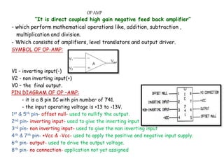
  • 1. OP AMP “It is direct coupled high gain negative feed back amplifier” - which perform mathematical operations like, addition, subtraction , multiplication and division. - Which consists of amplifiers, level translators and output driver. SYMBOL OF OP-AMP: V1 – inverting input(-) V2 - non inverting input(+) V0 – the final output. PIN DIAGRAM OF OP –AMP: - it is a 8 pin IC with pin number of 741. - the input operating voltage is +13 to -13V. 1st & 5th pin- offset null- used to nullify the output. 2nd pin- inverting input- used to give the inverting input 3rd pin- non inverting input- used to give the non inverting input 4th & 7th pin- +Vcc & -Vcc- used to apply the positive and negative input supply. 6th pin- output- used to drive the output voltage. 8th pin- no connection- application not yet assigned
  • 2. BLOCK DIAGRAM OF OP AMP: “ It is a four stage operational amplifier” Which consists of i) input stage- differential amplifier ii) intermediate stage- voltage amplifier iii) level shifting stage- level translator iv) output stage- output driver i) differential amplifier- which produce the two differential output with high input impedance ii) voltage amplifier- which produce the single ended amplified output iii) level translator- it is used to translate the dc level at the output downwards to zero iv) output driver- used to increases the output voltage swing and current supplying capability CHARACTERISTICS OF OP AMP: 1. high input impedance Ri=∞ 2. low output impedance R0= 0 3. high bandwidth BW= ∞ 4. perfect balance V0= 0
  • 3. Parameters of op-amp: 1)Input offset Voltage- it is the voltage that must be applied between the two input terminals of an op-amp to null the output. 2) Input offset current- The algebraic difference between the current in the inverting and non inverting terminal 3) Input Bias Current- it is the average current flows in the inverting and non- inverting terminal of an op amp. 4) Large Signal Voltage gain- It is the ratio of the output voltage and the differential input voltage[ Vo/Vid] 5) Output Voltage Swing- which indicates the values of positive and negative saturation voltage of the op-amp. For 741 IC, it is +13 and -13V. 6) Differential input resistance Ri- it is the equivalent resistance that can be measured at either the inverting or non-inverting input terminals with the other terminal connected to ground.(2Mohm). 7) Input Capacitance Ci- it is the equivalent capacitance that can be measured at either the inverting or non-inverting input terminal with the other terminal connected to ground.(1.4 pF). 8) Common Mode Rejection Ratio(CMRR)- It is defined as the ratio of the differential mode voltage gain (Ad) and common mode voltage gain. CMRR = Ad/Acm 9) Supply voltage Rejection Ratio- The change in an op-amps input offset voltage Vio caused by variations in the supply voltage is called the SVRR. SR= ΔVio/ΔV 10) Slew Rate- it is defined as the maximum rate of change of output voltage per unit of time and is expressed as volts per micro second.
  • 4. VIRTUAL GROUND “In op-amp, The non inverting terminal is connected to ground but the inverting terminal is not directly connected to ground. But it acts like a ground terminal. Therefore the inverting terminal is said to be at virtual ground” “the differential input voltage is ideally zero, that is the voltage at the inverting terminal V1 is approximately equal to that at the non inverting terminal V2.” ADVANTAGES OF OP-AMP i) Inexpensive ii) Versatile iii) Easy to use APPLICATIONS OF OP-AMP i) Used in negative amplifiers. ii) Used in wave shaping circuits iii) Used in filter circuit iv) Used in many mathematical operations. (a)inverting amplifier (b)non-inverting amplifier (c) summing amplifier (d) integrator (e) differentiator (f) Voltage follower. (g) Comparator (h) Zero crossing detector,etc
  • 5. INVERTING AMPLIFIER: “ It is an amplifier which shift phase of the input signal by 180 degree” - op amp 741 IC is used with power supply +Vcc & -Vcc. - the non inverting terminal is grounded. - the input voltage Vi is applied to inverting terminal through input resistance Ri. - the feedback resistance Rf is connected between Vs and Vo. - the output voltage measured from Vo. Applying Kirchhoff's current law, Vo= -Vi(Rf/Ri); Vo= -Vi.Av; hence voltage gain Av= Rf/Ri From the above equation, the input voltage is inverted at the output side has been proved.
  • 6. NON INVERTING AMPLIFIER: “ It is an amplifier which does not shift the phase of the input signal” - op amp 741 IC is used with power supply +Vcc & -Vcc. - the inverting terminal is grounded through input resistance Ri. - the input voltage Vi is applied to non inverting terminal. - the feedback resistance Rf is connected between Vs and Vo. - the output voltage measured from Vo. Applying Kirchhoff's current law, Vo= Vi.Av; hence voltage gain Av= (1+Rf/Ri ) From the above equation, the input voltage does not inverted at the output side has been proved.
  • 7. SUMMING AMPLIFIER: “ It is an amplifier which add all the input voltage with phase shift” ”it is also known as voltage adder” - op amp 741 IC is used with power supply +Vcc & -Vcc. - the non inverting terminal is grounded. - the input voltages V1,V2&V3 are applied to inverting terminal through input resistances R1,R2&R3. - the feedback resistance Rf is connected between Vs and Vo. - the output voltage measured from Vo.
  • 8. Applying Kirchhoff's current law, From the above equation, the input voltages are added inverted at the output side has been proved.
  • 9. VOLTAGE FOLLOWER: “ It is an amplifier which follows the input voltage with unity gain ” - op amp 741 IC is used with power supply +Vcc & -Vcc. - the input voltage Vi is applied to non inverting terminal. - the inverting terminal is connected with Vo directly. - the output voltage measured from Vo. From the non inverting amplifier, here, Rf & Ri = 0; Vo = (1+0)Vi Vo = (1)Vi Vo = Vi From the above equation, the output voltage follows the input voltage with unity gain has been proved.
  • 10. COMPARATOR: “ It is a comparator which is used to compare the two input voltages ” - op amp 741 IC is used with power supply +Vcc & -Vcc. - the input voltage Vi is applied to non inverting terminal. - the reference voltage Vr is applied to inverting terminal. - the output voltage measured from Vo. When applying the voltages Vi and Vr the comparator may produce three different outputs such as, i) if Vi>Vr; Vo=+sat; when the positive voltage is greater than negative voltage the output voltage goes to positive saturation. ii) if Vi<Vr; Vo=-sat; when the positive voltage is less than negative voltage the output voltage goes to negative saturation. i) if Vi=Vr; Vo=0; when the positive voltage is equal to negative voltage the output voltage goes to 0.
  • 11. ZERO CROSSING DETECTOR: “ It is an amplifier which change the output from one state to another state when the input voltage crosses zero” Which consists of three blocks, -comparator, differentiator and half wave rectifier. - op amp 741 IC is used with power supply +Vcc & -Vcc. - the input voltage Vi is applied to non inverting terminal. - the inverting terminal is grounded. - the output voltage from the comparator Vo1 is connected with RC network. - the output from differentiator Vo2 is connected with diode in forward bias. - the final output Vo is measured from the half wave rectifier. When applying the voltage Vi, -every time the input voltage crosses zero from positive side to negative side the output goes to –ve saturation. -similarly the input voltage crosses zero from negative side to positive side the output goes to +ve saturation. -the comparator will produce the square wave at the output side(Vo1). -the differentiator will produce the positive and negative pulses at the output side(Vo2). -the half wave rectifier will produce only the positive pulses at the output side(Vo).
  • 12. INTEGRATOR: “ It is an amplifier which is used to integrate the input voltage” - op amp 741 IC is used with power supply +Vcc & -Vcc. - the non inverting terminal is grounded. - the input voltage Vi is applied to inverting terminal through input resistance Ri. - the feedback capacitance Cf is connected between Vs and Vo. - the output voltage measured from Vo. - current through the capacitance Ic= C(dv/dt)
  • 13. Applying Kirchhoff's current law, From the above equation, the input voltage is integrated at the output side has been proved. When applying square wave as input signal the integrator will produce triangle wave at the output side.
  • 14. DIFFERENTIATOR: “ It is an amplifier which is used to differentiate the input voltage” - op amp 741 IC is used with power supply +Vcc & -Vcc. - the non inverting terminal is grounded. - the input voltage Vi is applied to inverting terminal through input capacitance Ci. - the feedback resistance Rf is connected between Vs and Vo. - the output voltage measured from Vo. - current through the capacitance Ic= C(dv/dt)
  • 15. Applying Kirchhoff's current law, From the above equation, the input voltage is differentiated at the output side has been proved. When applying triangular wave as input signal the integrator will produce square wave at the output side.
  • 16. TIMER “It is a monolithic timing device which produce constant and accurate time delays” -It is a 8 pin IC with no”555” -available in DIP & metal can packages Which consists of, -23 transistors, 2 diodes and 16 resistors. Operating modes: - Astable multivibrator - Monostable multivibrator Specifications: - operating voltage +5v to +18v. - high output current - high temperature stability - adjustable duty cycle PIN DETAILS: - 1st & 8th pins are used for power supply - 2nd pin is used to trigger the timer - 3rd pin is used to measure the output voltage - 4th pin is used to reset the timer - 5th pin is used to apply control voltage - 6th pin is used to measure the threshold voltage - 7th pin is used to discharge the timer
  • 17. BLOCK DIAGRAM OF 555: The timer consist of following blocks, - 2 comparators - a RS flipflop - a transistor - a resistive network Threshold comparator: - which compare threshold voltage and Control voltage (2/3Vcc) then produce 0 when threshold voltage is high and produce 1 when control voltage is high. Trigger comparator: - which compare trigger voltage and 1/3Vcc then produce 0 when 1/3Vcc is high and produce 1 when trigger voltage is high. RS FlipFlop: - it has two inputs (S-set & R-reset) and two outputs (Q & Q). - when S=1 & R=0 then the output Q=1 & Q=0 - when S=0 & R=1 then the output Q=0 & Q=1 - when S=0 & R=0 then the output will not change Transistor: - the transistor used to discharge the voltage based on the output of flipflop. Resistive network: - the resistors are used to derive the control voltages to the comparators.
  • 18. WORKING PRINCIPLE: 1. The internal resistors act as a voltage divider network, providing (2/3)Vcc at inverting terminal of the upper comparator and (1/3)Vcc at the non inverting terminal of the lower comparator. 2. Upper comparator has a threshold input and a control input . 3. Output of the upper comparator is applied to Reset (R) input of the flip- flop. 4. The lower comparator has a 1/3Vcc input and a trigger input. 5. Output of the lower comparator is applied to set (S) input of the flip- flop. 6. When 1/3Vcc exceeds trigger voltage the lower comparator output is 1 this will set the flipflop, hence the timer output is high. 7. The complementary output of the flip-flop will cutoff the transistor which allow the capacitor to charge. 8. When threshold voltage exceeds 2/3Vcc the upper comparator output is 1 this will reset the flipflop, hence the timer output goes to low. 9. The complementary output of the flip-flop will switch on the transistor which discharge the capacitor.
  • 19. Astable Mutivibrator “It has no stable states and continuously switches between the two states without application of any external trigger. “Astable multivibrator is also called as Free Running oscillator or square wave generator ” The Astable multivibrator consist of following blocks, - 2 comparators - a RS flipflop - a transistor - a resistive and capacitance network The circuit connections are as follows: -The pins 2 and 6 are connected to The capacitor and hence there is no need for an external Trigger pulse. It will self trigger and act as a free running multivibrator. -pin 8 is connected to supply voltage(VCC).
  • 20. - Pin 3 is the output terminal driven from flipflop output Q . - the threshold voltage is developed by the capacitor and it is connected with non inverting input of upper comparator. - The control voltage is driven from 2/3Vcc at pin 5 and it is connected to ground via a capacitor (usually 0.01μF). - Pin 4 is the external reset pin used to reset the timer. Hence when not in use, pin 4 is usually tied to VCC . Operation: 1. Initially, the power-on, 2/3Vcc is developed at the inverting input of upper comparator and 1/3Vcc is developed on non inverting input of lower comparator. 2. There is no voltage across the capacitors, hence the upper comparator output is 0 and lower comparator is output 1. 3. This will set the flipflop, hence the astable multivibrator output is 1. 4. The complementary output of the flip-flop will cutoff the transistor which allow the capacitor to charge. 5. When capacitor exceeds 2/3Vcc the upper comparator output goes to 1, but this will not change the multivibrator output. 6. When capacitor exceeds 1/3Vcc the lower comparator output goes to 0, 7. This will reset the flipflop, hence the astable multivibrator output goes to 0. 8. The complementary output of the flip-flop will turn on the transistor which discharge the capacitor. 9. This cycle has continues upto switch off the power supply. As a result the square wave is generated and it is indicated in the waveforms.
  • 21. Wave form: circuit diagram: Duty cycle: the duty cycle is defined as the ratio between on time and the total time. D = TON/ T Therefore, percentage Duty Cycle is given by %D = (TON / T) * 100 T= TON+TOFF TON=TC(charging time); TOFF=TD(discharging time) TC = 0.693 * (R1 + R2) C TD = 0.693 * R2C T = TON + TOFF = TC + TD T = 0.693 * (R1 + R2) C + 0.693 * R2C T = 0.693 * (R1 + 2R2) C f = 1 / T = 1 / 0.693 * (R1 + 2R2) C Hz
  • 22. Monostable Mutivibrator “It has a stable states and a quasi stable state” “Monostable multivibrator is also called as rectangular wave generator ” The Monostable multivibrator consist of following blocks, - 2 comparators - a RS flipflop - a transistor - an external trigger input - a resistive and capacitance network The circuit connections are as follows: -pin 8 is connected to supply voltage(VCC). -pin 2 is the external trigger input, Connected with inverting input of the lower comparator. The trigger input is actually held at high level +Vcc. When trigger applied it will reduced to 1/3Vcc. -Pin 3 is the output terminal driven from flipflop output Q .
  • 23. - the threshold voltage is developed by the capacitor and it is connected with non inverting input of upper comparator. - The control voltage driven from 2/3Vcc at pin 5 and it is connected to ground via a capacitor (usually 0.01μF). - the 1/3Vcc voltage is connected with non inverting input of lower comparator. - Pin 4 is the external reset pin used to reset the timer. Hence when not in use, pin 4 is usually tied to VCC . - the upper comparator output is connected with R input and lower comparator output is connected with RS input of the flipflop. Operation: 1. Initially, the power-on, 2/3Vcc is developed at the inverting input of upper comparator and 1/3Vcc is developed on non inverting input of lower comparator. 2. There is no voltage across the capacitors, hence the upper comparator output is 0 and lower comparator is output 1. 3. The output of the flipflop is 0, hence the monostable multivibrator output is also 0. 4. When applying the external negative trigger pulse, the inverting input voltahge goes below1/3Vcc,. 5. Then the output of flipflop is 1,hence the monostable multivibrator output is also 1. 6. The complementary output of the flip-flop will cutoff the transistor which allow the capacitor to charge. 7. The negative trigger pulse available for short period only again it will retain to +vcc level, hence the lower comparator output goes to 1 again. 8. When capacitor exceeds 2/3Vcc the upper comparator output goes to 1, this will reset the flipflop, hence the astable multivibrator output goes to 0. 9. The complementary output of the flip-flop will turn on the transistor which discharge the capacitor.
  • 24. 10.This cycle has continues upto switch off the power supply, so the monostable multivibrator produce output high when apllying the trigger pulse. 11. As a result the rectangle wave is generated and it is indicated in the waveforms. Wave form: circuit diagram: Duty cycle: the duty cycle is defined as the ratio between on time and the total time. D = TON/ T Therefore, percentage Duty Cycle is given by %D = (TON / T) * 100 T= TON+TOFF TON=TC(charging time); TOFF=TD(discharging time) TC = 0.693 * RC TD = 0.693 *C T = TON + TOFF = TC + TD T = 0.693 * R C + 0.693 *C T = 0.693 * (1+ R)C f = 1 / T = 1 / 0.693 * (1+R)C Hz
  • 25. Sequence Timer “It has four timers which are connected in cascade manner and switched on one by one” - all the four timers are operated at monostable mode. in monostable mode: - when applying trigger pulse the output goes to high level: quasi stable state - when capacitor exceed 2/3Vcc the output goes to low level: stable state - the quasi stable state is depends on the value of R&C. - differentiator circuit and diodes are used to indicate the timers output.
  • 26. Operation: - the first timer is switched On manually by closing the switch. - then the timer 1 will produce the output 1 which indicated by LED1. - after T1 second the first timer goes to 0 level, this will trigger the second timer. - then the timer 2 will produce the output 1 which indicated by LED2. - after T2 second the second timer goes to 0 level, this will trigger the third timer. - then the timer 3 will produce the output 1 which indicated by LED3. - after T3 second the third timer goes to 0 level, this will trigger the fourth timer. - then the timer 4 will produce the output 1 which indicated by LED4. - after T4 second the second timer goes to 0 level. The time T1=R1C1; T2=R2C2; T3=R3C3; T4=R4C4. Advantages: 1. timings are more reliable. 2. operates at low voltage. 3. occupies less space. 4. no need of warm up. Applications: 1. advertising boards. 2. shops displays and etc.
  • 27. Schmitt trigger “It is a converter which convert the varying input signal into square wave signal” - it is one type of multivibrator. - the sinusoidal input signal is applied to non inverting terminal of upper comparator and inverting terminal of lower comparator through R1 & R2.
  • 28. Operation: - at the initial level, no input voltage is applied the SRFF is set condition and the multivibrator output also in high. - when applying the input voltage, the input voltage exceeds 2/3vcc the upper comparator goes to high level. - at the same time the lower comparator produce the output low, hence the multivibrator output goes to low. - when the input voltage decreases less than 1/3Vcc the upper comparator goes to low level. - at the same time the lower comparator produce the output high, hence the multivibrator output goes to high. - when the input voltage between 1/3Vcc and 2/3Vcc the flipflop will not change the output state. - as a result the input signal was converted into square wave signal as shown below.
  • 29. PWM- pulse width modulation Modulation- it is a process of varying characteristics of carrier signal in accordance with message signal. pulse width modulation- - it is a process of varying the width of the carrier signal accordance with amplitude of message signal. - it is also called as pulse length modulation. - the monostable multivibrator is used as pulse width modulator. - the output period is varied according with amplitude of message signal. - trigger is applied for control the starting of pulses.
  • 30. Applications: 1. used in ramp generator 2. used in frequency divider 3. used in communication systems. Advantages: 1. increase the transmission range 2. reduce size of the antenna 3. increase efficiency 4. reduce noise.
  • 31.
  • 32. BOOLEAN ALGEBRA Number system: Decimal number system- the numbers from 0 to 9 are called as decimal number system with base of 10. Binary number system- the values 0 and 1 are called as binary number system with base of 2. Octal number system- the numbers from 0 to 7 are called as decimal number system with base of 8. Hexa Decimal number system- the numbers from 0 to 9 and A to F are called as decimal number system with base of 16. BCD- binary coded decimal- it is a decimal number represented in binary form by 0 and 1.
  • 33. Conversion from one number to other number system: Decimal to binary system: Binary to decimal system: Decimal to octal system: Decimal reminder Binary 2710 27÷2=13 1 13÷2=6 1 6÷2=3 0 3÷2=1 1 110112
  • 34. Binary to octal system: Decimal to hexa-decimal system: Hexa-decimal to decimal system:
  • 35. Octal to Binary system: Ex:326 Binary to octal system: Ex: 1101001 BCD to decimal: ex: 881 Hexa-decimal to binary system: Ex: A26 decimal to BCD: ex:100110000001 Binary to Hexa-decimal system: Ex: 1101101001
  • 36. Boolean algebra “it is a mathematical tool used to solve mathematical and logical operations” - It was invented by George boole in 1854. - 0 and 1 are the elements of boolean algebra. - Boolean operations: AND, OR, NOT, NAND, NOR and EXOR Basics Laws And Demorgan‟s Theorems Basic laws of Boolean Algebra 1. OR law A + 0 = A where A can be either 0 or 1. A + 1 = 1 where A can be either 0 or 1. A + Ā = 1 where A can be either 0 or 1. A + A = A where A can be either 0 or 1. 2. AND law A . 0 = 0 where A can be either 0 or 1. A . 1 = A where A can be either 0 or 1 A . A = A where A can be either 0 or 1. A . Ā = 0 where A can be either 0 or 1. 3. Laws of Complementation (A‘)‘=A 4. Commutative law A+B=B+A A.B=B.A
  • 37. 5. Associative law A+(B+C)=(A+B)+C A.(B.C)=(A.B).C 6. Distributive law A+(B.C)=(A+B)(A+C) A.(B+C)=A.B+A.C 7. Some of the following theorems are solved by the basic laws are 1.A+AB=A 2.A.(A+B)=A 3.A+A‘B=A+B 4.(A+B)(A+B‘)=A 5. AB+AB‘=A Demorgan‟s Theorems: i) First law: A +B = A . B Demorgan‘s first theorem states that the complement of a sum equals the product of the complements. ii) Second law: A . B = A + B Demorgan‘s second theorem states that the complement of a product equals the sum of thecomplement.
  • 38. i) First law: A +B = A . B - a OR gate, three NOT gate and one AND. gates are used i) Second law: A . B = A + B - a OR gate, three NOT gate and one AND. gates are used
  • 39. GATE “It is a logic device with one or more input and produce only one output” LOGIC GATES: -The most common logic gates are OR, AND, Not, NAND and NOR gates. -OR, AND ,NOT are called fundamental gates. -EX-OR gate is the combination of AND,OR, and NOT gates. UNIVERSAL GATES: -we can develop all other gates from a gate is called as universal gate. -NAND,NOR gates are called as universal gates. -it is also called as developed gates. OR GATE: LOGICAL ADDITION It is a addition gate with two inputs(A&B) and produce only one output(Y). Logical expression: Y=A+B Logical diagram: Truth table: Operation: - when A=0&B=0, both the switches are open the output Y=0 - when A=0&B=1, switch A is open and B is closed then the output Y=1 - when A=1&B=0, switch A is closed and B is open then the output Y=1 - when A=0&B=1, both the switches are closed the output Y=1
  • 40. AND GATE: LOGICAL MULTIPLICATION It is a product gate with two inputs(A&B) and produce only one output(Y). Logical expression: Y=A.B Logical diagram: Truth table: Operation: - when A=0&B=0, both the switches are open the output Y=0 - when A=0&B=1, switch A is open and B is closed then the output Y=0 - when A=1&B=0, switch A is closed and B is open then the output Y=0 - when A=0&B=1, both the switches are closed the output Y=1 NOT GATE: COMPLEMENT It is a complement gate with one input A and produce only one output Y. Logical expression: Y=A’ Logical diagram: Truth table: Operation: - when A=0, the switch is open the output Y=1 - when A=1, the switch is closed the output Y=0
  • 41. NOR GATE: COMPLEMENT OR It is a complement gate of OR gate with two inputs(A&B) and produce only one output(Y). Logical expression: Y=A+B Logical diagram: Truth table: Operation: - when A=0&B=0, both the switches are open the output Y=1 - when A=0&B=1, switch A is open and B is closed then the output Y=0 - when A=1&B=0, switch A is closed and B is open then the output Y=0 - when A=0&B=1, both the switches are closed the output Y=0 NAND GATE: COMPLEMENT AND It is a complement gate of AND gate with two inputs(A&B) and produce only one output(Y). Logical expression: Y=A.B Logical diagram: Truth table: Operation: - when A=0&B=0, both the switches are open the output Y=1 - when A=0&B=1, switch A is open and B is closed then the output Y=1 - when A=1&B=0, switch A is closed and B is open then the output Y=1 - when A=0&B=1, both the switches are closed the output Y=0
  • 42. EX-OR GATE: EXCLUSIVE OR GATE It is a combination of AND,OR and NOT gates with two inputs(A&B) and produce only one output(Y). Logical expression: Y=A B Logical diagram: Truth table: Operation: “when both the inputs are different the output is 1” - when A=0&B=0, both the switches are open the output Y=0 - when A=0&B=1, switch A is open and B is closed then the output Y=1 - when A=1&B=0, switch A is closed and B is open then the output Y=1 - when A=0&B=1, both the switches are closed the output Y=0 +
  • 43. Realization of gates using universal gate NAND: “NAND gate can be used to perform functions of any of the basic logic gates, then only it is called as universal gate” We can design the following gates using NAND gate: NOT, AND, OR, NOR, and EXOR NOT gate: -NOT gate is constructed using NAND gate by connecting two inputs together. output Y=A.A = A AND gate: -AND gate is constructed using two NAND gates by connecting together. output Y=A.B = A.B [A=A] OR gate: -OR gate is constructed using three NAND gates by connecting together. output Y=A.B = A+B = A+B [by Demorgans theorem A+B=A.B]
  • 44. Realization of gates using universal gate NOR: “NOR gate can be used to perform functions of any of the basic logic gates, then only it is called as universal gate” We can design the following gates using NOR gate: NOT, AND, OR, NOR, and EXOR NOT gate: -NOT gate is constructed using NOR gate by connecting two inputs together. output Y=A+A = A OR gate: -OR gate is constructed using two NOR gates by connecting together. output Y=A+B = AB [A=A] AND gate: -AND gate is constructed using three NOR gates by connecting together. output Y=A+B = A.B = A+B [by Demorgans theoremA+B =A.B ]
  • 45. Karnaugh map- k map “it is a simple method used to reduce the boolean expressions” - it is grouped by minterms. - types of k-map: - 2 variable, 3 variable and 4 variable k map. 2 variable: 3 variable: 4 variable:
  • 46. looping: combining the possible adjacent 1s in k map is called looping. Pairs: combining 2 adjacent 1s Quads: combining 4 adjacent 1s Octets: combining 8 adjacent 1s Rules: 1. Two adjacent cells have 1s, form pair. 2. Four adjacent cells have 1s, form Square.( QUADS) 3. Four corner cells have 1s, form square. .( QUADS) 4. Eight adjacent cells have 1s form OCTETS. 5. Two corner cells have 1s, form pair. 6. Otherwise takes single cell.