This document provides information about Xilinx Zynq UltraScale+ MPSoCs, including:
- An overview of the different device types - CG (commercial grade), EG (extended temperature), and EV (automotive) with their key components.
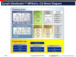
- Block diagrams and descriptions of the processing system and programmable logic for each device type.
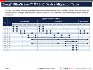
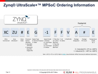
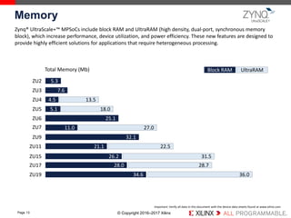
- Tables comparing the specifications of devices within each type such as logic resources, memory, connectivity, and integrated IP.
- Potential applications for each device type including image processing, video, networking, and more.