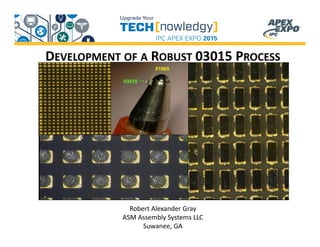


![Component Type Nomenclature
Component Nomenclature
[in ]x [in] English Metric [mm] x [mm]
0,010 in × 0,005 008004 0201** 0,25 x 0,125
0,012 in × 0,006 n.a. 03015* 0,3 x 0,15
0,016 in × 0,0079 01005 0402 0,4 x 0,2
0,024 in × 0,012 0201 0603 0,6 x 0,3
0,039 in × 0,020 0402 1005 1,0 x 0,5
0,063 in × 0,031 0603 1680 1,6 x 0,8
0,079 in × 0,049 0805 2012 2,0 x 1,25
0,098 in × 0,079 1008 2520 2,5 x 2,0
0,13 in × 0,063 1206 3216 3,2 x 1,6
0,13 in × 0,098 1210 3225 3,2 x 2,5
0,18 in × 0,063 1806 4516 4,5 x 1,6
0,18 in × 0,13 1812 4532 4,5 x 3,2
0,20 in × 0,098 2010 5025 5,0 x 2,5
0,25 in × 0,13 in 2512 6332 6,3 x 3,2
* ROHM, Panasonic
** Murata](https://image.slidesharecdn.com/544de205-12fa-4715-a4c0-1ef8a2166b64-150513163343-lva1-app6892/85/Robust-03015-process-RGray-apex15-5-320.jpg)


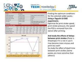


This document summarizes the development of a robust SMT process for placing 03015 components, which are only 0.3mm x 0.15mm in size. Through testing different solder pastes and stencil materials, the author developed a process using a laser-cut fine grain stainless steel stencil with an electro polish and nano coating that achieved over 80% transfer efficiency. Taguchi experiments were used to optimize print parameters. Initial tests achieved placement of 03015 components with 0 defects out of 36,000 placements. The printing process achieved a DPMO of 15. Further work is still needed to optimize the process for thinner stencils required by smartphones.


