A solar power generation system with a seven level inverterAsoka Technologies
This paper proposes a new solar power generation system, which is composed of a dc/dc power converter and a new seven-level inverter. The dc/dc power converter integrates a dc–dc boost converter and a transformer to convert the output voltage of the solar cell array into two independent voltage sources with multiple relationships. This new seven-level inverter is configured using a capacitor selection circuit and a full-bridge power converter, connected in cascade. The capacitor selection circuit converts the two output voltage sources of dc–dc power converter into a three-level dc voltage, and the full-bridge power converter further converts this three-level dc voltage into a seven-level ac voltage. In this way, the proposed solar power generation system generates a sinusoidal output current that is in phase with the utility voltage and is fed into the utility. The salient features of the proposed seven-level inverter are that only six power electronic switches are used, and only one power electronic switch is switched at high frequency at any time. A prototype is developed and tested to verify the performance of this proposed solar power generation system.
JPEEE1440 Cascaded Two-Level Inverter-Based Multilevel STATCOM for High-Pow...chennaijp
We offer different types of eee projects at affordable price in Chennai. You can easily choose titles with abstract and also full base paper for your reference.
For more details:
http://jpinfotech.org/final-year-ieee-projects/2014-ieee-projects/eee-projects/
The high penetration of power electronic based distributed energy resources (DERs) has increased the importance and attention given to voltage security of distribution systems. Voltage control in the electrical power system is critical for a proper operating condition. Therefore, distribution systems must have the ability to maintain a secure voltage profile. Using inverters for Volt/VAR control (VVC) can provide a faster response for voltage regulation than traditional voltage regulation devices, such as transformer load tap changers and voltage regulators. The primary objective of this paper is to demonstrate how smart inverters can be used to eliminate the voltage deviation by solving a mixed-integer quadratic program to determine the amount of reactive power that should be injected or absorbed at the appropriate nodes. The proposed method incorporates capacitor banks connected to the network and determines whether to turn on or off the capacitor bank for voltage regulation. These processes will be demonstrated in several cases that are focused on mitigating voltage-dips and swells.
The high penetration of power electronic based distributed energy resources (DERs) has increased the importance and attention given to voltage security of distribution systems. Voltage control in the electrical power system is critical for a proper operating condition. Therefore, distribution systems must have the ability to maintain a secure voltage profile. Using inverters for Volt/VAR control (VVC) can provide a faster response for voltage regulation than traditional voltage regulation devices, such as transformer load tap changers and voltage regulators. The primary objective of this paper is to demonstrate how smart inverters can be used to eliminate the voltage deviation by solving a mixed-integer quadratic program to determine the amount of reactive power that should be injected or absorbed at the appropriate nodes. The proposed method incorporates capacitor banks connected to the network and determines whether to turn on or off the capacitor bank for voltage regulation. These processes will be demonstrated in several cases that are focused on mitigating voltage-dips and swells.
Page 1 of 4 Direct Current (DC) Circuits Introduct.docxbunyansaturnina
Page 1 of 4
Direct Current (DC) Circuits
Introduction
In this lab, we will get acquainted with various components of electrical circuits. We will learn:
how to make simple circuits using a battery (or power supply), light bulbs, resistors; draw the
circuit diagram; how to use color code to read the resistance of the resistor; how to use the
measuring tools like a digital multimeter – DMM; how to connect the DMM to measure the
resistance, voltage and current. We will learn how to simplify the circuit by replacing the circuit
diagram with an equivalent one. Text reference: Young and Freedman §§ 26.1, 26.3.
We will investigate the behavior of direct current (DC) electrical circuits. We will study the flow
of electrical current in a circuit from the battery or power supply, through the wires, and through
various combinations of light bulbs and/or resistors.
A simple electrical circuit usually has a power (energy) source such as a battery or power supply
and resistors such as a light bulb or a carbon resistor. Here are the symbols for some electrical
components you may see in circuit diagrams of the lab manuals of this lab course:
A closed circuit is a path along which current carriers (electrons in conductors) can flow. Current
does not flow in an open circuit. A circuit in which there is a single pathway is known as a series
circuit whereas a circuit that has multiple (more than one) possible paths is known as a parallel
circuit.
Resistors impede the flow of current in a circuit. We assume that connecting leads (conductors)
have negligible resistance, while the insulators have very large resistance. Many resistors obey
Ohm’s Law (V = IR), which states that the current I through a resistance R is proportional to the
voltage V across the resistor. We will study Ohm’s law in the next lab class experiment.
Part 1. Light Bulbs
1. Simple circuit
Make a simple circuit using a battery or DC power supply, a light bulb (in its holder), and some of
the connecting leads.
a) What happens to the light bulb when you close the circuit?
___________________________________________________________________
b) Draw a circuit diagram representing your circuit using the symbols from above:
Try to remember how brightly the bulb is shining in step 1.
Page 2 of 4
2. Light bulbs in Series
Now add a second identical bulb in series (you will need to disconnect your circuit first).
a) Draw a proper diagram representing your circuit. What do you observe about the light
intensity (brightness) in each bulb compared to a single bulb in the previous step?
__________________________________________________________________
b) What happens if you remove one of the light bulbs from its holder?
_________________________________________________________________
3. Light bulbs in Parallel
Disconnect the circuit from step 2 and add the second bulb in parallel to the first.
a) Draw a proper diagram repres.
Sheet1resistance of resistorTime Constant = 5.3s10v from power sup.docxmaoanderton
Sheet1resistance of resistorTime Constant = 5.3s10v from power supply 54.37 kohmscapacitor 96.9 micro farradsY axistheoretical max 183.9 micro amps0835-0.7955515238536.610-1.61434389121016.215-2.4293808894157.8520-3.1538785998203.3925-3.9935622102251.8330-4.6100761648300.8635-5.3652150213350.4640-5.9909209211400.2545-6.6006864927450.18950-6.8804003955500.13355-7.2317982824550.10160-7.507026893860micro ampsseconds
5 10 15 20 25 30 35 40 45 50 55 60 -0.79555152381367755 -1.6143438912029549 -2.4293808893719371 -3.1538785998159584 -3.9935622102179167 -4.6100761647569461 -5.3652150213448593 -5.9909209211092715 -6.6006864927301665 -6.8804003955327699 -7.2317982823706588 -7.5070268937511528
Sheet285.5k ohms96.9 micro farrads10v from power supplyTime constant = 8.3Y axistheoretical max 117 micro amps050.18-0.8481529267823.616-1.60092722281611.324-2.3373712091244.8432-3.1852592141322.3440-3.9120230054401.1448-4.6311456724480.53456-5.3895333748560.31464-5.9205362279640.2172-6.3228216831720.14880-6.67271694800.12488-6.8496476482880.10896-6.987797986796micro ampsseconds
8 16 24 32 40 48 56 64 72 80 88 96 -0.84815292670693698 -1.6009272227661917 -2.3373712090794614 -3.185259214069216 -3.912023005428146 -4.6311456723913524 -5.3895333748196981 -5.92053622787164 -6.3228216830624246 -6.6727169400157784 -6.8496476481748561 -6.9877979866556732
Sheet384.37k ohms96.9 micro farradstime constant 5.310vx axisy axis4.855-0.66358837837.7410-1.48722027978.9815-2.28278246579.520-2.99573227369.7625-3.7297014486voltsseconds
5 10 15 20 25 -0.6635883783184009 -1.4872202797098513 -2.2827824656978661 -2.99573227355399 -3.7297014486341906
Sheet4resistance 85.5k ohm96.9 micro farradtime constant = 8.3s10vx axisy axis5.348-0.76356964497.8916-1.55589714559.0624-2.36446049679.5432-3.07911388259.7640-3.7297014486voltsseconds
8 16 24 32 40 seconds -0.76356964485649126 -1.5558971455060702 -2.3644604967121334 -3.0791138824930413 -3.7297014486341906
R-C Circuits
Purpose: This lab will consider another electrical component with unique characteristics, the capacitor. The lab will also provide practice constructing and interpreting graphs for the purpose of circuit analysis.
Introduction: As you have learned, a capacitor in its simplest form is two parallel plates of conductive material, separated by a non-conductive material that prevents the plates from touching. Capacitance, “C”, is measured in Farads (F), with typical values of capacitors being measured in μF. Capacitor labeling sometimes deviates from standard metric prefixes in that an upper case “M” is often used in place of the μ symbol for micro- (x 10-6). Do not confuse it with mega- (x 10+6). A mega-Farad capacitor would be enormous, if one could even be built!
As an electrical potential (voltage) is placed across the capacitor, electrical charge flows (current) from the voltage source and builds up on the plates of the capacitor. If connected to a DC source, the current will continue to fl.
Clamping Circuit and Clipping Circuit, Principle of Operation of Clamping Circuit, Biased positive clamping circuit, Biased negative clamping circuit, Classification of Clipping Circuit, Clipping Circuit, Zener Diode as a Peak Clipper, Application of Clipper.
,
International Refereed Journal of Engineering and Science (IRJES)irjes
International Refereed Journal of Engineering and Science (IRJES) is a leading international journal for publication of new ideas, the state of the art research results and fundamental advances in all aspects of Engineering and Science. IRJES is a open access, peer reviewed international journal with a primary objective to provide the academic community and industry for the submission of half of original research and applications.
1. 19/05/12 21:26Courseware – MITx 6.002x
Página 1 de 7https://6002x.mitx.mit.edu/courseware/6.002_Spring_2012/Week_10/Homework/
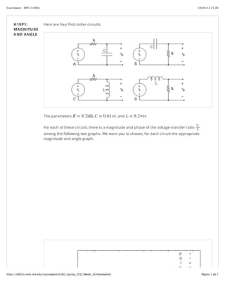
H10P1:
MAGNITUDE
AND ANGLE
Here are four first-order circuits:
The parameters k , nF, and mH.
For each of these circuits there is a magnitude and phase of the voltage-transfer ratio
among the following two graphs. We want you to choose, for each circuit the appropriate
magnitude and angle graph.
R = 8.2 Ω C = 0.61 L = 8.2
Vo
Vi
2. 19/05/12 21:26Courseware – MITx 6.002x
Página 2 de 7https://6002x.mitx.mit.edu/courseware/6.002_Spring_2012/Week_10/Homework/
3. 19/05/12 21:26Courseware – MITx 6.002x
Página 3 de 7https://6002x.mitx.mit.edu/courseware/6.002_Spring_2012/Week_10/Homework/
In the spaces provided please enter your choices. For example, if you chose magnitude and
angle for circuit A we want you to enter their product .
Circuit A:
Circuit B:
Circuit C:
Circuit D:
Check
p
u p ∗ u
H10P2:
IMPEDANCES
For each of the following circuits compute the impedance.
4. 19/05/12 21:26Courseware – MITx 6.002x
Página 4 de 7https://6002x.mitx.mit.edu/courseware/6.002_Spring_2012/Week_10/Homework/
In each space write an algebraic expression for the impedance in terms of , , , and . (As
usual, use for in your expressions.) In each case we also ask, "How does the impedance
behave as and as ?" If the answer is zero, enter a "0", if the answer is a constant
enter the algebraic expression for the constant, and if the answer is infinity, enter the symbol
"inf".
The impedance of circuit A,
As
As
The impedance of circuit B,
As
As
The impedance of circuit C,
As
Z R C L ω
w ω
ω → 0 ω → ∞
=ZA
ω → 0 →ZA
ω → ∞ →ZA
=ZB
ω → 0 →ZB
ω → ∞ →ZB
=ZC
ω → 0 →ZC
5. 19/05/12 21:26Courseware – MITx 6.002x
Página 5 de 7https://6002x.mitx.mit.edu/courseware/6.002_Spring_2012/Week_10/Homework/
As
The impedance of circuit D,
As
As
Check
ω → ∞ →ZC
=ZD
ω → 0 →ZD
ω → ∞ →ZD
H10P3:
AN L
NETWORK
The inductor and capacitor in the diagram below are part of the output-coupling network of a radio
transmitter. The rest of the transmitter (the source of radio-frequency energy) is represented as a
Thevenin source, and the antenna load is represented by a resistor.
In this problem we will examine some of the characteristics of this circuit. In the spaces provided
below you will write algebraic expressions in terms of the part parameters , , , , and the
angular frequency . (As usual, use for in your expressions.)
L C R1 R2
ω w ω
6. 19/05/12 21:26Courseware – MITx 6.002x
Página 6 de 7https://6002x.mitx.mit.edu/courseware/6.002_Spring_2012/Week_10/Homework/
One thing we want to know is the voltage-transfer ratio (the ratio of the complex amplitude of the
output voltage to the complex amplitude of the input voltage) of this network, as a function of the
operating frequency. Now that we know about impedances this is just like solving a resistive ladder!
In the space provided below write an algebraic expression for this ratio.
Look carefully at what you just computed. What is it for ? What happens as ? You
should always examine system functions this way.
Another important value is the driving-point impedance that the final amplifier "sees" looking at the
antenna through the coupling network. This is the ratio of the complex amplitude of the voltage
across the input port to the complex amplitude of the current into that port. In this circuit it is . In
the space provided below write an algebraic expression for this impedance. (Hint: The algebra is
often easier if you invert parallel impedances to make admittances. They then just add.)
Again, look carefully at what you just computed. What is it for ? What happens as ?
Remember that we found that in resistive circuits the load that absorbs the maximum power from a
Thevenin source is the one where the load resistance is the same as the source resistance. Here we
have an antenna that we want to transfer power to, but both the amplifier and the load have given
resistances and . Since capacitors and inductors do not eat power, they just store the energy
temporarily, perhaps if we choose the inductance and capcitance wisely we can couple the amplifier
to the antenna very well.
It is possible to find values of and that make the driving-point impedance you just computed
exactly , if . This will "match the antenna to the amplifier".
In the space provided below write an algebraic expression for the capacitance that allows this
match:
In the space provided below write an algebraic expression for the inductance that allows this
match:
Now let's look at some real numbers. For a big transmitting amplifier the output resistance may be
. A typical antenna has a radiation resistance of . Consider an AM
broadcast transmitter at kHz. In the spaces provided below, write the numerical values of
the capacitance (in picoFarads) and inductance (in microHenrys) for match.
Vo
Vi
ω = 0 ω → ∞
Vf
If
ω = 0 ω → ∞
R1 R2
L C
R1 >R1 R2
Cmatch
Lmatch
= 1000.0ΩR1 = 50.0ΩR2
f = 990.0
=Cmatch
7. 19/05/12 21:26Courseware – MITx 6.002x
Página 7 de 7https://6002x.mitx.mit.edu/courseware/6.002_Spring_2012/Week_10/Homework/
By the way, AM broadcast transmitters can be very large: up to 50kW. The parts used for such power
levels are impressive. For example, an inductor may be made of large gauge silver-coated copper
tubing. There is a nice picture here .
Check
=Lmatch