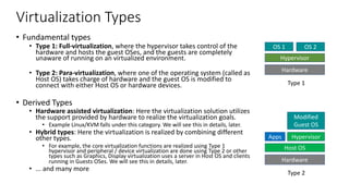
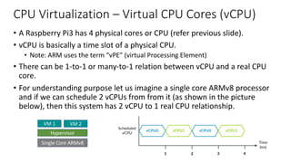
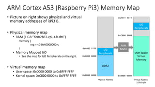
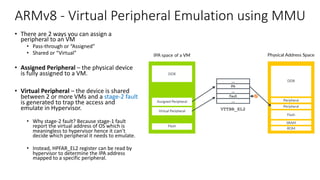
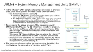
The document discusses virtualization in automotive ECUs, explaining its types and functions within the context of ARM's architecture, specifically the ARM Cortex-A53 processor. It describes full and para-virtualization, the role of hypervisors, and CPU virtualization aspects, including memory management and addressing. The document also covers how peripheral emulation and address translation are managed in virtualized environments, emphasizing the importance of hypervisor-controlled translations.

![ARM Cortex A53 – CPU core hardware blocks
• 4 CPU Cores with
• Timer block
• Interrupt block
• Core includes
• NEON Coprocessor
• FPU
• Crypto extensions
• L1 Cache [, L2 Cache]
• Debug & trace
• Trace block
• Debug block
• ACP - Accelerator Coherency
Ports for AXI slaves
• Master memory interface
• Power management interface
• Test interface
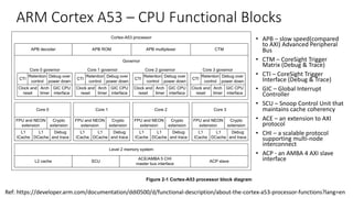
The Cortex-A53 processor is a mid-range, low-power processor that implements the ARMv8-A
architecture. The Cortex-A53 processor has one to four cores, each with an L1 memory system
and a single shared L2 cache.
Figure 1-1 shows an example of a Cortex-A53 MPCore configuration with four cores and either
an ACE or a CHI interface.
Figure 1-1 Example Cortex-A53 processor configuration
See About the Cortex-A53 processor functions on page 2-2 for more information about the
functional components.
Core 3*
Core 2*
Core 1*
AXI slave interface
Core 0
Timer events
Counter
ICDT*, nIRQ, nFIQ
PMU
ATB
Debug
Core
Trace
Debug
Interrupt
Timer
ACP*
Power
management
Test
ACE or CHI
master interface
Power control
DFT
MBIST
Cortex-A53 processor
* Optional
APB debug
Clocks
Resets
Configuration
Master
interface
ICCT*, nVCPUMNTIRQ
Ref: https://developer.arm.com/documentation/ddi0500/e/introduction/about-the-cortex-a53-processor](https://image.slidesharecdn.com/armv8-virtualizationsupport-v1-201024142956/85/Virtualization-Support-in-ARMv8-7-320.jpg)
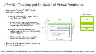
![ARMv8 – Switching to Hypervisor context
• ARM supports WFI instruction to put
the CPU in low power state.
• But, when HCR_EL2.TWI bit is set, if
either application or the OS executes
WFI instruction, then the CPU switches
to Hypervisor context.
• ARM also supports ‘HVC #[0-65535]’
instruction, which can be called from
OS context to switch the context to
Hypervisor.
• Note: ‘HVC #imm’ is undefined in
application context.
https://developer.arm.com/architectures/learn-the-architecture/armv8-a-virtualization/trapping-and-emulation-of-instructions
Copyright © 2019 Arm Limited (or its affiliates). All rights reserved.
Non-Confidential
Note: Traps are not just for virtualization. There are EL3 and EL1 controlled traps
traps are particularly useful to virtualization software. This guide only discusses th
typically associated with virtualization.
In our WFI example, an OS would usually execute a WFI as part of an idle loop. Wi
within a VM, the hypervisor can trap this operation and schedule a different vCPU
diagram shows:
5.1 Presenting virtual values of registers
Another example of using traps is to present virtual values of registers. For examp
ID_AA64MMFR0_EL1 reports support for memory system-related features in the](https://image.slidesharecdn.com/armv8-virtualizationsupport-v1-201024142956/85/Virtualization-Support-in-ARMv8-10-320.jpg)
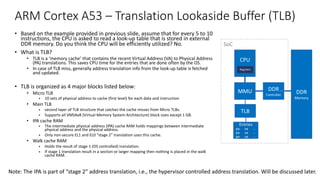
![ARM Cortex A53 – TLB matching and Cache handling
TLB match process
• Each TLB entry contains a VA, block-size, PA and a set of memory
properties (type, access permissions, ...)
• Each entry is associated with a particular ASID, contains a field to store
VMID
• A TLB entry match occurs, when the following conditions are met:
• Its VA, moderated by VA bits [47:N], where N is log2(page size) =
12 for 4k
• Memory space matches the memory space state of request. The
memory space can be one of four values:
• Secure EL3 (AArch64)
• Non-secure EL2
• Secure EL0, EL1 (and EL3 - AArch32)
• Non-secure EL0 or EL1
• ASID matches the current ASID held in the CONTEXTIDR, TTBR0
or TTBR1 or entry marked as global
• The VMID matches the current VMID held in the VTTBR register
Data cache coherency
• Uses MOESI protocol to maintain data coherency between
multiple cores.
• M - Modified - The line is in only this cache and is dirty (Unique Dirty)
• O - Owned - The line is possibly in more than one cache and is dirty
(Shared Dirty)
• E - Exclusive - The line is in only this cache and is clean. (Unique
Clean)
• S - Shared - The line is possibly in more than one cache and is clean
(Shared Clean)
• I - Invalid - The line is not in this cache
CPU
Registers
MMU
+ TLB
L1
Cache
L2
Cache
DDR
Memory
Virtual Address Physical Address
SoC
We will discuss
this soon
Key takeaway: Memory is already virtualized on a single OS, virtualizing it for more than one OS is done by adding stage-2 address translation.](https://image.slidesharecdn.com/armv8-virtualizationsupport-v1-201024142956/85/Virtualization-Support-in-ARMv8-16-320.jpg)
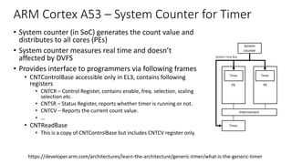
![ARM Cortex A53 – Generic Timer
Functional Description
• Each core has following set of 64bit timer:
• EL1 Non-secure physical timer
• EL1 Secure physical timer
• EL2 physical timer
• Virtual timer
• The system counter value (which resides in SoC) is
distributed to the Cortex-A53 processor via
CNTVALUEB[63:0]
• The system counter typically operate at lower frequency
than the CLKIN (main processor clock)
• Each timer provides an active-LOW interrupt output to the
SoC.
• External interrupt output pins (n = no-of-cores -1)
• nCNTPNSIRQ[n:0] - EL1 Non-secure physical timer event
• nCNTPSIRQ[n:0] - EL1 Secure physical timer event
• nCNTHPIRQ[n:0] - EL2 physical timer event
• nCNTVIRQ[n:0] - Virtual timer event
https://developer.arm.com/documentation/ddi0500/e/generic-timer/generic-timer-functional-description
frequency than the main processor CLKIN, the CNTCLKEN input is provided as a clock
enable for the CNTVALUEB bus. CNTCLKEN is registered inside the Cortex-A53 processor
before being used as a clock enable for the CNTVALUEB[63:0] registers. This allows a
multicycle path to be applied to the CNTVALUEB[63:0] bus. Figure 10-1 shows the interface.
Figure 10-1 Architectural counter interface
The value on the CNTVALUEB[63:0] bus is required to be stable whenever the internally
registered version of the CNTCLKEN clock enable is asserted. CNTCLKEN must be
synchronous and balanced with CLK and must toggle at integer ratios of the processor CLK.
See Clocks on page 2-9 for more information about CNTCLKEN.
Each timer provides an active-LOW interrupt output to the SoC.
Table 10-1 shows the signals that are the external interrupt output pins.
Cortex-A53 processor
Clock gate
CNTCLKEN
register
Architectural
counter
registers
CNTVALUEB[63:0]
CNTCLKEN
Table 10-1 Generic Timer signals
• Timer schedules events and trigger
interrupts based on an incrementing
counter value.
• It provides
• Generation of timer events as
interrupt outputs
• Generation of event streams](https://image.slidesharecdn.com/armv8-virtualizationsupport-v1-201024142956/85/Virtualization-Support-in-ARMv8-31-320.jpg)
![ARM Cortex A53 – Clocks and Resets
Clock Tree
• The Cortex-A53 processor has a single
clock input, CLKIN
• RPi3 uses 1.2GHz clock
• All cores in Cortex-A53 & SCU are
clocked with a distributed version of
CLKIN.
• Clock Tree
• PCLK - APB interface / bus
• ACLK - ACE (extension to AXI) bus, ACP
slave interface
• SCLK - SCU interface only if CHI protocol
is used.
• ATCLK - ATB interface, which can operate
at any integer multiple of main clock
• CNTCLK - 64-bit counter
Reset Inputs
• Cortex-A53 processor has the
following active-LOW reset input
signals
• nCPUPORESET[N:0] - primary, cold resets
signals initialize all resettable registers
• nCORERESET[N:0] - same as above,
except debug registers and ETM registers
• nPRESETDBG - single, cluster-wide signal
resets the integrated CoreSight
components that connect to the external
PCLK domain, such as debug logic
• nL2RESET - resets all resettable registers
in L2 memory system and the logic in the
SCU
• nMBISTRESET - an external MBIST
controller can use this signal to reset the
entire SoC.
Clock tree and resets are typically handled by Host OS. VMs generally don’t modify these.](https://image.slidesharecdn.com/armv8-virtualizationsupport-v1-201024142956/85/Virtualization-Support-in-ARMv8-34-320.jpg)

![Acronyms – 2 / 3
• DTS – Device Tree Structure
• DVFS – Dynamic Voltage and Frequency Scaling
• ECC – Error Correction Code
• ECU – Electronic Control Units in Cars
• ELx – Exception Level ‘x’ [x: 0 to 3 for ARMv8]
• ERET – Exception Return
• ESR – Exception Syndrome Register
• FIQ – Fast Interrupt Request (takes higher priority than IRQ)
• FPU – Floating Point Unit
• GIC – Global Interrupt Controller
• GICD - GIC Distributor
• GPU – Graphics Processing Unit
• HCR – Hypervisor Configuration Register
• HPFAR – Hyp IPA Fault Address Register. Holds the faulting IPA for some
aborts on stage 2 translation.
• HVC – Hypervisor Call
• I/O – Inputs and / or Outputs
• INTID – Interrupt Identifier
• IOMMU - I/O MMU, same as SMMU.
• IPA - Intermediate Physical Address
• IRQ – Interrupt Request (from I/O to CPU)
• ITS – Interrupt Translation Service that injects Interrupt directly to VMs.
• IVI – In-Vehicle Infotainment unit.
• KVM – Kernel-based Virtual Machine
• L1 – Level 1
• L2RESET – L2 Memory system reset
• LDR – Load from register
• log2 – Binary Logarithm
• LPI - Locality-specific Peripheral Interrupt are interrupts that uses ITS
• LR – Link Register
• MBIST – Memory Built In Self Test
• MBISTRESET – and external MBIST controller can reset the SoC
• MMU – Memory Management Unit
• NDA – Non Disclosure Agreement](https://image.slidesharecdn.com/armv8-virtualizationsupport-v1-201024142956/85/Virtualization-Support-in-ARMv8-43-320.jpg)
![Acronyms – 3 / 3
• OS – Operating Systems
• PA – Physical Address
• PC – Program Counter
• PCLK – Peripheral
• PE – Processing Element
• PMU – Performance Monitoring Unit
• PoC – Proof of Concept
• PPI - Private Peripheral Interrupt, targets single specific PE
• PRESETDBG - single, cluster-wide signal resets
• QNX – QNX Operating System
• RAM – Random Access Memory
• ROM – Read Only Memory
• SCLK – SCU Clock
• SCU – Snoop Control Unit that maintains cache coherency
• SGI – Software Generated Interrupts, generated by PEs.
• SMMU – System Memory Management Unit (the MMU for peripherals)
• SoC – System on Chip
• SPI – Shared Peripheral Interrupt
• SRAM – Static Random Access Memory
• STR - Store from Register
• TLB – Translation Lookaside Buffer
• TTBRx – Translation Table Base Register x [x: 0 or 1]
• UART – Universal Asynchronous Receive and Transmit. Serial Comms.
• VA – Virtual Address
• vCPU – Virtual CPU
• VM – Virtual Machine
• VMID – Virtual Machine Identifier
• VMSA – Virtual Memory System Architecture
• VTTBR – Virtualization Translation Table Base Register
• WFI – Wait For Interrupt](https://image.slidesharecdn.com/armv8-virtualizationsupport-v1-201024142956/85/Virtualization-Support-in-ARMv8-44-320.jpg)