Download to read offline


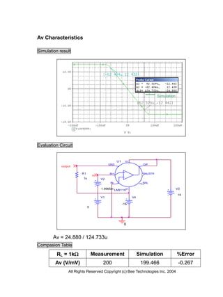


The document consists of a device modeling report for the LM311H voltage comparator, detailing its characteristics and simulation results. It includes various measurements and error percentages related to output voltage, response times, input offset voltage, and input bias current. Simulation evaluations indicate negligible errors in performance metrics, validating the model's accuracy.


