SlideShare a Scribd company logo
Page 1 of 23
MODEL NO :
MODEL VERSION: 00
SPEC VERSION : Ver 2.0
ISSUED DATE: 2016-04-01
■Preliminary Specification
□Final Product Specification
Customer :
Approved by Notes
Prepared by Checked by Approved by
W
h
a
t
s
a
p
p
:
 
8
6
 
1
8
5
6
6
2
9
4
2
1
8
S
k
y
p
e
:
 
p
a
n
o
x
s
h
a
w
n
@
o
u
t
l
o
o
k
.
c
o
m
E
m
a
i
l
:
 
s
h
a
w
n
.
l
e
e
@
p
a
n
o
x
d
i
s
p
l
a
y
.
c
o
m
P
a
n
o
x
 
D
i
s
p
l
a
y
 
P
r
o
v
i
d
e
 
L
C
D
/
O
L
E
D
Page 2 of 23
Table of Contents
Table of Contents .............................................................................................................................. 2
Record of Revision............................................................................................................................ 3
1 General Specifications ............................................................................................................... 4
2 Input/Output Terminals............................................................................................................... 5
2.1 LCD interface............................................................................................................................5
2.2 CTP interfcae............................................................................................................................6
3 Absolute Maximum Ratings ....................................................................................................... 7
4 Electrical Characteristics............................................................................................................ 7
4.1 LCD characteristics..................................................................................................................7
4.2 BL characteristics......................................................................................................................8
5 Timing Chart............................................................................................................................... 9
6 Optical Characteristics ............................................................................................................. 15
7 Environmental / Reliability Test ................................................................................................ 18
8 Mechanical Drawing................................................................................................................. 19
9 Packing Drawing ...................................................................................................................... 20
10 Precautions for Use of LCD Modules....................................................................................... 23
W
h
a
t
s
a
p
p
:
 
8
6
 
1
8
5
6
6
2
9
4
2
1
8
S
k
y
p
e
:
 
p
a
n
o
x
s
h
a
w
n
@
o
u
t
l
o
o
k
.
c
o
m
E
m
a
i
l
:
 
s
h
a
w
n
.
l
e
e
@
p
a
n
o
x
d
i
s
p
l
a
y
.
c
o
m
P
a
n
o
x
 
D
i
s
p
l
a
y
 
P
r
o
v
i
d
e
 
L
C
D
/
O
L
E
D
Page 3 of 23
Record of Revision
Rev Issued Date Description Editor
1.0 2015-12-29 Preliminary Specification Release Xunqiang Ji
2.0 2016-04-01
Modify Mechanical Drawing & Add Packing
Drawing
Xunqiang Ji
W
h
a
t
s
a
p
p
:
 
8
6
 
1
8
5
6
6
2
9
4
2
1
8
S
k
y
p
e
:
 
p
a
n
o
x
s
h
a
w
n
@
o
u
t
l
o
o
k
.
c
o
m
E
m
a
i
l
:
 
s
h
a
w
n
.
l
e
e
@
p
a
n
o
x
d
i
s
p
l
a
y
.
c
o
m
P
a
n
o
x
 
D
i
s
p
l
a
y
 
P
r
o
v
i
d
e
 
L
C
D
/
O
L
E
D
Page 4 of 23
1 General Specifications
Feature Spec
Display Spec.
Size 3.4 inch
Resolution 800(RGB) x 800
Technology Type a-Si
Pixel Configuration R.G.B. Vertical Stripe
Pixel pitch(um) 109.5*109.5
Display Mode SFT
Surface Treatment HC
Viewing Direction FREE
Mechanical
Characteristics
Module (W x H x D) (mm) with CTP 99.0 x 96.6 x 3.98
Active Area(mm) 87.6*87.6
With /Without TSP With CTP
Matching Connection Type FPC
LED Numbers 8 LEDs
CTP Surface hardness ≥7H
Weight (g) TBD
Electrical
Characteristics
Interface MIPI 3 lane
Color Depth 16.7M
LCD Driver IC ILI9881C
CTP Driver IC HX8526-E30
CTP Interface IIC
Note 1: Viewing direction for best image quality is different from TFT definition. There is a 180
degree shift.
Note 2: Requirements on Environmental Protection: Q/S0002
Note 3: LCM weight tolerance: ± 5%
W
h
a
t
s
a
p
p
:
 
8
6
 
1
8
5
6
6
2
9
4
2
1
8
S
k
y
p
e
:
 
p
a
n
o
x
s
h
a
w
n
@
o
u
t
l
o
o
k
.
c
o
m
E
m
a
i
l
:
 
s
h
a
w
n
.
l
e
e
@
p
a
n
o
x
d
i
s
p
l
a
y
.
c
o
m
P
a
n
o
x
 
D
i
s
p
l
a
y
 
P
r
o
v
i
d
e
 
L
C
D
/
O
L
E
D
Page 5 of 23
2 Input/Output Terminals
2.1 LCD Interface
Pin
No.
Symbol I/O Function Remark
1 GND GND Power Ground
2 LEDA P
LED Anode
3 LEDA P
4 LEDK P
LED Cathode
5 LEDK P
6 GND GND Power Ground
7 VDD(-5V) P
-5V INPUT
8 VDD(-5V) P
9 GND GND Power Ground
10 VDD(+5V) P
+5V INPUT
11 VDD(+5V) P
12 GND GND Power Ground
13 IOVCC P
Power supply 1.8V
14 IOVCC P
15 GND GND Power Ground
16 RESET I Global Reset Pin
17 GND GND Power Ground
18 TE I tearing effect output
19 GND GND Power Ground
20 NC N
No connect
21 NC N
22 NC N
23 GND GND Power Ground
24 LAN2_P I MIPI lane 2+
25 NC N No connect
26 LAN2_N I MIPI lane 2-
27 GND GND Power Ground
28 CLK_P I MIPI clock +
29 NC N No connect
W
h
a
t
s
a
p
p
:
 
8
6
 
1
8
5
6
6
2
9
4
2
1
8
S
k
y
p
e
:
 
p
a
n
o
x
s
h
a
w
n
@
o
u
t
l
o
o
k
.
c
o
m
E
m
a
i
l
:
 
s
h
a
w
n
.
l
e
e
@
p
a
n
o
x
d
i
s
p
l
a
y
.
c
o
m
P
a
n
o
x
 
D
i
s
p
l
a
y
 
P
r
o
v
i
d
e
 
L
C
D
/
O
L
E
D
Page 6 of 23
30 CLK_N I IMIPI clock -
31 GND GND Power Ground
32 LAN1_P I MIPI lane 1+
33 NC N No connect
34 LAN1_N I MIPI lane 1-
35 GND GND Power Ground
36 LAN0_P I MIPI lane 0+
37 NC N No connect
38 LAN0_N I MIPI lane 0-
39 GND GND Power Ground
2.2 CTP Interface
Pin Name
1 VCCA(2.8V)
2 VCCD(1.8V)
3 SCL
4 SDA
5 GND
6 GND
7 TSIX
8 NC
9 NC
10 XRES
W
h
a
t
s
a
p
p
:
 
8
6
 
1
8
5
6
6
2
9
4
2
1
8
S
k
y
p
e
:
 
p
a
n
o
x
s
h
a
w
n
@
o
u
t
l
o
o
k
.
c
o
m
E
m
a
i
l
:
 
s
h
a
w
n
.
l
e
e
@
p
a
n
o
x
d
i
s
p
l
a
y
.
c
o
m
P
a
n
o
x
 
D
i
s
p
l
a
y
 
P
r
o
v
i
d
e
 
L
C
D
/
O
L
E
D
Page 7 of 23
3 Absolute Maximum Ratings
GND=0V
Item Symbol MIN MAX Unit Remark
Power Supply Voltage IOVCC -0.3 3.3 V
Note1
Power Supply Voltage VDD(+5V) -0.3 6.5
Power Supply Voltage VDD(-5V) -6.5 0.3
Logic Supply Voltage VCCIO -0.3 3.3 V
Operating Temperature Top -20 70 ℃
Storage Temperature Tst -30 80 ℃
Relative Humidity
Note2
RH
-- ≤95 % Ta≤40℃
-- ≤85 % 40℃<Ta≤50℃
-- ≤55 % 50℃<Ta≤60℃
-- ≤36 % 60℃<Ta≤70℃
-- ≤24 % 70℃<Ta≤80℃
Absolute Humidity AH -- ≤70 g/m³ Ta>70℃
Table 3 Absolute Maximum Ratings
Note1: Input voltage include R0~R5, G0~G5, B0~B5, Dotclk, Hsync, Vsync, Enable, R/L, U/D.
4 Electrical Characteristics
4.1 LCD characteristics
GND=0V,Ta=25℃
Item Symbol MIN TYP MAX Unit Remark
Power Supply Voltage IOVCC 1.75 1.8 3.3 V
Power Supply Voltage VDD(+5V) 4.5 5.0 6 V
Power Supply Voltage VDD(-5V) -6 -5.0 -4.5
Input
Signal
Voltage
High Level VIH 0.7*IOVCC - IOVCC V
Low Level VIL 0 - 0.3*IOVCC V
Table 4.1 LCD module electrical characteristics
W
h
a
t
s
a
p
p
:
 
8
6
 
1
8
5
6
6
2
9
4
2
1
8
S
k
y
p
e
:
 
p
a
n
o
x
s
h
a
w
n
@
o
u
t
l
o
o
k
.
c
o
m
E
m
a
i
l
:
 
s
h
a
w
n
.
l
e
e
@
p
a
n
o
x
d
i
s
p
l
a
y
.
c
o
m
P
a
n
o
x
 
D
i
s
p
l
a
y
 
P
r
o
v
i
d
e
 
L
C
D
/
O
L
E
D
Page 8 of 23
4.2 Backlight Unit
Ta=25℃
Item Symbol Min Typ Max Unit Remark
Forward Current IF 18 20 22 mA 1 LED
Forward Voltage VF - 12.8 - V BLH-BLL
Backlight Power Consumption WBL - 512 - mW 8 LEDs
Operating Life Time - - 30,000 - Hrs For each LED
Note1: Figure below shows the connection of backlight LED.
Note 2: 1LED: VF =3.2V IF =20mA
Note 3: IF is defined for one LED.
Optical performance should be evaluated at Ta=25℃ only.
If LED is driven by high current, high ambient temperature & humidity condition. The life
time of LED will be reduced. Operating life means brightness goes down to 50% initial
brightness. Typical operating life time is estimated data.
LED CIRCUIT
LED K
LED A
(If=40mA / Vf=12.8V TYP)
W
h
a
t
s
a
p
p
:
 
8
6
 
1
8
5
6
6
2
9
4
2
1
8
S
k
y
p
e
:
 
p
a
n
o
x
s
h
a
w
n
@
o
u
t
l
o
o
k
.
c
o
m
E
m
a
i
l
:
 
s
h
a
w
n
.
l
e
e
@
p
a
n
o
x
d
i
s
p
l
a
y
.
c
o
m
P
a
n
o
x
 
D
i
s
p
l
a
y
 
P
r
o
v
i
d
e
 
L
C
D
/
O
L
E
D
Page 9 of 23
5 Timing Chart
5.1 MIPI Data to clock Timing Definition
5.1.1 High Speed Mode
W
h
a
t
s
a
p
p
:
 
8
6
 
1
8
5
6
6
2
9
4
2
1
8
S
k
y
p
e
:
 
p
a
n
o
x
s
h
a
w
n
@
o
u
t
l
o
o
k
.
c
o
m
E
m
a
i
l
:
 
s
h
a
w
n
.
l
e
e
@
p
a
n
o
x
d
i
s
p
l
a
y
.
c
o
m
P
a
n
o
x
 
D
i
s
p
l
a
y
 
P
r
o
v
i
d
e
 
L
C
D
/
O
L
E
D
Page 10 of 23
W
h
a
t
s
a
p
p
:
 
8
6
 
1
8
5
6
6
2
9
4
2
1
8
S
k
y
p
e
:
 
p
a
n
o
x
s
h
a
w
n
@
o
u
t
l
o
o
k
.
c
o
m
E
m
a
i
l
:
 
s
h
a
w
n
.
l
e
e
@
p
a
n
o
x
d
i
s
p
l
a
y
.
c
o
m
P
a
n
o
x
 
D
i
s
p
l
a
y
 
P
r
o
v
i
d
e
 
L
C
D
/
O
L
E
D
Page 11 of 23
5.1.2 Low Speed Mode
W
h
a
t
s
a
p
p
:
 
8
6
 
1
8
5
6
6
2
9
4
2
1
8
S
k
y
p
e
:
 
p
a
n
o
x
s
h
a
w
n
@
o
u
t
l
o
o
k
.
c
o
m
E
m
a
i
l
:
 
s
h
a
w
n
.
l
e
e
@
p
a
n
o
x
d
i
s
p
l
a
y
.
c
o
m
P
a
n
o
x
 
D
i
s
p
l
a
y
 
P
r
o
v
i
d
e
 
L
C
D
/
O
L
E
D
Page 12 of 23
W
h
a
t
s
a
p
p
:
 
8
6
 
1
8
5
6
6
2
9
4
2
1
8
S
k
y
p
e
:
 
p
a
n
o
x
s
h
a
w
n
@
o
u
t
l
o
o
k
.
c
o
m
E
m
a
i
l
:
 
s
h
a
w
n
.
l
e
e
@
p
a
n
o
x
d
i
s
p
l
a
y
.
c
o
m
P
a
n
o
x
 
D
i
s
p
l
a
y
 
P
r
o
v
i
d
e
 
L
C
D
/
O
L
E
D
Page 13 of 23
W
h
a
t
s
a
p
p
:
 
8
6
 
1
8
5
6
6
2
9
4
2
1
8
S
k
y
p
e
:
 
p
a
n
o
x
s
h
a
w
n
@
o
u
t
l
o
o
k
.
c
o
m
E
m
a
i
l
:
 
s
h
a
w
n
.
l
e
e
@
p
a
n
o
x
d
i
s
p
l
a
y
.
c
o
m
P
a
n
o
x
 
D
i
s
p
l
a
y
 
P
r
o
v
i
d
e
 
L
C
D
/
O
L
E
D
Page 14 of 23
5.2 Timing for DSI video mode
5.3 Reset Timing
W
h
a
t
s
a
p
p
:
 
8
6
 
1
8
5
6
6
2
9
4
2
1
8
S
k
y
p
e
:
 
p
a
n
o
x
s
h
a
w
n
@
o
u
t
l
o
o
k
.
c
o
m
E
m
a
i
l
:
 
s
h
a
w
n
.
l
e
e
@
p
a
n
o
x
d
i
s
p
l
a
y
.
c
o
m
P
a
n
o
x
 
D
i
s
p
l
a
y
 
P
r
o
v
i
d
e
 
L
C
D
/
O
L
E
D
Page 15 of 23
6 Optical Characteristics
6.1 Driving the backlight condition
Item Symbol Condition Min Typ Max Unit Remark
View Angles
θT
CR 10
≧
70 80 --
Degree Note2
θB 70 80 --
θL 70 80 --
θR 70 80 --
Contrast Ratio CR θ=0o
600 800 -- Note 3
Response Time
TON
25℃ -- 25 35 ms Note 4
TOFF
Chromaticity
White
x
Backlight is
on
0.263 0.313 0.363
Note 1,5
y 0.279 0.329 0.379
Red
x -- TBD --
Note 1,5
y -- TBD --
Green
x -- TBD --
Note 1,5
y -- TBD --
Blue
x -- TBD --
Note 1,5
y -- TBD --
Uniformity U 75 80 -- % Note 6
NTSC 65 70 -- % Note 5
Luminance L 280 350 -- cd/m2
Note 7
Test Conditions:
1. IF= 20 mA(one LED), and the ambient temperature is 25 .
℃
2. The test systems refer to Note 1 and Note 2.
W
h
a
t
s
a
p
p
:
 
8
6
 
1
8
5
6
6
2
9
4
2
1
8
S
k
y
p
e
:
 
p
a
n
o
x
s
h
a
w
n
@
o
u
t
l
o
o
k
.
c
o
m
E
m
a
i
l
:
 
s
h
a
w
n
.
l
e
e
@
p
a
n
o
x
d
i
s
p
l
a
y
.
c
o
m
P
a
n
o
x
 
D
i
s
p
l
a
y
 
P
r
o
v
i
d
e
 
L
C
D
/
O
L
E
D
Page 16 of 23
Note 1: Definition of optical measurement system.
The optical characteristics should be measured in dark room. After 5 Minutes operation, the optical
properties are measured at the center point of the LCD screen. All input terminals LCD panel must
be ground when measuring the center area of the panel.
Note 2: Definition of viewing angle range and measurement system.
viewing angle is measured at the center point of the LCD by CONOSCOPE(ergo-80)。
Note 3: Definition of contrast ratio
“White state “: The state is that the LCD should drive by Vwhite.
Item Photo detector Field
Contrast Ratio
SR-3A 1°
Luminance
Chromaticity
Lum Uniformity
Response Time BM-7A 2°
500mm
Photo detector
Field
LCD Panel
TFT-LCD Module
The center of the screen
W
h
a
t
s
a
p
p
:
 
8
6
 
1
8
5
6
6
2
9
4
2
1
8
S
k
y
p
e
:
 
p
a
n
o
x
s
h
a
w
n
@
o
u
t
l
o
o
k
.
c
o
m
E
m
a
i
l
:
 
s
h
a
w
n
.
l
e
e
@
p
a
n
o
x
d
i
s
p
l
a
y
.
c
o
m
P
a
n
o
x
 
D
i
s
p
l
a
y
 
P
r
o
v
i
d
e
 
L
C
D
/
O
L
E
D
Page 17 of 23
“Black state”: The state is that the LCD should drive by Vblack.
Vwhite: To be determined Vblack: To be determined.
Note 4: Definition of Response time
The response time is defined as the LCD optical switching time interval between “White” state and
“Black” state. Rise time (TON) is the time between photo detector output intensity changed from 90%
to 10%. And fall time (TOFF) is the time between photo detector output intensity changed from 10%
to 90%.
Note 5: Definition of color chromaticity (CIE1931)
Color coordinates measured at center point of LCD.
Note 6: Definition of Luminance Uniformity
Active area is divided into 9 measuring areas (Refer Fig. 2). Every measuring point is placed at the
center of each measuring area.
Luminance Uniformity (U) = Lmin/ Lmax
L-------Active area length W----- Active area width
Lmax: The measured Maximum luminance of all measurement position.
Lmin: The measured Minimum luminance of all measurement position.
Note 7: Definition of Luminance:
Measure the luminance of white state at center point.
W
h
a
t
s
a
p
p
:
 
8
6
 
1
8
5
6
6
2
9
4
2
1
8
S
k
y
p
e
:
 
p
a
n
o
x
s
h
a
w
n
@
o
u
t
l
o
o
k
.
c
o
m
E
m
a
i
l
:
 
s
h
a
w
n
.
l
e
e
@
p
a
n
o
x
d
i
s
p
l
a
y
.
c
o
m
P
a
n
o
x
 
D
i
s
p
l
a
y
 
P
r
o
v
i
d
e
 
L
C
D
/
O
L
E
D
Page 18 of 23
7 Environmental / Reliability Test
No Test Item Condition Remarks
1
High Temperature
Operation
Ts=+70℃, 120hrs
Restore 2H at 25℃
Power off
IEC60068-2-1:2007
GB2423.2-2008
2
Low Temperature
Operation
Ta=-20℃, 120hrs
Restore 2H at 25℃
Power off
IEC60068-2-1:2007
GB2423.1-2008
3
High Temperature
Storage
Ta=+80℃, 120hrs
Restore 2H at 25℃
Power off
IEC60068-2-1:2007
GB2423.2-2008
4
Low Temperature
Storage
Ta=-30℃, 120hrs
Restore 2H at 25℃
Power off
IEC60068-2-1:2007
GB2423.1-2008
5
Storage at High
Temperature and
Humidity
Ta=+60℃, 90% RH, 120 hours
Restore 2H at 25℃
Power off
IEC60068-2-78 :2001
GB/T2423.3—2006
7 ESD Sensitivity test
C=150pF, R=330Ω,5points/panel
Air:± 8KV, 5times,
Contact:± 4KV, 5 times,
(Environment: 15℃~35℃,
30%~60%, 86Kpa~106Kpa)
IEC61000-4-2:2001
GB/T17626.2-2006
Note1: Ts is the temperature of panel’s surface.
Note2: Ta is the ambient temperature of sample.
Note3: Before cosmetic and function test, the product must have enough recovery time, at least 2
hours at room temperature.
Note 4: In the standard condition, there shall be no practical problem that may affect the display
function. After the reliability test, the product only guarantees operation, but don’t guarantee all of the
cosmetic specification.
W
h
a
t
s
a
p
p
:
 
8
6
 
1
8
5
6
6
2
9
4
2
1
8
S
k
y
p
e
:
 
p
a
n
o
x
s
h
a
w
n
@
o
u
t
l
o
o
k
.
c
o
m
E
m
a
i
l
:
 
s
h
a
w
n
.
l
e
e
@
p
a
n
o
x
d
i
s
p
l
a
y
.
c
o
m
P
a
n
o
x
 
D
i
s
p
l
a
y
 
P
r
o
v
i
d
e
 
L
C
D
/
O
L
E
D
Page 19 of 23
8 Mechanical Drawing
2.25±0.15
2.10±0.15
1.10±0.15
1.00±0.15
0.30±0.15
0.30
+0.04
-0.03
0.10±0.03
0.60±0.07
10.80±0.05
R
0
.
2
0
0.30
+0.04
-0.03
0.60±0.03
0.30±0.03
0.30±0.07
11.40±0.05
12.00±0.1
0.1095
0.1095
Notes:
1.LCM
Display
Type:
A-Si
SFT;
CTP:
GFF
2.LCM
Drive
IC:
ILI9881C;
CTP
Drive
IC:
HX8526-E30
3.View
Direction:
ALL
4.LCM
Matched
Connector:
FH26W-39S-0.3SHW
CTP
Matched
Connector:
OK-22F010-04
5.General
Tolerance:
±0.2
6.Operation
Temp:
-20°~+70°C
Storage
Temp:
-30°~+80°C
7.Requirements
on
Environment
Protection:
Q/S0002
1.20
1.00
MAX(CTP)
99.00
47.30
1.00
MAX(LCM)
0.20±0.05
3.98±0.3
1.10±0.05(LENS)
1.35±0.1(CTP)
0.175(OCA)
0.50±0.1
34.70±0.5
?
96.60(LCM)
?
96.00(CTP
O.D)
?
92.00(
上台阶)
?
88.60(CTP
V.A)
?
87.60(LCD
A.A)
2.45(LCM)
32.40±0.5
(0.20)
2.60±0.3
4.00±0.5
12.42±0.5
2.50±0.3
YGT1-01
LCM+CTP
Chen
HuiXuan
Liu
Junwei
An
Guangkun
0
2016.03.30
Feng
SongLin
PIN
NAME
2
3
4
5
6
7
8
9
10
1
VCCA(2.8V)
VCCD(1.8V)
LCM
CTP
XRES
R
G
B
DOTS
DETAIL
Insulation
Tape
Component
Area
Bending
Area
No.
Symbol
2
3
4
5
6
7
8
9
10
11
12
13
14
15
16
17
18
19
20
21
22
23
24
1
25
26
27
28
29
30
GND
LEDA
LEDK
GND
NC
NC
GND
GND
GND
LAN2_N
VDD(-5V)
TE
VDD(+5V)
IOVCC(1.8V)
RESET
LAN2_P
CLK_P
CLK_N
GND
LAN1_P
LAN1_N
31
32
33
34
GND
LAN0_P
LAN0_N
GND
GND
35
36
37
38
39
GND
GND
GND
NC
NC
NC
NC
NC
IOVCC(1.8V)
VDD(+5V)
VDD(-5V)
LEDA
LEDK
NC
NC
TSIX
GND
GND
SDA
SCL
Printing
Black
800(RGB)X800
3.4"
TFT
Shield
SUS304
CTP
Connecter
SUS304
Shield
(If=40mA
/
Vf=12.8V
TYP)
PI
1
39
XXXXXXXXXXXX
(LCM)
1
39
A
A
K
XXXXXXXXXXXX
(BL)
(OK-22M010-04)
2016.03.30
2016.03.30
2016.03.30
1
.
0
0
W
h
a
t
s
a
p
p
:
 
8
6
 
1
8
5
6
6
2
9
4
2
1
8
S
k
y
p
e
:
 
p
a
n
o
x
s
h
a
w
n
@
o
u
t
l
o
o
k
.
c
o
m
E
m
a
i
l
:
 
s
h
a
w
n
.
l
e
e
@
p
a
n
o
x
d
i
s
p
l
a
y
.
c
o
m
P
a
n
o
x
 
D
i
s
p
l
a
y
 
P
r
o
v
i
d
e
 
L
C
D
/
O
L
E
D
Page 20 of 23
9 Packing Drawing
9.1 Per Carton
9.2 Packaging Specification and Quantity
W
h
a
t
s
a
p
p
:
 
8
6
 
1
8
5
6
6
2
9
4
2
1
8
S
k
y
p
e
:
 
p
a
n
o
x
s
h
a
w
n
@
o
u
t
l
o
o
k
.
c
o
m
E
m
a
i
l
:
 
s
h
a
w
n
.
l
e
e
@
p
a
n
o
x
d
i
s
p
l
a
y
.
c
o
m
P
a
n
o
x
 
D
i
s
p
l
a
y
 
P
r
o
v
i
d
e
 
L
C
D
/
O
L
E
D
Page 21 of 23
9.3 Packing Form
W
h
a
t
s
a
p
p
:
 
8
6
 
1
8
5
6
6
2
9
4
2
1
8
S
k
y
p
e
:
 
p
a
n
o
x
s
h
a
w
n
@
o
u
t
l
o
o
k
.
c
o
m
E
m
a
i
l
:
 
s
h
a
w
n
.
l
e
e
@
p
a
n
o
x
d
i
s
p
l
a
y
.
c
o
m
P
a
n
o
x
 
D
i
s
p
l
a
y
 
P
r
o
v
i
d
e
 
L
C
D
/
O
L
E
D
Page 22 of 23
9.4 Shipping Package of Palletizing Sequence
纸箱堆叠数按 2×3/每层×共 5 层 
W
h
a
t
s
a
p
p
:
 
8
6
 
1
8
5
6
6
2
9
4
2
1
8
S
k
y
p
e
:
 
p
a
n
o
x
s
h
a
w
n
@
o
u
t
l
o
o
k
.
c
o
m
E
m
a
i
l
:
 
s
h
a
w
n
.
l
e
e
@
p
a
n
o
x
d
i
s
p
l
a
y
.
c
o
m
P
a
n
o
x
 
D
i
s
p
l
a
y
 
P
r
o
v
i
d
e
 
L
C
D
/
O
L
E
D
Page 23 of 23
10 Precautions for Use of LCD Modules
10.1 Handling Precautions
10.1.1 The display panel is made of glass. Do not subject it to a mechanical shock by dropping
it from a high place, etc.
10.1.2 If the display panel is damaged and the liquid crystal substance inside it leaks out, be
sure not to get any in your mouth, if the substance comes into contact with your skin or clothes,
promptly wash it off using soap and water.
10.1.3 Do not apply excessive force to the display surface or the adjoining areas since this
may cause the color tone to vary.
10.1.4 The polarizer covering the display surface of the LCD module is soft and easily
scratched. Handle this polarizer carefully.
10.1.5 If the display surface is contaMinated, breathe on the surface and gently wipe it with a
soft dry cloth. If still not completely clear, moisten cloth with one of the following solvents:
- Isopropyl alcohol
- Ethyl alcohol
Solvents other than those mentioned above may damage the polarizer. Especially, do not use the
following:
- Water
- Ketone
- Aromatic solvents
10.1.6 Do not attempt to disassemble the LCD Module.
10.1.7 If the logic circuit power is off, do not apply the input signals.
10.1.8 To prevent destruction of the elements by static electricity, be careful to maintain an
optimum work environment.
10.1.8.1 Be sure to ground the body when handling the LCD Modules.
10.1.8.2 Tools required for assembly, such as soldering irons, must be properly ground.
10.1.8.3 To reduce the amount of static electricity generated, do not conduct assembly and
other work under dry conditions.
10.1.8.4 The LCD Module is coated with a film to protect the display surface. Be care when
peeling off this protective film since static electricity may be generated.
10.2 Storage precautions
10.2.1 When storing the LCD modules, avoid exposure to direct sunlight or to the light of
fluorescent lamps.
10.2.2 The LCD modules should be stored under the storage temperature range. If the LCD
modules will be stored for a long time, the recommend condition is:
Temperature : 0℃ ~ 40℃ Relatively humidity: ≤80%
10.2.3 The LCD modules should be stored in the room without acid, alkali and harmful gas.
10.3 Transportation Precautions
10.3.1 The LCD modules should be no falling and violent shocking during transportation, and
also should avoid excessive press, water, damp and sunshine.
W
h
a
t
s
a
p
p
:
 
8
6
 
1
8
5
6
6
2
9
4
2
1
8
S
k
y
p
e
:
 
p
a
n
o
x
s
h
a
w
n
@
o
u
t
l
o
o
k
.
c
o
m
E
m
a
i
l
:
 
s
h
a
w
n
.
l
e
e
@
p
a
n
o
x
d
i
s
p
l
a
y
.
c
o
m
P
a
n
o
x
 
D
i
s
p
l
a
y
 
P
r
o
v
i
d
e
 
L
C
D
/
O
L
E
D

More Related Content

What's hot

Smd philips-130419134912-phpapp02
Smd philips-130419134912-phpapp02Smd philips-130419134912-phpapp02
Smd philips-130419134912-phpapp02
Andy Jah
 
Lc1 d
Lc1 dLc1 d
Al5809
Al5809Al5809
Al5809
LeoCarrera5
 
VD-680-PS acf bondig machine user manual
VD-680-PS acf bondig machine user manualVD-680-PS acf bondig machine user manual
VD-680-PS acf bondig machine user manual
Vikas Deoarshi
 
Quanta bd1 r3b_schematics_da0wj1mb6f0
Quanta bd1 r3b_schematics_da0wj1mb6f0Quanta bd1 r3b_schematics_da0wj1mb6f0
Quanta bd1 r3b_schematics_da0wj1mb6f0
DATACORP
 
Sua chua may lanh cua daikin
Sua chua may lanh cua daikinSua chua may lanh cua daikin
Sua chua may lanh cua daikin
suadiennuochanoi.vn
 
MOSFETモデルにおけるLTspiceとPSpiceの比較
MOSFETモデルにおけるLTspiceとPSpiceの比較MOSFETモデルにおけるLTspiceとPSpiceの比較
MOSFETモデルにおけるLTspiceとPSpiceの比較
Tsuyoshi Horigome
 
Original IGBT N-Channel FGA25N120 25N120 ANTD 25A 1200V New
Original IGBT N-Channel FGA25N120 25N120 ANTD 25A 1200V NewOriginal IGBT N-Channel FGA25N120 25N120 ANTD 25A 1200V New
Original IGBT N-Channel FGA25N120 25N120 ANTD 25A 1200V New
authelectroniccom
 
Original IGBT FGA20S120M FGA20S 20S120 20A 1200V TO-3P New
Original IGBT FGA20S120M FGA20S 20S120 20A 1200V TO-3P NewOriginal IGBT FGA20S120M FGA20S 20S120 20A 1200V TO-3P New
Original IGBT FGA20S120M FGA20S 20S120 20A 1200V TO-3P New
authelectroniccom
 
Mrf1535 t1
Mrf1535 t1Mrf1535 t1
Mrf1535 t1
Jose Castañeda
 
Original IGBT FGPF50N33 50N33 50A 330V TO-220F New Fairchild
Original IGBT FGPF50N33 50N33 50A 330V TO-220F New FairchildOriginal IGBT FGPF50N33 50N33 50A 330V TO-220F New Fairchild
Original IGBT FGPF50N33 50N33 50A 330V TO-220F New Fairchild
AUTHELECTRONIC
 
Contactor LC1D schneider
Contactor LC1D schneiderContactor LC1D schneider
Contactor LC1D schneider
Hoàng Phương JSC
 

What's hot (18)

Diodo
DiodoDiodo
Diodo
 
Smd philips-130419134912-phpapp02
Smd philips-130419134912-phpapp02Smd philips-130419134912-phpapp02
Smd philips-130419134912-phpapp02
 
Lc1 d
Lc1 dLc1 d
Lc1 d
 
Al5809
Al5809Al5809
Al5809
 
Ds1307 datasheet
Ds1307 datasheetDs1307 datasheet
Ds1307 datasheet
 
VD-680-PS acf bondig machine user manual
VD-680-PS acf bondig machine user manualVD-680-PS acf bondig machine user manual
VD-680-PS acf bondig machine user manual
 
Ci
CiCi
Ci
 
Quanta bd1 r3b_schematics_da0wj1mb6f0
Quanta bd1 r3b_schematics_da0wj1mb6f0Quanta bd1 r3b_schematics_da0wj1mb6f0
Quanta bd1 r3b_schematics_da0wj1mb6f0
 
Sua chua may lanh cua daikin
Sua chua may lanh cua daikinSua chua may lanh cua daikin
Sua chua may lanh cua daikin
 
MOSFETモデルにおけるLTspiceとPSpiceの比較
MOSFETモデルにおけるLTspiceとPSpiceの比較MOSFETモデルにおけるLTspiceとPSpiceの比較
MOSFETモデルにおけるLTspiceとPSpiceの比較
 
Original IGBT N-Channel FGA25N120 25N120 ANTD 25A 1200V New
Original IGBT N-Channel FGA25N120 25N120 ANTD 25A 1200V NewOriginal IGBT N-Channel FGA25N120 25N120 ANTD 25A 1200V New
Original IGBT N-Channel FGA25N120 25N120 ANTD 25A 1200V New
 
Original IGBT FGA20S120M FGA20S 20S120 20A 1200V TO-3P New
Original IGBT FGA20S120M FGA20S 20S120 20A 1200V TO-3P NewOriginal IGBT FGA20S120M FGA20S 20S120 20A 1200V TO-3P New
Original IGBT FGA20S120M FGA20S 20S120 20A 1200V TO-3P New
 
74ls74 d
74ls74 d74ls74 d
74ls74 d
 
Mrf1535 t1
Mrf1535 t1Mrf1535 t1
Mrf1535 t1
 
Original IGBT FGPF50N33 50N33 50A 330V TO-220F New Fairchild
Original IGBT FGPF50N33 50N33 50A 330V TO-220F New FairchildOriginal IGBT FGPF50N33 50N33 50A 330V TO-220F New Fairchild
Original IGBT FGPF50N33 50N33 50A 330V TO-220F New Fairchild
 
74164
7416474164
74164
 
Tl 2844 b
Tl 2844 bTl 2844 b
Tl 2844 b
 
Contactor LC1D schneider
Contactor LC1D schneiderContactor LC1D schneider
Contactor LC1D schneider
 

Similar to Circle 3.4 Inch Round LCD Display 800*800 Screen With Mipi Controller Board For Smart Watch

8 inch TFT-LCD Datesheet, AUO, 800*1280, MIPI Interface
8 inch TFT-LCD Datesheet, AUO, 800*1280, MIPI Interface8 inch TFT-LCD Datesheet, AUO, 800*1280, MIPI Interface
8 inch TFT-LCD Datesheet, AUO, 800*1280, MIPI Interface
Panox Display
 
74 hc hct393
74 hc hct39374 hc hct393
74 hc hct393
kiennguyen1991
 
74hc73 ci-flip-flop-jk-datasheet
74hc73 ci-flip-flop-jk-datasheet74hc73 ci-flip-flop-jk-datasheet
74hc73 ci-flip-flop-jk-datasheet
Daniel Fiuza
 
74HC123.PDF
74HC123.PDF74HC123.PDF
74HC123.PDF
Edgar Rios
 
5.5 inch Amoled (1080x1920) Datasheet
5.5 inch Amoled (1080x1920) Datasheet5.5 inch Amoled (1080x1920) Datasheet
5.5 inch Amoled (1080x1920) Datasheet
Panox Display
 
3.81 inch OLED 1080X1200 MIPI
3.81 inch OLED 1080X1200 MIPI3.81 inch OLED 1080X1200 MIPI
3.81 inch OLED 1080X1200 MIPI
Panox Display
 
CMEL 2.4 inch Amoled(240x320) Datasheet
CMEL 2.4 inch Amoled(240x320) DatasheetCMEL 2.4 inch Amoled(240x320) Datasheet
CMEL 2.4 inch Amoled(240x320) Datasheet
Panox Display
 
TFT индикатор диагональю 4,3 дюйма WF43STVAEDNN0#
TFT индикатор диагональю 4,3 дюйма WF43STVAEDNN0#TFT индикатор диагональю 4,3 дюйма WF43STVAEDNN0#
TFT индикатор диагональю 4,3 дюйма WF43STVAEDNN0#
SEA Company
 
OLED Display 1.2 inch 60 Hz 390x390 QSPI
OLED Display 1.2 inch 60 Hz 390x390 QSPIOLED Display 1.2 inch 60 Hz 390x390 QSPI
OLED Display 1.2 inch 60 Hz 390x390 QSPI
Panox Display
 
3.81 inch Amoled(1080x1200) VR Datasheet
3.81 inch Amoled(1080x1200) VR Datasheet3.81 inch Amoled(1080x1200) VR Datasheet
3.81 inch Amoled(1080x1200) VR Datasheet
Panox Display
 
Original IC MIP0040MSSCF MIP004 004 DIP-7 New
Original IC MIP0040MSSCF MIP004 004 DIP-7 NewOriginal IC MIP0040MSSCF MIP004 004 DIP-7 New
Original IC MIP0040MSSCF MIP004 004 DIP-7 New
AUTHELECTRONIC
 
2.8 Inch LCD 320X240 C0283QGL-SPIRGB To Replace CMEL 2.8 C0283QGLC
2.8 Inch LCD 320X240 C0283QGL-SPIRGB To Replace CMEL 2.8 C0283QGLC2.8 Inch LCD 320X240 C0283QGL-SPIRGB To Replace CMEL 2.8 C0283QGLC
2.8 Inch LCD 320X240 C0283QGL-SPIRGB To Replace CMEL 2.8 C0283QGLC
Shawn Lee
 
1.63 inch OLED 320X320 MIPI Square OLED
1.63 inch OLED 320X320 MIPI Square OLED1.63 inch OLED 320X320 MIPI Square OLED
1.63 inch OLED 320X320 MIPI Square OLED
Panox Display
 
1.45 inch Amoled(280x280) Datasheet
1.45 inch Amoled(280x280) Datasheet1.45 inch Amoled(280x280) Datasheet
1.45 inch Amoled(280x280) Datasheet
Panox Display
 
0.47 inch LCD Micro Dispalay 800x600 Resolution RGB Interface LCD Screen
0.47 inch LCD Micro Dispalay 800x600 Resolution RGB Interface LCD Screen0.47 inch LCD Micro Dispalay 800x600 Resolution RGB Interface LCD Screen
0.47 inch LCD Micro Dispalay 800x600 Resolution RGB Interface LCD Screen
Shawn Lee
 
1.28 Inch Screen 240x240 Round LCD Display For Smart Watch Wearable Device
1.28 Inch Screen 240x240 Round LCD Display For Smart Watch Wearable Device1.28 Inch Screen 240x240 Round LCD Display For Smart Watch Wearable Device
1.28 Inch Screen 240x240 Round LCD Display For Smart Watch Wearable Device
Shawn Lee
 
VLSID 2015 FirmLeak (Poster)
VLSID 2015 FirmLeak (Poster)VLSID 2015 FirmLeak (Poster)
VLSID 2015 FirmLeak (Poster)
Anand Haridass
 
PANEL LCD lc320w01
PANEL LCD  lc320w01PANEL LCD  lc320w01
PANEL LCD lc320w01
mobarmej
 
Modulador de Ancho de Pulso en Fuentes ATX Sdc7500
Modulador de Ancho de Pulso en Fuentes ATX Sdc7500Modulador de Ancho de Pulso en Fuentes ATX Sdc7500
Modulador de Ancho de Pulso en Fuentes ATX Sdc7500
Juan Carlos Ruiz
 

Similar to Circle 3.4 Inch Round LCD Display 800*800 Screen With Mipi Controller Board For Smart Watch (20)

8 inch TFT-LCD Datesheet, AUO, 800*1280, MIPI Interface
8 inch TFT-LCD Datesheet, AUO, 800*1280, MIPI Interface8 inch TFT-LCD Datesheet, AUO, 800*1280, MIPI Interface
8 inch TFT-LCD Datesheet, AUO, 800*1280, MIPI Interface
 
74 hc hct393
74 hc hct39374 hc hct393
74 hc hct393
 
74hc73 ci-flip-flop-jk-datasheet
74hc73 ci-flip-flop-jk-datasheet74hc73 ci-flip-flop-jk-datasheet
74hc73 ci-flip-flop-jk-datasheet
 
74HC123.PDF
74HC123.PDF74HC123.PDF
74HC123.PDF
 
5.5 inch Amoled (1080x1920) Datasheet
5.5 inch Amoled (1080x1920) Datasheet5.5 inch Amoled (1080x1920) Datasheet
5.5 inch Amoled (1080x1920) Datasheet
 
3.81 inch OLED 1080X1200 MIPI
3.81 inch OLED 1080X1200 MIPI3.81 inch OLED 1080X1200 MIPI
3.81 inch OLED 1080X1200 MIPI
 
CMEL 2.4 inch Amoled(240x320) Datasheet
CMEL 2.4 inch Amoled(240x320) DatasheetCMEL 2.4 inch Amoled(240x320) Datasheet
CMEL 2.4 inch Amoled(240x320) Datasheet
 
TFT индикатор диагональю 4,3 дюйма WF43STVAEDNN0#
TFT индикатор диагональю 4,3 дюйма WF43STVAEDNN0#TFT индикатор диагональю 4,3 дюйма WF43STVAEDNN0#
TFT индикатор диагональю 4,3 дюйма WF43STVAEDNN0#
 
OLED Display 1.2 inch 60 Hz 390x390 QSPI
OLED Display 1.2 inch 60 Hz 390x390 QSPIOLED Display 1.2 inch 60 Hz 390x390 QSPI
OLED Display 1.2 inch 60 Hz 390x390 QSPI
 
3.81 inch Amoled(1080x1200) VR Datasheet
3.81 inch Amoled(1080x1200) VR Datasheet3.81 inch Amoled(1080x1200) VR Datasheet
3.81 inch Amoled(1080x1200) VR Datasheet
 
Original IC MIP0040MSSCF MIP004 004 DIP-7 New
Original IC MIP0040MSSCF MIP004 004 DIP-7 NewOriginal IC MIP0040MSSCF MIP004 004 DIP-7 New
Original IC MIP0040MSSCF MIP004 004 DIP-7 New
 
2.8 Inch LCD 320X240 C0283QGL-SPIRGB To Replace CMEL 2.8 C0283QGLC
2.8 Inch LCD 320X240 C0283QGL-SPIRGB To Replace CMEL 2.8 C0283QGLC2.8 Inch LCD 320X240 C0283QGL-SPIRGB To Replace CMEL 2.8 C0283QGLC
2.8 Inch LCD 320X240 C0283QGL-SPIRGB To Replace CMEL 2.8 C0283QGLC
 
1.63 inch OLED 320X320 MIPI Square OLED
1.63 inch OLED 320X320 MIPI Square OLED1.63 inch OLED 320X320 MIPI Square OLED
1.63 inch OLED 320X320 MIPI Square OLED
 
A
AA
A
 
1.45 inch Amoled(280x280) Datasheet
1.45 inch Amoled(280x280) Datasheet1.45 inch Amoled(280x280) Datasheet
1.45 inch Amoled(280x280) Datasheet
 
0.47 inch LCD Micro Dispalay 800x600 Resolution RGB Interface LCD Screen
0.47 inch LCD Micro Dispalay 800x600 Resolution RGB Interface LCD Screen0.47 inch LCD Micro Dispalay 800x600 Resolution RGB Interface LCD Screen
0.47 inch LCD Micro Dispalay 800x600 Resolution RGB Interface LCD Screen
 
1.28 Inch Screen 240x240 Round LCD Display For Smart Watch Wearable Device
1.28 Inch Screen 240x240 Round LCD Display For Smart Watch Wearable Device1.28 Inch Screen 240x240 Round LCD Display For Smart Watch Wearable Device
1.28 Inch Screen 240x240 Round LCD Display For Smart Watch Wearable Device
 
VLSID 2015 FirmLeak (Poster)
VLSID 2015 FirmLeak (Poster)VLSID 2015 FirmLeak (Poster)
VLSID 2015 FirmLeak (Poster)
 
PANEL LCD lc320w01
PANEL LCD  lc320w01PANEL LCD  lc320w01
PANEL LCD lc320w01
 
Modulador de Ancho de Pulso en Fuentes ATX Sdc7500
Modulador de Ancho de Pulso en Fuentes ATX Sdc7500Modulador de Ancho de Pulso en Fuentes ATX Sdc7500
Modulador de Ancho de Pulso en Fuentes ATX Sdc7500
 

More from Shawn Lee

Wearable 1.78 inch Square AMOLED Display 368*448 For Smart Watch Bracelet Scr...
Wearable 1.78 inch Square AMOLED Display 368*448 For Smart Watch Bracelet Scr...Wearable 1.78 inch Square AMOLED Display 368*448 For Smart Watch Bracelet Scr...
Wearable 1.78 inch Square AMOLED Display 368*448 For Smart Watch Bracelet Scr...
Shawn Lee
 
2.2 inch LCD Transflective TFT module 320*320 LH220Q32-FD01 Diastimeter Games...
2.2 inch LCD Transflective TFT module 320*320 LH220Q32-FD01 Diastimeter Games...2.2 inch LCD Transflective TFT module 320*320 LH220Q32-FD01 Diastimeter Games...
2.2 inch LCD Transflective TFT module 320*320 LH220Q32-FD01 Diastimeter Games...
Shawn Lee
 
1.91 Inch OLED Display Module Resolution 240*536 MIPI Interface for Wearable ...
1.91 Inch OLED Display Module Resolution 240*536 MIPI Interface for Wearable ...1.91 Inch OLED Display Module Resolution 240*536 MIPI Interface for Wearable ...
1.91 Inch OLED Display Module Resolution 240*536 MIPI Interface for Wearable ...
Shawn Lee
 
Flexible 1.36 inch 16*128 SPI SSD1316 Monochrome OLED Screen Module Panel
Flexible 1.36 inch 16*128 SPI SSD1316 Monochrome OLED Screen Module PanelFlexible 1.36 inch 16*128 SPI SSD1316 Monochrome OLED Screen Module Panel
Flexible 1.36 inch 16*128 SPI SSD1316 Monochrome OLED Screen Module Panel
Shawn Lee
 
1.5 Inch Flexible OLED Display 120x240 MIPI AMOLED Screen For Wearable Smart ...
1.5 Inch Flexible OLED Display 120x240 MIPI AMOLED Screen For Wearable Smart ...1.5 Inch Flexible OLED Display 120x240 MIPI AMOLED Screen For Wearable Smart ...
1.5 Inch Flexible OLED Display 120x240 MIPI AMOLED Screen For Wearable Smart ...
Shawn Lee
 
Wearable 1.78 inch Square AMOLED Display 368*448 For Smart Watch Bracelet Scr...
Wearable 1.78 inch Square AMOLED Display 368*448 For Smart Watch Bracelet Scr...Wearable 1.78 inch Square AMOLED Display 368*448 For Smart Watch Bracelet Scr...
Wearable 1.78 inch Square AMOLED Display 368*448 For Smart Watch Bracelet Scr...
Shawn Lee
 
Sony 0.71 inch AMOLED 1920x1080 OLED Display HD-MI Board Available USB Driver...
Sony 0.71 inch AMOLED 1920x1080 OLED Display HD-MI Board Available USB Driver...Sony 0.71 inch AMOLED 1920x1080 OLED Display HD-MI Board Available USB Driver...
Sony 0.71 inch AMOLED 1920x1080 OLED Display HD-MI Board Available USB Driver...
Shawn Lee
 
0.39 inch Micro OLED FHD 1920x1080 Mipi Interface with Type-C Board For AR/Gu...
0.39 inch Micro OLED FHD 1920x1080 Mipi Interface with Type-C Board For AR/Gu...0.39 inch Micro OLED FHD 1920x1080 Mipi Interface with Type-C Board For AR/Gu...
0.39 inch Micro OLED FHD 1920x1080 Mipi Interface with Type-C Board For AR/Gu...
Shawn Lee
 

More from Shawn Lee (8)

Wearable 1.78 inch Square AMOLED Display 368*448 For Smart Watch Bracelet Scr...
Wearable 1.78 inch Square AMOLED Display 368*448 For Smart Watch Bracelet Scr...Wearable 1.78 inch Square AMOLED Display 368*448 For Smart Watch Bracelet Scr...
Wearable 1.78 inch Square AMOLED Display 368*448 For Smart Watch Bracelet Scr...
 
2.2 inch LCD Transflective TFT module 320*320 LH220Q32-FD01 Diastimeter Games...
2.2 inch LCD Transflective TFT module 320*320 LH220Q32-FD01 Diastimeter Games...2.2 inch LCD Transflective TFT module 320*320 LH220Q32-FD01 Diastimeter Games...
2.2 inch LCD Transflective TFT module 320*320 LH220Q32-FD01 Diastimeter Games...
 
1.91 Inch OLED Display Module Resolution 240*536 MIPI Interface for Wearable ...
1.91 Inch OLED Display Module Resolution 240*536 MIPI Interface for Wearable ...1.91 Inch OLED Display Module Resolution 240*536 MIPI Interface for Wearable ...
1.91 Inch OLED Display Module Resolution 240*536 MIPI Interface for Wearable ...
 
Flexible 1.36 inch 16*128 SPI SSD1316 Monochrome OLED Screen Module Panel
Flexible 1.36 inch 16*128 SPI SSD1316 Monochrome OLED Screen Module PanelFlexible 1.36 inch 16*128 SPI SSD1316 Monochrome OLED Screen Module Panel
Flexible 1.36 inch 16*128 SPI SSD1316 Monochrome OLED Screen Module Panel
 
1.5 Inch Flexible OLED Display 120x240 MIPI AMOLED Screen For Wearable Smart ...
1.5 Inch Flexible OLED Display 120x240 MIPI AMOLED Screen For Wearable Smart ...1.5 Inch Flexible OLED Display 120x240 MIPI AMOLED Screen For Wearable Smart ...
1.5 Inch Flexible OLED Display 120x240 MIPI AMOLED Screen For Wearable Smart ...
 
Wearable 1.78 inch Square AMOLED Display 368*448 For Smart Watch Bracelet Scr...
Wearable 1.78 inch Square AMOLED Display 368*448 For Smart Watch Bracelet Scr...Wearable 1.78 inch Square AMOLED Display 368*448 For Smart Watch Bracelet Scr...
Wearable 1.78 inch Square AMOLED Display 368*448 For Smart Watch Bracelet Scr...
 
Sony 0.71 inch AMOLED 1920x1080 OLED Display HD-MI Board Available USB Driver...
Sony 0.71 inch AMOLED 1920x1080 OLED Display HD-MI Board Available USB Driver...Sony 0.71 inch AMOLED 1920x1080 OLED Display HD-MI Board Available USB Driver...
Sony 0.71 inch AMOLED 1920x1080 OLED Display HD-MI Board Available USB Driver...
 
0.39 inch Micro OLED FHD 1920x1080 Mipi Interface with Type-C Board For AR/Gu...
0.39 inch Micro OLED FHD 1920x1080 Mipi Interface with Type-C Board For AR/Gu...0.39 inch Micro OLED FHD 1920x1080 Mipi Interface with Type-C Board For AR/Gu...
0.39 inch Micro OLED FHD 1920x1080 Mipi Interface with Type-C Board For AR/Gu...
 

Recently uploaded

Leading Change strategies and insights for effective change management pdf 1.pdf
Leading Change strategies and insights for effective change management pdf 1.pdfLeading Change strategies and insights for effective change management pdf 1.pdf
Leading Change strategies and insights for effective change management pdf 1.pdf
OnBoard
 
From Siloed Products to Connected Ecosystem: Building a Sustainable and Scala...
From Siloed Products to Connected Ecosystem: Building a Sustainable and Scala...From Siloed Products to Connected Ecosystem: Building a Sustainable and Scala...
From Siloed Products to Connected Ecosystem: Building a Sustainable and Scala...
Product School
 
Accelerate your Kubernetes clusters with Varnish Caching
Accelerate your Kubernetes clusters with Varnish CachingAccelerate your Kubernetes clusters with Varnish Caching
Accelerate your Kubernetes clusters with Varnish Caching
Thijs Feryn
 
GDG Cloud Southlake #33: Boule & Rebala: Effective AppSec in SDLC using Deplo...
GDG Cloud Southlake #33: Boule & Rebala: Effective AppSec in SDLC using Deplo...GDG Cloud Southlake #33: Boule & Rebala: Effective AppSec in SDLC using Deplo...
GDG Cloud Southlake #33: Boule & Rebala: Effective AppSec in SDLC using Deplo...
James Anderson
 
Mission to Decommission: Importance of Decommissioning Products to Increase E...
Mission to Decommission: Importance of Decommissioning Products to Increase E...Mission to Decommission: Importance of Decommissioning Products to Increase E...
Mission to Decommission: Importance of Decommissioning Products to Increase E...
Product School
 
Transcript: Selling digital books in 2024: Insights from industry leaders - T...
Transcript: Selling digital books in 2024: Insights from industry leaders - T...Transcript: Selling digital books in 2024: Insights from industry leaders - T...
Transcript: Selling digital books in 2024: Insights from industry leaders - T...
BookNet Canada
 
FIDO Alliance Osaka Seminar: FIDO Security Aspects.pdf
FIDO Alliance Osaka Seminar: FIDO Security Aspects.pdfFIDO Alliance Osaka Seminar: FIDO Security Aspects.pdf
FIDO Alliance Osaka Seminar: FIDO Security Aspects.pdf
FIDO Alliance
 
LF Energy Webinar: Electrical Grid Modelling and Simulation Through PowSyBl -...
LF Energy Webinar: Electrical Grid Modelling and Simulation Through PowSyBl -...LF Energy Webinar: Electrical Grid Modelling and Simulation Through PowSyBl -...
LF Energy Webinar: Electrical Grid Modelling and Simulation Through PowSyBl -...
DanBrown980551
 
The Future of Platform Engineering
The Future of Platform EngineeringThe Future of Platform Engineering
The Future of Platform Engineering
Jemma Hussein Allen
 
Securing your Kubernetes cluster_ a step-by-step guide to success !
Securing your Kubernetes cluster_ a step-by-step guide to success !Securing your Kubernetes cluster_ a step-by-step guide to success !
Securing your Kubernetes cluster_ a step-by-step guide to success !
KatiaHIMEUR1
 
Connector Corner: Automate dynamic content and events by pushing a button
Connector Corner: Automate dynamic content and events by pushing a buttonConnector Corner: Automate dynamic content and events by pushing a button
Connector Corner: Automate dynamic content and events by pushing a button
DianaGray10
 
FIDO Alliance Osaka Seminar: Passkeys at Amazon.pdf
FIDO Alliance Osaka Seminar: Passkeys at Amazon.pdfFIDO Alliance Osaka Seminar: Passkeys at Amazon.pdf
FIDO Alliance Osaka Seminar: Passkeys at Amazon.pdf
FIDO Alliance
 
Unsubscribed: Combat Subscription Fatigue With a Membership Mentality by Head...
Unsubscribed: Combat Subscription Fatigue With a Membership Mentality by Head...Unsubscribed: Combat Subscription Fatigue With a Membership Mentality by Head...
Unsubscribed: Combat Subscription Fatigue With a Membership Mentality by Head...
Product School
 
Kubernetes & AI - Beauty and the Beast !?! @KCD Istanbul 2024
Kubernetes & AI - Beauty and the Beast !?! @KCD Istanbul 2024Kubernetes & AI - Beauty and the Beast !?! @KCD Istanbul 2024
Kubernetes & AI - Beauty and the Beast !?! @KCD Istanbul 2024
Tobias Schneck
 
Dev Dives: Train smarter, not harder – active learning and UiPath LLMs for do...
Dev Dives: Train smarter, not harder – active learning and UiPath LLMs for do...Dev Dives: Train smarter, not harder – active learning and UiPath LLMs for do...
Dev Dives: Train smarter, not harder – active learning and UiPath LLMs for do...
UiPathCommunity
 
Builder.ai Founder Sachin Dev Duggal's Strategic Approach to Create an Innova...
Builder.ai Founder Sachin Dev Duggal's Strategic Approach to Create an Innova...Builder.ai Founder Sachin Dev Duggal's Strategic Approach to Create an Innova...
Builder.ai Founder Sachin Dev Duggal's Strategic Approach to Create an Innova...
Ramesh Iyer
 
DevOps and Testing slides at DASA Connect
DevOps and Testing slides at DASA ConnectDevOps and Testing slides at DASA Connect
DevOps and Testing slides at DASA Connect
Kari Kakkonen
 
GraphRAG is All You need? LLM & Knowledge Graph
GraphRAG is All You need? LLM & Knowledge GraphGraphRAG is All You need? LLM & Knowledge Graph
GraphRAG is All You need? LLM & Knowledge Graph
Guy Korland
 
Epistemic Interaction - tuning interfaces to provide information for AI support
Epistemic Interaction - tuning interfaces to provide information for AI supportEpistemic Interaction - tuning interfaces to provide information for AI support
Epistemic Interaction - tuning interfaces to provide information for AI support
Alan Dix
 
Generating a custom Ruby SDK for your web service or Rails API using Smithy
Generating a custom Ruby SDK for your web service or Rails API using SmithyGenerating a custom Ruby SDK for your web service or Rails API using Smithy
Generating a custom Ruby SDK for your web service or Rails API using Smithy
g2nightmarescribd
 

Recently uploaded (20)

Leading Change strategies and insights for effective change management pdf 1.pdf
Leading Change strategies and insights for effective change management pdf 1.pdfLeading Change strategies and insights for effective change management pdf 1.pdf
Leading Change strategies and insights for effective change management pdf 1.pdf
 
From Siloed Products to Connected Ecosystem: Building a Sustainable and Scala...
From Siloed Products to Connected Ecosystem: Building a Sustainable and Scala...From Siloed Products to Connected Ecosystem: Building a Sustainable and Scala...
From Siloed Products to Connected Ecosystem: Building a Sustainable and Scala...
 
Accelerate your Kubernetes clusters with Varnish Caching
Accelerate your Kubernetes clusters with Varnish CachingAccelerate your Kubernetes clusters with Varnish Caching
Accelerate your Kubernetes clusters with Varnish Caching
 
GDG Cloud Southlake #33: Boule & Rebala: Effective AppSec in SDLC using Deplo...
GDG Cloud Southlake #33: Boule & Rebala: Effective AppSec in SDLC using Deplo...GDG Cloud Southlake #33: Boule & Rebala: Effective AppSec in SDLC using Deplo...
GDG Cloud Southlake #33: Boule & Rebala: Effective AppSec in SDLC using Deplo...
 
Mission to Decommission: Importance of Decommissioning Products to Increase E...
Mission to Decommission: Importance of Decommissioning Products to Increase E...Mission to Decommission: Importance of Decommissioning Products to Increase E...
Mission to Decommission: Importance of Decommissioning Products to Increase E...
 
Transcript: Selling digital books in 2024: Insights from industry leaders - T...
Transcript: Selling digital books in 2024: Insights from industry leaders - T...Transcript: Selling digital books in 2024: Insights from industry leaders - T...
Transcript: Selling digital books in 2024: Insights from industry leaders - T...
 
FIDO Alliance Osaka Seminar: FIDO Security Aspects.pdf
FIDO Alliance Osaka Seminar: FIDO Security Aspects.pdfFIDO Alliance Osaka Seminar: FIDO Security Aspects.pdf
FIDO Alliance Osaka Seminar: FIDO Security Aspects.pdf
 
LF Energy Webinar: Electrical Grid Modelling and Simulation Through PowSyBl -...
LF Energy Webinar: Electrical Grid Modelling and Simulation Through PowSyBl -...LF Energy Webinar: Electrical Grid Modelling and Simulation Through PowSyBl -...
LF Energy Webinar: Electrical Grid Modelling and Simulation Through PowSyBl -...
 
The Future of Platform Engineering
The Future of Platform EngineeringThe Future of Platform Engineering
The Future of Platform Engineering
 
Securing your Kubernetes cluster_ a step-by-step guide to success !
Securing your Kubernetes cluster_ a step-by-step guide to success !Securing your Kubernetes cluster_ a step-by-step guide to success !
Securing your Kubernetes cluster_ a step-by-step guide to success !
 
Connector Corner: Automate dynamic content and events by pushing a button
Connector Corner: Automate dynamic content and events by pushing a buttonConnector Corner: Automate dynamic content and events by pushing a button
Connector Corner: Automate dynamic content and events by pushing a button
 
FIDO Alliance Osaka Seminar: Passkeys at Amazon.pdf
FIDO Alliance Osaka Seminar: Passkeys at Amazon.pdfFIDO Alliance Osaka Seminar: Passkeys at Amazon.pdf
FIDO Alliance Osaka Seminar: Passkeys at Amazon.pdf
 
Unsubscribed: Combat Subscription Fatigue With a Membership Mentality by Head...
Unsubscribed: Combat Subscription Fatigue With a Membership Mentality by Head...Unsubscribed: Combat Subscription Fatigue With a Membership Mentality by Head...
Unsubscribed: Combat Subscription Fatigue With a Membership Mentality by Head...
 
Kubernetes & AI - Beauty and the Beast !?! @KCD Istanbul 2024
Kubernetes & AI - Beauty and the Beast !?! @KCD Istanbul 2024Kubernetes & AI - Beauty and the Beast !?! @KCD Istanbul 2024
Kubernetes & AI - Beauty and the Beast !?! @KCD Istanbul 2024
 
Dev Dives: Train smarter, not harder – active learning and UiPath LLMs for do...
Dev Dives: Train smarter, not harder – active learning and UiPath LLMs for do...Dev Dives: Train smarter, not harder – active learning and UiPath LLMs for do...
Dev Dives: Train smarter, not harder – active learning and UiPath LLMs for do...
 
Builder.ai Founder Sachin Dev Duggal's Strategic Approach to Create an Innova...
Builder.ai Founder Sachin Dev Duggal's Strategic Approach to Create an Innova...Builder.ai Founder Sachin Dev Duggal's Strategic Approach to Create an Innova...
Builder.ai Founder Sachin Dev Duggal's Strategic Approach to Create an Innova...
 
DevOps and Testing slides at DASA Connect
DevOps and Testing slides at DASA ConnectDevOps and Testing slides at DASA Connect
DevOps and Testing slides at DASA Connect
 
GraphRAG is All You need? LLM & Knowledge Graph
GraphRAG is All You need? LLM & Knowledge GraphGraphRAG is All You need? LLM & Knowledge Graph
GraphRAG is All You need? LLM & Knowledge Graph
 
Epistemic Interaction - tuning interfaces to provide information for AI support
Epistemic Interaction - tuning interfaces to provide information for AI supportEpistemic Interaction - tuning interfaces to provide information for AI support
Epistemic Interaction - tuning interfaces to provide information for AI support
 
Generating a custom Ruby SDK for your web service or Rails API using Smithy
Generating a custom Ruby SDK for your web service or Rails API using SmithyGenerating a custom Ruby SDK for your web service or Rails API using Smithy
Generating a custom Ruby SDK for your web service or Rails API using Smithy
 

Circle 3.4 Inch Round LCD Display 800*800 Screen With Mipi Controller Board For Smart Watch

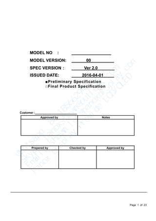
  • 1. Page 1 of 23 MODEL NO : MODEL VERSION: 00 SPEC VERSION : Ver 2.0 ISSUED DATE: 2016-04-01 ■Preliminary Specification □Final Product Specification Customer : Approved by Notes Prepared by Checked by Approved by W h a t s a p p :   8 6   1 8 5 6 6 2 9 4 2 1 8 S k y p e :   p a n o x s h a w n @ o u t l o o k . c o m E m a i l :   s h a w n . l e e @ p a n o x d i s p l a y . c o m P a n o x   D i s p l a y   P r o v i d e   L C D / O L E D
  • 2. Page 2 of 23 Table of Contents Table of Contents .............................................................................................................................. 2 Record of Revision............................................................................................................................ 3 1 General Specifications ............................................................................................................... 4 2 Input/Output Terminals............................................................................................................... 5 2.1 LCD interface............................................................................................................................5 2.2 CTP interfcae............................................................................................................................6 3 Absolute Maximum Ratings ....................................................................................................... 7 4 Electrical Characteristics............................................................................................................ 7 4.1 LCD characteristics..................................................................................................................7 4.2 BL characteristics......................................................................................................................8 5 Timing Chart............................................................................................................................... 9 6 Optical Characteristics ............................................................................................................. 15 7 Environmental / Reliability Test ................................................................................................ 18 8 Mechanical Drawing................................................................................................................. 19 9 Packing Drawing ...................................................................................................................... 20 10 Precautions for Use of LCD Modules....................................................................................... 23 W h a t s a p p :   8 6   1 8 5 6 6 2 9 4 2 1 8 S k y p e :   p a n o x s h a w n @ o u t l o o k . c o m E m a i l :   s h a w n . l e e @ p a n o x d i s p l a y . c o m P a n o x   D i s p l a y   P r o v i d e   L C D / O L E D
  • 3. Page 3 of 23 Record of Revision Rev Issued Date Description Editor 1.0 2015-12-29 Preliminary Specification Release Xunqiang Ji 2.0 2016-04-01 Modify Mechanical Drawing & Add Packing Drawing Xunqiang Ji W h a t s a p p :   8 6   1 8 5 6 6 2 9 4 2 1 8 S k y p e :   p a n o x s h a w n @ o u t l o o k . c o m E m a i l :   s h a w n . l e e @ p a n o x d i s p l a y . c o m P a n o x   D i s p l a y   P r o v i d e   L C D / O L E D
  • 4. Page 4 of 23 1 General Specifications Feature Spec Display Spec. Size 3.4 inch Resolution 800(RGB) x 800 Technology Type a-Si Pixel Configuration R.G.B. Vertical Stripe Pixel pitch(um) 109.5*109.5 Display Mode SFT Surface Treatment HC Viewing Direction FREE Mechanical Characteristics Module (W x H x D) (mm) with CTP 99.0 x 96.6 x 3.98 Active Area(mm) 87.6*87.6 With /Without TSP With CTP Matching Connection Type FPC LED Numbers 8 LEDs CTP Surface hardness ≥7H Weight (g) TBD Electrical Characteristics Interface MIPI 3 lane Color Depth 16.7M LCD Driver IC ILI9881C CTP Driver IC HX8526-E30 CTP Interface IIC Note 1: Viewing direction for best image quality is different from TFT definition. There is a 180 degree shift. Note 2: Requirements on Environmental Protection: Q/S0002 Note 3: LCM weight tolerance: ± 5% W h a t s a p p :   8 6   1 8 5 6 6 2 9 4 2 1 8 S k y p e :   p a n o x s h a w n @ o u t l o o k . c o m E m a i l :   s h a w n . l e e @ p a n o x d i s p l a y . c o m P a n o x   D i s p l a y   P r o v i d e   L C D / O L E D
  • 5. Page 5 of 23 2 Input/Output Terminals 2.1 LCD Interface Pin No. Symbol I/O Function Remark 1 GND GND Power Ground 2 LEDA P LED Anode 3 LEDA P 4 LEDK P LED Cathode 5 LEDK P 6 GND GND Power Ground 7 VDD(-5V) P -5V INPUT 8 VDD(-5V) P 9 GND GND Power Ground 10 VDD(+5V) P +5V INPUT 11 VDD(+5V) P 12 GND GND Power Ground 13 IOVCC P Power supply 1.8V 14 IOVCC P 15 GND GND Power Ground 16 RESET I Global Reset Pin 17 GND GND Power Ground 18 TE I tearing effect output 19 GND GND Power Ground 20 NC N No connect 21 NC N 22 NC N 23 GND GND Power Ground 24 LAN2_P I MIPI lane 2+ 25 NC N No connect 26 LAN2_N I MIPI lane 2- 27 GND GND Power Ground 28 CLK_P I MIPI clock + 29 NC N No connect W h a t s a p p :   8 6   1 8 5 6 6 2 9 4 2 1 8 S k y p e :   p a n o x s h a w n @ o u t l o o k . c o m E m a i l :   s h a w n . l e e @ p a n o x d i s p l a y . c o m P a n o x   D i s p l a y   P r o v i d e   L C D / O L E D
  • 6. Page 6 of 23 30 CLK_N I IMIPI clock - 31 GND GND Power Ground 32 LAN1_P I MIPI lane 1+ 33 NC N No connect 34 LAN1_N I MIPI lane 1- 35 GND GND Power Ground 36 LAN0_P I MIPI lane 0+ 37 NC N No connect 38 LAN0_N I MIPI lane 0- 39 GND GND Power Ground 2.2 CTP Interface Pin Name 1 VCCA(2.8V) 2 VCCD(1.8V) 3 SCL 4 SDA 5 GND 6 GND 7 TSIX 8 NC 9 NC 10 XRES W h a t s a p p :   8 6   1 8 5 6 6 2 9 4 2 1 8 S k y p e :   p a n o x s h a w n @ o u t l o o k . c o m E m a i l :   s h a w n . l e e @ p a n o x d i s p l a y . c o m P a n o x   D i s p l a y   P r o v i d e   L C D / O L E D
  • 7. Page 7 of 23 3 Absolute Maximum Ratings GND=0V Item Symbol MIN MAX Unit Remark Power Supply Voltage IOVCC -0.3 3.3 V Note1 Power Supply Voltage VDD(+5V) -0.3 6.5 Power Supply Voltage VDD(-5V) -6.5 0.3 Logic Supply Voltage VCCIO -0.3 3.3 V Operating Temperature Top -20 70 ℃ Storage Temperature Tst -30 80 ℃ Relative Humidity Note2 RH -- ≤95 % Ta≤40℃ -- ≤85 % 40℃<Ta≤50℃ -- ≤55 % 50℃<Ta≤60℃ -- ≤36 % 60℃<Ta≤70℃ -- ≤24 % 70℃<Ta≤80℃ Absolute Humidity AH -- ≤70 g/m³ Ta>70℃ Table 3 Absolute Maximum Ratings Note1: Input voltage include R0~R5, G0~G5, B0~B5, Dotclk, Hsync, Vsync, Enable, R/L, U/D. 4 Electrical Characteristics 4.1 LCD characteristics GND=0V,Ta=25℃ Item Symbol MIN TYP MAX Unit Remark Power Supply Voltage IOVCC 1.75 1.8 3.3 V Power Supply Voltage VDD(+5V) 4.5 5.0 6 V Power Supply Voltage VDD(-5V) -6 -5.0 -4.5 Input Signal Voltage High Level VIH 0.7*IOVCC - IOVCC V Low Level VIL 0 - 0.3*IOVCC V Table 4.1 LCD module electrical characteristics W h a t s a p p :   8 6   1 8 5 6 6 2 9 4 2 1 8 S k y p e :   p a n o x s h a w n @ o u t l o o k . c o m E m a i l :   s h a w n . l e e @ p a n o x d i s p l a y . c o m P a n o x   D i s p l a y   P r o v i d e   L C D / O L E D
  • 8. Page 8 of 23 4.2 Backlight Unit Ta=25℃ Item Symbol Min Typ Max Unit Remark Forward Current IF 18 20 22 mA 1 LED Forward Voltage VF - 12.8 - V BLH-BLL Backlight Power Consumption WBL - 512 - mW 8 LEDs Operating Life Time - - 30,000 - Hrs For each LED Note1: Figure below shows the connection of backlight LED. Note 2: 1LED: VF =3.2V IF =20mA Note 3: IF is defined for one LED. Optical performance should be evaluated at Ta=25℃ only. If LED is driven by high current, high ambient temperature & humidity condition. The life time of LED will be reduced. Operating life means brightness goes down to 50% initial brightness. Typical operating life time is estimated data. LED CIRCUIT LED K LED A (If=40mA / Vf=12.8V TYP) W h a t s a p p :   8 6   1 8 5 6 6 2 9 4 2 1 8 S k y p e :   p a n o x s h a w n @ o u t l o o k . c o m E m a i l :   s h a w n . l e e @ p a n o x d i s p l a y . c o m P a n o x   D i s p l a y   P r o v i d e   L C D / O L E D
  • 9. Page 9 of 23 5 Timing Chart 5.1 MIPI Data to clock Timing Definition 5.1.1 High Speed Mode W h a t s a p p :   8 6   1 8 5 6 6 2 9 4 2 1 8 S k y p e :   p a n o x s h a w n @ o u t l o o k . c o m E m a i l :   s h a w n . l e e @ p a n o x d i s p l a y . c o m P a n o x   D i s p l a y   P r o v i d e   L C D / O L E D
  • 10. Page 10 of 23 W h a t s a p p :   8 6   1 8 5 6 6 2 9 4 2 1 8 S k y p e :   p a n o x s h a w n @ o u t l o o k . c o m E m a i l :   s h a w n . l e e @ p a n o x d i s p l a y . c o m P a n o x   D i s p l a y   P r o v i d e   L C D / O L E D
  • 11. Page 11 of 23 5.1.2 Low Speed Mode W h a t s a p p :   8 6   1 8 5 6 6 2 9 4 2 1 8 S k y p e :   p a n o x s h a w n @ o u t l o o k . c o m E m a i l :   s h a w n . l e e @ p a n o x d i s p l a y . c o m P a n o x   D i s p l a y   P r o v i d e   L C D / O L E D
  • 12. Page 12 of 23 W h a t s a p p :   8 6   1 8 5 6 6 2 9 4 2 1 8 S k y p e :   p a n o x s h a w n @ o u t l o o k . c o m E m a i l :   s h a w n . l e e @ p a n o x d i s p l a y . c o m P a n o x   D i s p l a y   P r o v i d e   L C D / O L E D
  • 13. Page 13 of 23 W h a t s a p p :   8 6   1 8 5 6 6 2 9 4 2 1 8 S k y p e :   p a n o x s h a w n @ o u t l o o k . c o m E m a i l :   s h a w n . l e e @ p a n o x d i s p l a y . c o m P a n o x   D i s p l a y   P r o v i d e   L C D / O L E D
  • 14. Page 14 of 23 5.2 Timing for DSI video mode 5.3 Reset Timing W h a t s a p p :   8 6   1 8 5 6 6 2 9 4 2 1 8 S k y p e :   p a n o x s h a w n @ o u t l o o k . c o m E m a i l :   s h a w n . l e e @ p a n o x d i s p l a y . c o m P a n o x   D i s p l a y   P r o v i d e   L C D / O L E D
  • 15. Page 15 of 23 6 Optical Characteristics 6.1 Driving the backlight condition Item Symbol Condition Min Typ Max Unit Remark View Angles θT CR 10 ≧ 70 80 -- Degree Note2 θB 70 80 -- θL 70 80 -- θR 70 80 -- Contrast Ratio CR θ=0o 600 800 -- Note 3 Response Time TON 25℃ -- 25 35 ms Note 4 TOFF Chromaticity White x Backlight is on 0.263 0.313 0.363 Note 1,5 y 0.279 0.329 0.379 Red x -- TBD -- Note 1,5 y -- TBD -- Green x -- TBD -- Note 1,5 y -- TBD -- Blue x -- TBD -- Note 1,5 y -- TBD -- Uniformity U 75 80 -- % Note 6 NTSC 65 70 -- % Note 5 Luminance L 280 350 -- cd/m2 Note 7 Test Conditions: 1. IF= 20 mA(one LED), and the ambient temperature is 25 . ℃ 2. The test systems refer to Note 1 and Note 2. W h a t s a p p :   8 6   1 8 5 6 6 2 9 4 2 1 8 S k y p e :   p a n o x s h a w n @ o u t l o o k . c o m E m a i l :   s h a w n . l e e @ p a n o x d i s p l a y . c o m P a n o x   D i s p l a y   P r o v i d e   L C D / O L E D
  • 16. Page 16 of 23 Note 1: Definition of optical measurement system. The optical characteristics should be measured in dark room. After 5 Minutes operation, the optical properties are measured at the center point of the LCD screen. All input terminals LCD panel must be ground when measuring the center area of the panel. Note 2: Definition of viewing angle range and measurement system. viewing angle is measured at the center point of the LCD by CONOSCOPE(ergo-80)。 Note 3: Definition of contrast ratio “White state “: The state is that the LCD should drive by Vwhite. Item Photo detector Field Contrast Ratio SR-3A 1° Luminance Chromaticity Lum Uniformity Response Time BM-7A 2° 500mm Photo detector Field LCD Panel TFT-LCD Module The center of the screen W h a t s a p p :   8 6   1 8 5 6 6 2 9 4 2 1 8 S k y p e :   p a n o x s h a w n @ o u t l o o k . c o m E m a i l :   s h a w n . l e e @ p a n o x d i s p l a y . c o m P a n o x   D i s p l a y   P r o v i d e   L C D / O L E D
  • 17. Page 17 of 23 “Black state”: The state is that the LCD should drive by Vblack. Vwhite: To be determined Vblack: To be determined. Note 4: Definition of Response time The response time is defined as the LCD optical switching time interval between “White” state and “Black” state. Rise time (TON) is the time between photo detector output intensity changed from 90% to 10%. And fall time (TOFF) is the time between photo detector output intensity changed from 10% to 90%. Note 5: Definition of color chromaticity (CIE1931) Color coordinates measured at center point of LCD. Note 6: Definition of Luminance Uniformity Active area is divided into 9 measuring areas (Refer Fig. 2). Every measuring point is placed at the center of each measuring area. Luminance Uniformity (U) = Lmin/ Lmax L-------Active area length W----- Active area width Lmax: The measured Maximum luminance of all measurement position. Lmin: The measured Minimum luminance of all measurement position. Note 7: Definition of Luminance: Measure the luminance of white state at center point. W h a t s a p p :   8 6   1 8 5 6 6 2 9 4 2 1 8 S k y p e :   p a n o x s h a w n @ o u t l o o k . c o m E m a i l :   s h a w n . l e e @ p a n o x d i s p l a y . c o m P a n o x   D i s p l a y   P r o v i d e   L C D / O L E D
  • 18. Page 18 of 23 7 Environmental / Reliability Test No Test Item Condition Remarks 1 High Temperature Operation Ts=+70℃, 120hrs Restore 2H at 25℃ Power off IEC60068-2-1:2007 GB2423.2-2008 2 Low Temperature Operation Ta=-20℃, 120hrs Restore 2H at 25℃ Power off IEC60068-2-1:2007 GB2423.1-2008 3 High Temperature Storage Ta=+80℃, 120hrs Restore 2H at 25℃ Power off IEC60068-2-1:2007 GB2423.2-2008 4 Low Temperature Storage Ta=-30℃, 120hrs Restore 2H at 25℃ Power off IEC60068-2-1:2007 GB2423.1-2008 5 Storage at High Temperature and Humidity Ta=+60℃, 90% RH, 120 hours Restore 2H at 25℃ Power off IEC60068-2-78 :2001 GB/T2423.3—2006 7 ESD Sensitivity test C=150pF, R=330Ω,5points/panel Air:± 8KV, 5times, Contact:± 4KV, 5 times, (Environment: 15℃~35℃, 30%~60%, 86Kpa~106Kpa) IEC61000-4-2:2001 GB/T17626.2-2006 Note1: Ts is the temperature of panel’s surface. Note2: Ta is the ambient temperature of sample. Note3: Before cosmetic and function test, the product must have enough recovery time, at least 2 hours at room temperature. Note 4: In the standard condition, there shall be no practical problem that may affect the display function. After the reliability test, the product only guarantees operation, but don’t guarantee all of the cosmetic specification. W h a t s a p p :   8 6   1 8 5 6 6 2 9 4 2 1 8 S k y p e :   p a n o x s h a w n @ o u t l o o k . c o m E m a i l :   s h a w n . l e e @ p a n o x d i s p l a y . c o m P a n o x   D i s p l a y   P r o v i d e   L C D / O L E D
  • 19. Page 19 of 23 8 Mechanical Drawing 2.25±0.15 2.10±0.15 1.10±0.15 1.00±0.15 0.30±0.15 0.30 +0.04 -0.03 0.10±0.03 0.60±0.07 10.80±0.05 R 0 . 2 0 0.30 +0.04 -0.03 0.60±0.03 0.30±0.03 0.30±0.07 11.40±0.05 12.00±0.1 0.1095 0.1095 Notes: 1.LCM Display Type: A-Si SFT; CTP: GFF 2.LCM Drive IC: ILI9881C; CTP Drive IC: HX8526-E30 3.View Direction: ALL 4.LCM Matched Connector: FH26W-39S-0.3SHW CTP Matched Connector: OK-22F010-04 5.General Tolerance: ±0.2 6.Operation Temp: -20°~+70°C Storage Temp: -30°~+80°C 7.Requirements on Environment Protection: Q/S0002 1.20 1.00 MAX(CTP) 99.00 47.30 1.00 MAX(LCM) 0.20±0.05 3.98±0.3 1.10±0.05(LENS) 1.35±0.1(CTP) 0.175(OCA) 0.50±0.1 34.70±0.5 ? 96.60(LCM) ? 96.00(CTP O.D) ? 92.00( 上台阶) ? 88.60(CTP V.A) ? 87.60(LCD A.A) 2.45(LCM) 32.40±0.5 (0.20) 2.60±0.3 4.00±0.5 12.42±0.5 2.50±0.3 YGT1-01 LCM+CTP Chen HuiXuan Liu Junwei An Guangkun 0 2016.03.30 Feng SongLin PIN NAME 2 3 4 5 6 7 8 9 10 1 VCCA(2.8V) VCCD(1.8V) LCM CTP XRES R G B DOTS DETAIL Insulation Tape Component Area Bending Area No. Symbol 2 3 4 5 6 7 8 9 10 11 12 13 14 15 16 17 18 19 20 21 22 23 24 1 25 26 27 28 29 30 GND LEDA LEDK GND NC NC GND GND GND LAN2_N VDD(-5V) TE VDD(+5V) IOVCC(1.8V) RESET LAN2_P CLK_P CLK_N GND LAN1_P LAN1_N 31 32 33 34 GND LAN0_P LAN0_N GND GND 35 36 37 38 39 GND GND GND NC NC NC NC NC IOVCC(1.8V) VDD(+5V) VDD(-5V) LEDA LEDK NC NC TSIX GND GND SDA SCL Printing Black 800(RGB)X800 3.4" TFT Shield SUS304 CTP Connecter SUS304 Shield (If=40mA / Vf=12.8V TYP) PI 1 39 XXXXXXXXXXXX (LCM) 1 39 A A K XXXXXXXXXXXX (BL) (OK-22M010-04) 2016.03.30 2016.03.30 2016.03.30 1 . 0 0 W h a t s a p p :   8 6   1 8 5 6 6 2 9 4 2 1 8 S k y p e :   p a n o x s h a w n @ o u t l o o k . c o m E m a i l :   s h a w n . l e e @ p a n o x d i s p l a y . c o m P a n o x   D i s p l a y   P r o v i d e   L C D / O L E D
  • 20. Page 20 of 23 9 Packing Drawing 9.1 Per Carton 9.2 Packaging Specification and Quantity W h a t s a p p :   8 6   1 8 5 6 6 2 9 4 2 1 8 S k y p e :   p a n o x s h a w n @ o u t l o o k . c o m E m a i l :   s h a w n . l e e @ p a n o x d i s p l a y . c o m P a n o x   D i s p l a y   P r o v i d e   L C D / O L E D
  • 21. Page 21 of 23 9.3 Packing Form W h a t s a p p :   8 6   1 8 5 6 6 2 9 4 2 1 8 S k y p e :   p a n o x s h a w n @ o u t l o o k . c o m E m a i l :   s h a w n . l e e @ p a n o x d i s p l a y . c o m P a n o x   D i s p l a y   P r o v i d e   L C D / O L E D
  • 22. Page 22 of 23 9.4 Shipping Package of Palletizing Sequence 纸箱堆叠数按 2×3/每层×共 5 层  W h a t s a p p :   8 6   1 8 5 6 6 2 9 4 2 1 8 S k y p e :   p a n o x s h a w n @ o u t l o o k . c o m E m a i l :   s h a w n . l e e @ p a n o x d i s p l a y . c o m P a n o x   D i s p l a y   P r o v i d e   L C D / O L E D
  • 23. Page 23 of 23 10 Precautions for Use of LCD Modules 10.1 Handling Precautions 10.1.1 The display panel is made of glass. Do not subject it to a mechanical shock by dropping it from a high place, etc. 10.1.2 If the display panel is damaged and the liquid crystal substance inside it leaks out, be sure not to get any in your mouth, if the substance comes into contact with your skin or clothes, promptly wash it off using soap and water. 10.1.3 Do not apply excessive force to the display surface or the adjoining areas since this may cause the color tone to vary. 10.1.4 The polarizer covering the display surface of the LCD module is soft and easily scratched. Handle this polarizer carefully. 10.1.5 If the display surface is contaMinated, breathe on the surface and gently wipe it with a soft dry cloth. If still not completely clear, moisten cloth with one of the following solvents: - Isopropyl alcohol - Ethyl alcohol Solvents other than those mentioned above may damage the polarizer. Especially, do not use the following: - Water - Ketone - Aromatic solvents 10.1.6 Do not attempt to disassemble the LCD Module. 10.1.7 If the logic circuit power is off, do not apply the input signals. 10.1.8 To prevent destruction of the elements by static electricity, be careful to maintain an optimum work environment. 10.1.8.1 Be sure to ground the body when handling the LCD Modules. 10.1.8.2 Tools required for assembly, such as soldering irons, must be properly ground. 10.1.8.3 To reduce the amount of static electricity generated, do not conduct assembly and other work under dry conditions. 10.1.8.4 The LCD Module is coated with a film to protect the display surface. Be care when peeling off this protective film since static electricity may be generated. 10.2 Storage precautions 10.2.1 When storing the LCD modules, avoid exposure to direct sunlight or to the light of fluorescent lamps. 10.2.2 The LCD modules should be stored under the storage temperature range. If the LCD modules will be stored for a long time, the recommend condition is: Temperature : 0℃ ~ 40℃ Relatively humidity: ≤80% 10.2.3 The LCD modules should be stored in the room without acid, alkali and harmful gas. 10.3 Transportation Precautions 10.3.1 The LCD modules should be no falling and violent shocking during transportation, and also should avoid excessive press, water, damp and sunshine. W h a t s a p p :   8 6   1 8 5 6 6 2 9 4 2 1 8 S k y p e :   p a n o x s h a w n @ o u t l o o k . c o m E m a i l :   s h a w n . l e e @ p a n o x d i s p l a y . c o m P a n o x   D i s p l a y   P r o v i d e   L C D / O L E D