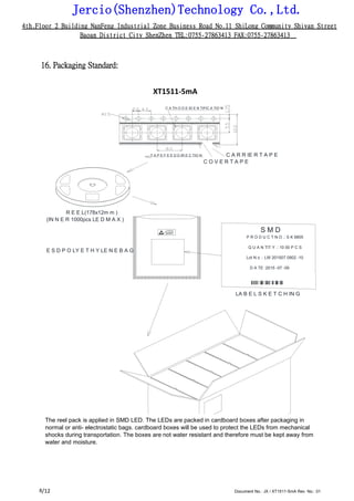
Cloud Frontiers: A Deep Dive into Serverless Spatial Data and FME
Xt1511 5m a rev.01 en(nut)
1. Jercio(Shenzhen)Technology Co.,Ltd.
4th.Floor 2 Building NanFeng Industrial Zone Business Road No.11 ShiLong Community Shiyan Street
Baoan District City ShenZhen TEL:0755-27863413 FAX:0755-27863413
/12 Document No.: JX / XT1511-5mA Rev.
No.: 01
1
XT1511-5mA
SPECIFICATION
INTEGRATED LIGHT SOURCE INTELLIGENT CONTROL OF
CHIP-ON-TOP SMD TYPE LED
Document No.: JX/ XT1511-5mA
Model No.: XT1511-5mA
Description: 5.5x5.0x1.6mm Top SMD Type 0.2Watt Power tegrated
light source Intelligent control LED
Rev. No.: 01
Date: 2016-01-08
ELECTROSTATIC
SENSITIVE DEVICES
2. Jercio(Shenzhen)Technology Co.,Ltd.
4th.Floor 2 Building NanFeng Industrial Zone Business Road No.11 ShiLong Community Shiyan Street
Baoan District City ShenZhen TEL:0755-27863413 FAX:0755-27863413
/12 Document No.: JX / XT1511-5mA Rev.
No.: 01
2
INTEGRATED LIGHT SOURCE INTELLIGENT CONTROL
OF CHIP-ON-TOP SMD TYPE LED
Model: XT1511-5mA
1. Product Overview :
XT1511-5mA is a smart LED control circuit and light emitting circuit in one controlled LED source,
which has the shape of a 5050 LED chip. Each lighting element is a pixel, and the intensities of the
pixels are contained within the intelligent digital interface input. The output is driven by patented
PWM technology, which effectively guarantees high consistency of the color of the pixels. The control
circuit consists of a signal shaping amplification circuit, a built-in constant current circuit, and a high
precision RC oscillator.
The data protocol being used is unipolar NRZ communication mode. The 24-bit data is transmitted
from the controller to DIN of the first element, and if it is accepted it is extracted pixel to pixel. After an
internal data latch, the remaining data is passed through the internal amplification circuit and sent out
on the DO port to the remaining pixels. The pixel is reset after the end of DIN. Using automatic shaping
forwarding technology makes the number of cascaded pixels without signal transmission only limited
by signal transmission speed.
The LED has a low driving voltage (which allows for environmental protection and energy saving),
high brightness, scattering angle, good consistency, low power, and long life. The control circuit is
integrated in the LED above.
2. Main Application Field:
● Full color LED string light, LED full color module, LED super hard and soft lights, LED guardrail tube,
LED appearance / scene lighting
● LED point light, LED pixel screen, LED shaped screen, a variety of electronic products,
electrical equipment etc..
3. Description:
● Top SMD internal integrated high quality external control line serial cascade constant current IC;
● control circuit and the RGB chip in SMD 5050 components, to form a complete control of pixel, color
mixing uniformity and consistency;
●built-in data shaping circuit, a pixel signal is received after wave shaping and output
waveform distortion will not guarantee a line;
●The built-in power on reset and reset circuit, the power does not work;
●gray level adjusting circuit (256 level gray scale adjustable);
● red drive special treatment, color balance;
● line data transmission;
● plastic forward strengthening technology, the transmission distance between two points over 10M;
●Using a typical data transmission frequency of 800 Kbps, when the refresh rate of 30 frames per sec
3. Jercio(Shenzhen)Technology Co.,Ltd.
4th.Floor 2 Building NanFeng Industrial Zone Business Road No.11 ShiLong Community Shiyan Street
Baoan District City ShenZhen TEL:0755-27863413 FAX:0755-27863413
/12 Document No.: JX / XT1511-5mA Rev.
No.: 01
3
4. Mechanical Dimensions:
Notes:
1. All dimensions are in millimeters.
2. Tolerance is ±0.1mm unless otherwise noted
5. PIN configuration
NO. Symbol Function description
1 VDD Power supply LED
2 DOUT Control data signal output
3 VSS Ground
4 DIN Control data signal input
6. General Information
XT1511-5mA
XT: The default is RGB chips with IC integration
4. Jercio(Shenzhen)Technology Co.,Ltd.
4th.Floor 2 Building NanFeng Industrial Zone Business Road No.11 ShiLong Community Shiyan Street
Baoan District City ShenZhen TEL:0755-27863413 FAX:0755-27863413
/12 Document No.: JX / XT1511-5mA Rev. No.:
01
4
7. Absolute Maximum Ratings(Ta=25℃,VSS=0V) :
Parameter Symbol Range Unit
Power supply voltage VDD +3.5~+5.5 V
Logic input voltage
V
IN -0.5~VDD+0.5 V
Working temperature Topt -40~+85 ℃
Storage temperature Tstg -50~+150 ℃
ESD pressure
V
ESD 4K V
8. The electrical parameters (unless otherwise specified, TA=-20 ~ +70 ℃, VDD=4.5 ~ 5.5V,
VSS=0V):
Parmeter Symbol Min Typical Max Unit Test conditions
The chip
VDD --- 5.2 --- V ---
supply voltage
R/G/B port VDS,M
--- --- 26 V ---
pressure AX
DOUT conect ground,
DOUT drive
IDOH --- 49 --- mA the maximum drive
current
capability
IDOL --- -50 --- mA
DOUT conect +, the
largest current
The signal VIH 3.4 --- --- V
input flip VDD=5.0V
VIL --- --- 1.6 Vthreshold
The frequency
FPWM --- 1.2 --- KHZ ---
of PWM
Static power
IDD --- 1 --- mA ---
consumption
9. The dynamic parameters (Ta=25 ℃):
Parameter Symbol Min Typical Max Unit Test conditions
The speed of data
fDIN --- 800 --- KHZ
The duty ratio of 67%
transmission (data 1)
DOUT transmission TPLH --- --- 500 ns
DIN→DOUT
delay TPHL --- --- 500 ns
IOUT Rise/Drop Tr --- 100 --- ns VDS=1.5
Time IOUT=13mATf --- 100 --- ns
5. Jercio(Shenzhen)Technology Co.,Ltd.
4th.Floor 2 Building NanFeng Industrial Zone Business Road No.11 ShiLong Community Shiyan Street
Baoan District City ShenZhen TEL:0755-27863413 FAX:0755-27863413
/12 Document No.: JX / XT1511-5mA Rev. No.:
01
5
10. The data transmission time (TH+TL=1.25µs±600ns):
T0H 0 code, high level time 0.3µs ±0.15µs
T0L 0 code, low level time 0.9µs ±0.15µs
T1H 1 code, high level time 0.6µs ±0.15µs
T1L 1 code, low level time 0.6µs ±0.15µs
Trst Reset code,low level time 80µs
11. Timing waveform:
Input code: Connection mode:
D1 D2 D3 D4DIN DO DIN DO DIN DO
PIX1 PIX2 PIX3
12. The method of data transmission:
Note: the D1 sends data for MCU, D2, D3, D4 for data forwarding automatic shaping cascade circuit.
6. Jercio(Shenzhen)Technology Co.,Ltd.
4th.Floor 2 Building NanFeng Industrial Zone Business Road No.11 ShiLong Community Shiyan Street
Baoan District City ShenZhen TEL:0755-27863413 FAX:0755-27863413
/12 Document No.: JX / XT1511-5mA Rev. No.:
01
6
13. The data structure of 24bit:
G7 G6 G5 G4 G3 G2 G1 G0 R7 R6 R5 R4
R3 R2 R1 R0 B7 B6 B5 B4 B3 B2 B1 B0
Note: high starting, in order to send data (G7 - G6 - ...... ..B0)
14. The typical application circuit:
7. Jercio(Shenzhen)Technology Co.,Ltd.
4th.Floor 2 Building NanFeng Industrial Zone Business Road No.11 ShiLong Community Shiyan Street
Baoan District City ShenZhen TEL:0755-27863413 FAX:0755-27863413
/12 Document No.: JX / XT1511-5mA Rev.
No.: 01
7
15. Standard LED Performance Graph:
Typical Relative Luminous Flux vs. Forward Current Forward Voltage vs. Forward Current
150% 150
120% RED
100%
C
ur
re
nt(
m
A)
RED
BLUE/GREEN 20
80%
60% BLUE/GREEN
40%
Fo
rw
ar
d
10
20%
0.00
10 15 20 150
1
1.0 2.0 3.0 4.0 5.00 50 0.0
Forward Current(mA) Forward Voltage(V) Tj=25 °C
Thermal Pad Temperature vs. Relative Light Output Wavelength Characteristics
Norm
alized
Lumin
ous
Flux
120%
BLUE/GREEN
R
el
ati
ve
E
mi
ssi
on
Di
str
ib
uti
on
100%
GREEN
100%
BLUE
RED80%
80%
60%
RED60%
40%
40%
20% 20%
0.00
20 40 60 80 100 120
0.00
450 500 550 600 650 700 750 8000 400
Thermal Pad Temperature (T=25°C) Wavelength (nm)
Thermal Pad Temperature vs. Forward Current
100
80
Typical Radiation Pattern 120°
0
30°
60
F
or
w
ar
d
C
ur
re
nt
(
m
A)
40
20 RED
0
0 20 40 60 80 100 120 Thermal Pad Temperature (°C)
60°
90°
90 75 60 45 30 15 0 0.2 0.4 0.6 0.8 1.0
Radiation Angle
8. Jercio(Shenzhen)Technology Co.,Ltd.
4th.Floor 2 Building NanFeng Industrial Zone Business Road No.11 ShiLong Community Shiyan Street
Baoan District City ShenZhen TEL:0755-27863413 FAX:0755-27863413
/12 Document No.: JX / XT1511-5mA Rev. No.: 018
16. Packaging Standard:
C A TH O D E ID E N TIFIC A TIO N
T A P E F E E D D IR E C TIO N C A R R IE R T A P E
C O V E R T A P E
R E E L(178x12m m )
(IN N E R 1000pcs LE D M A X )
S M D
P R O D U C T N O .: S K 6805
E S D P O LY E T H Y LE N E B A G
Q U A N TIT Y .: 10 00 P C S
Lot N o .: LW 201507 0902 -10
D A TE :2015 -07 -09
LA B E L S K E T C H IN G
The reel pack is applied in SMD LED. The LEDs are packed in cardboard boxes after packaging in
normal or anti- electrostatic bags. cardboard boxes will be used to protect the LEDs from mechanical
shocks during transportation. The boxes are not water resistant and therefore must be kept away from
water and moisture.
XT1511-5mA
9. Jercio(Shenzhen)Technology Co.,Ltd.
4th.Floor 2 Building NanFeng Industrial Zone Business Road No.11 ShiLong Community Shiyan Street
Baoan District City ShenZhen TEL:0755-27863413 FAX:0755-27863413
/12 Document No.: JX / XT1511-5mA Rev. No.: 019
TOP SMD LED Application Notes
1. Features
The Purposes of making The customers and users to have a clear understanding on the ways how
to use the LED.
2. Description
Generally. The LED can be used the same way as other general purposed semiconductors. When using
The TOP SMD LED, the following precautions must be taken to protect the LED.
3.Cautions
3.1Dust & Cleaning
This emitter has a silicone surface, There are many benefits to the silicone surface in terms of optical
properties and improved reliability. However, silicone is a softer material and prone to attract dust. While a
minimal amount of dust and debris on the LED will not cause significant reduction in illumination, steps
should be taken to keep the emitter free of dust.
These include keeping the LEDs in the manufacturer’s package prior to assembly and storing assemblies
in an enclosed area after installing the emitters.
Surface condition of this device may change when organic solvents such as trichloroethylene or
acetone were applied.
Avoid using organic solvent, it is recommended that isopropyl be used as a solvent for cleaning the LEDs.
When using other solvents, it should be confirmed beforehand whether the solvents will dissolve the
package and the resin of not.
Do not clean the LEDs by the ultrasonic. When it is absolutely necessary, the influence as ultrasonic
cleaning on the LEDs depends on factors such as ultrasonic power. Baking time and assembled condition.
Before cleaning, a pre-test should be done to confirm whether any damage to the LEDs will occur.
3.2. Moisture Proof Package
In order to avoid the absorption of moisture during transportation and storage, LED are packed in the aluminum
envelop, A desiccant is included in the aluminum envelop as it absorbs moisture. When moisture is absorbed
into the AMT package it may vaporize and expand during soldering. There is a possibility that this can cause
exfoliation of the contacts and damage to the optical characteristics of the LEDs. For this reason, the moisture
proof package is used to keep moisture to a minimum in the package.
3.3. Storage
In order to avoid the absorption of moisture, It is recommended to store SMD LED (in bulk or taped) in
the dry box (or the desiccator ) with a desiccant, Otherwise to store them in the following environment as
recommended.
a. Temperature: 5℃~30℃ b. Humidity: 60% RH Max
It is recommended to solder the LED as soon as possible after unpacking the aluminum envelop, But in
case that the LED have to be left unused after unpacking envelop again is requested.
The LED should be soldering within 1 hours after opening the package. If
baking is required, A baking treatment should be performed as follows:
70℃±5℃ for more than 24 hours.
10. Jercio(Shenzhen)Technology Co.,Ltd.
4th.Floor 2 Building NanFeng Industrial Zone Business Road No.11 ShiLong Community Shiyan Street
Baoan District City ShenZhen TEL:0755-27863413 FAX:0755-27863413
/12 Document No.: JX / XT1511-5mA Rev. No.: 0110
3.4. Reflow Soldering Characteristics
In testing, Has found S50 LEDs to be compatible with JEDEC J-STD-020C,using the parameters listed below. As a
general guideline The recommends that users follow the recommended soldering profile provided by the manufacturer of
solder paste used.
Note that this general guideline is offered as a starting point and may require adjustment for certain PCB designs
and Configurations of reflow soldering equipment.
Critical Zone TL to TP
amp-up
L L
(°C
) s max
Te
mp
era
tur
e MIN
Ramp down
ts
(Preheat)
T 25°C to Peak
Times
Profile Feature Lead-Based Solder Lead-Free Solder
Average Ramp-Up Rate (Ts max to Tp ) 3℃/second max. 3℃/second max.
Preheat: Temperature Min (Ts min) 100℃ 150℃
Preheat: Temperature Min (Ts max) 150℃ 200℃
Preheat: Time ( ts min to ts max ) 60-120 seconds 60-180 seconds
Time Maintained Above: Temperature (TL) 183 ℃ 217 ℃
Time Maintained Above: Time (t L) 60-150 seconds 60-150 seconds
Peak/Classification Temperature (T P) 215 ℃ 240 ℃
Time Within 5℃ of Actual Peak Temperature ( tp) <10 seconds <10 seconds
Ramp-Down Rate 6℃/second max. 6℃/second max.
Time 25 ℃ to Peak Temperature <6 minutes max. <6 minutes max.
Note: All temperatures refer to topside of the package, measured on the package body surface.
11. Jercio(Shenzhen)Technology Co.,Ltd.
4th.Floor 2 Building NanFeng Industrial Zone Business Road No.11 ShiLong Community Shiyan Street
Baoan District City ShenZhen TEL:0755-27863413 FAX:0755-27863413
/12 Document No.: JX / XT1511-5mA Rev. No.: 0111
3.5 Heat Generation:
Thermal design of the end product is of paramount importance. Please consider the heat
generation of the LED when making the system design. The coefficient of temperature increase
per input electric power is affected by the thermal resistance of the circuit board and density of
LED placement on the board, as well as components. It is necessary to avoid in tense heat
generation and operate within the maximum rating given in this specification. The operating
current should be decided after considering the ambient maximum temperature of LEDs
3.6 Electrostatic Discharge & Surge Current :
Electrostatic discharge (ESD) or surge current (EOS) may damage LED.
Precautions such as ESD wrist strap, ESD shoe strap or antistatic gloves must be worn
whenever handling of LED.
All devices, equipment and machinery must be properly grounded.
It is recommended to perform electrical test to screen out ESD failures at final inspection. It is
important to eliminate the possibility of surge current during circuitry design.
3.7 Moisture Proof Package
Cannot take any responsibility for any trouble that are caused by using the LEDs at conditions
exceeding our specifications.
The LED light output is strong enough to injure human eyes. Precautions must be taken to
prevent looking directly at the LEDs with unaided eyes for more than a few seconds.
The formal specification must be exchanged and signed by both parties before large volume
purchase begins. The appearance and specifications of the product may be modified for
improvement without notice.
12. Jercio(Shenzhen)Technology Co.,Ltd.
4th.Floor 2 Building NanFeng Industrial Zone Business Road No.11 ShiLong Community Shiyan Street
Baoan District City ShenZhen TEL:0755-27863413 FAX:0755-27863413
/12 Document No.: JX / XT1511-5mA Rev.
No.: 01
12
Change History
FCN No. Date Rev. No. Changes/Reason of changes
2016-01-08 01 Initial Document
Items Signatures Date
Note
Prepared by Kevin Zhu 2016-01-08
Checked by
Approved by
FCN#