Downloaded 11 times
![8/11
SHORT CIRCUIT PROTECTION
The TDA2030has an originalcircuit which limitsthe
current of the output transistors.Fig. 18 showsthat
the maximum output current is a function of the
collector emitter voltage; hence the output transis-
tors work within their safe operating area (Fig. 2).
This function can thereforebe considered as being
peak power limiting rather than simple current lim-
iting.
It reduces the possibility that the devicegets dam-
aged during an accidental short circuit from AC
output to ground.
Figure 1 8. Maximum
output current vs.
voltage [VCEsat] across
each output transistor
Figure 19. Safe operating area and
collector characteristics of the
protected power transistor
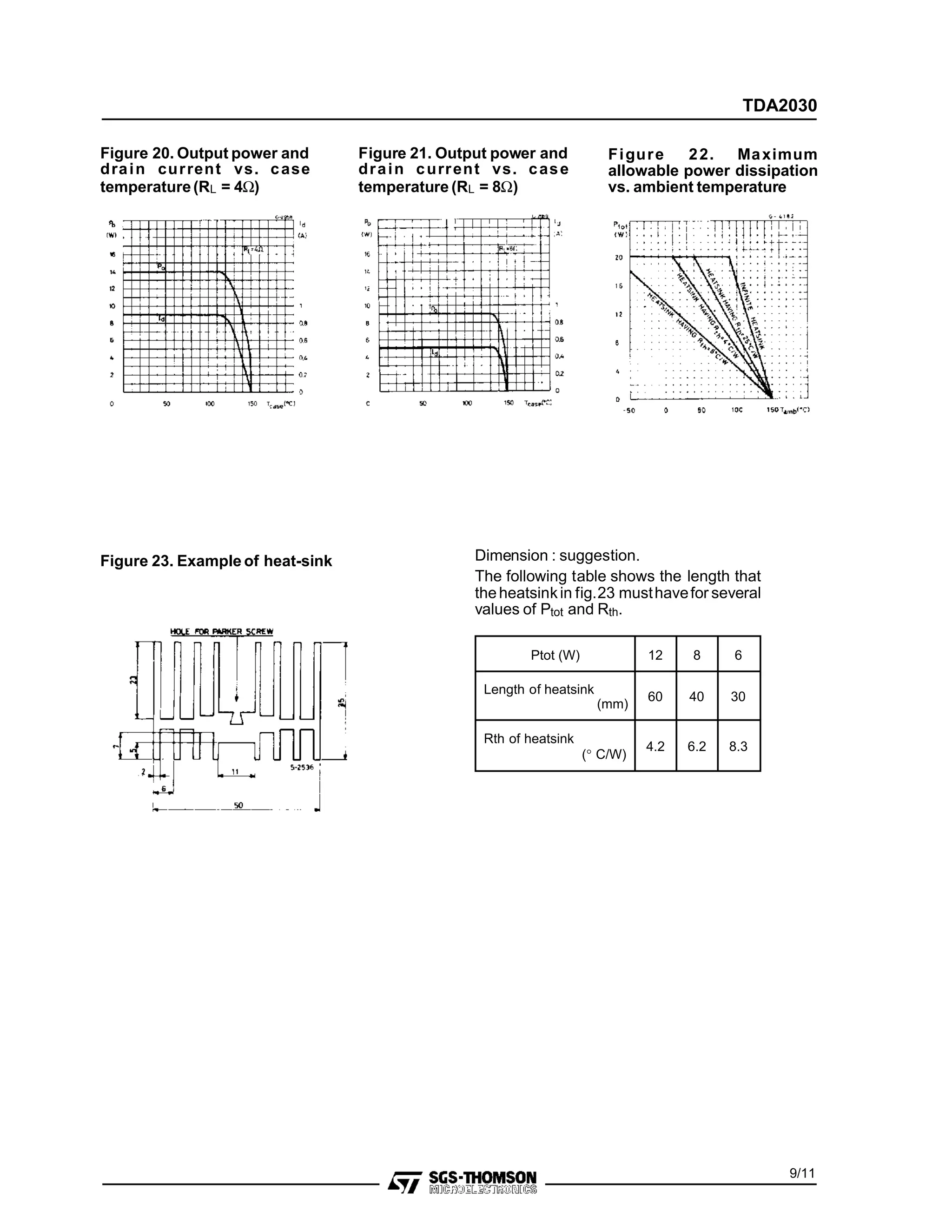
THERMAL SHUT-DOWN
The presenceof a thermal limiting circuit offers the
following advantages:
1. An overload on the output (even if it is perma-
nent), oran abovelimitambienttemperaturecan
be easily supported since the Tj cannot be
higher than 150°C.
2. The heatsinkcan have a smaller factorof safety
compared with that of a conventional circuit.
There is no possibility of device damage due to
high junction temperature.If for any reason, the
junction temperatureincreasesup to 150°C, the
thermal shut-down simply reduces the power
dissipation at the current consumption.
The maximum allowable power dissipation de-
pends upon the size of the external heatsink(i.e.its
thermal resistance); fig. 22 shows this dissipable
power as a function of ambient temperature for
different thermal resistance.
TDA2030](https://image.slidesharecdn.com/tda2030-140328201917-phpapp02/75/Tda-2030-8-2048.jpg)

The TDA2030 is a 14W audio amplifier integrated circuit intended for low frequency class AB amplification. It provides 14W of output power at 14V/4Ω and has very low harmonic and crossover distortion. It also includes an original short circuit protection system to keep the output transistors within their safe operating area and a thermal shutdown system to prevent overheating.


![RF Module Design - [Chapter 6] Power Amplifier](https://cdn.slidesharecdn.com/ss_thumbnails/rfch6-150613070347-lva1-app6891-thumbnail.jpg?width=640&height=640&fit=bounds)


