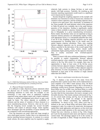
This white paper discusses techniques for mitigating cross-talk in memory arrays as technology scales down to smaller feature sizes. It analyzes the performance of current mode and voltage mode sensing with shielding as feature sizes decrease. Both techniques show increasing read delay and energy consumption due to rising bit-line resistance and coupling capacitance. An alternative technique is proposed that functions as a spatial inverse filter to compensate for cross-talk without these performance penalties during scaling.
![Tagmatech LLC, White Paper: Mitigation of Cross-Talk in Memory Arrays Page 1 of 14
30-Sep-13
Abstract—Cross-talk in memory arrays is a well known and
increasingly important limiter of memory array scaling and
performance. Commonly used techniques for mitigation involve
clever physical layout to cause cross-talk effects to be common
mode between bit-line pairs, combined with differential sensing
circuitry to reject the common mode component. Single-ended
architectures often rely on current mode circuitry or physical
shielding techniques to suppress cross-talk. Proposed here is an
alternative inspired by linear system theory whereby the sensing
circuit functions as a spatial inverse filter that compensates for
cross-talk. It is shown to be effective for a range of memory types,
including those whose signal paths are fundamentally single-
ended rather than differential. Feasibility is demonstrated by
simulation with predictive technology models for a 32nm cmos
memory whose array has very strong bit-line to bit-line coupling.
Comparative advantages are explained in the context of
technology scaling. Applications and further work are suggested.
I. INTRODUCTION
ARASITIC coupling between tightly spaced bit-lines in
memory arrays has been recognized as a limiter of
memory operating margins since the early generations of
DRAM technologies. Due to inherently small signals from
DRAM cells, even low levels of pattern dependent noise from
adjacent line coupling could substantially reduce operating
margins. That led to now well established techniques for
mitigation of the effects in the context of architectures having
differential signal paths [1],[2]. Through physical layout
techniques, unwanted coupling to a differential signal pair can
be made common mode and can then be rejected by a
differential sense amplifier. However, such rejection
techniques tend to waste signal energy increasingly with
technology scaling and, in any case, are not readily
transferrable to architectures that are necessarily single-ended.
Single-ended architectures, based on cross-point cells, have
come to the fore in recent years in the high-density commodity
memory business. The physical simplicity of cross-point cell
layout serves to minimize cost-per-bit, which is paramount in
the design of high density commodity memory products such
as NAND flash. Single-ended signal paths have proven most
compatible with the layout constraints imposed by such high
density array designs. Unfortunately, as memory densities
have increased with improvements in lithography, read mode
delay and energy per read cycle have trended in an
Copyright © 2013 Tagmatech LLC, All Rights Reserved. No licenses, express
or implied, are granted with respect to any technology described herein.
Contact: Bruce L. Morton, P.O. Box 340293, Austin, TX, 78734, USA,
email: bruce.morton@att.net
unfavorable direction.
This paper first shows the cause of the negative
performance trend in single-ended architectures is cross-talk
due to parasitic coupling between physically proximate signal
paths, combined with the inherent properties of conventional
single-ended circuit techniques. It is demonstrated that both
current mode sensing and voltage mode with shielding are
effective in suppressing cross-talk, but both exhibit degraded
performance as feature sizes shrink. Then an alternate
technique is proposed for sensing stored states in the presence
of strong cross-talk. The technique is based on the notion that
cross-talk is systematic spatial distortion of signal paths that
can be received as-is at a memory sense amplifier, where the
effects can be filtered out. With the proposed technique, delay
and energy are shown to trend downward with feature size
scaling, in stark contrast to commonly used techniques. The
proposed technique is also shown to work well in an all-bit-
line type of architecture where conventional voltage level
sensing would be unworkable due to a negative signal margin
caused by strong cross-talk. Extension of the concept to
applications with differential signal paths is also outlined.
II. MODELING MEMORY ARRAY SCALING EFFECTS
A. Physical Structure of Memory Array Interconnect
Referring to Fig. 1(a), signal paths in memory IC’s use
conductors having spacing, S, width, W, and thickness, T,
combined with a vertical separation, H, from any structure that
functions as a ground plane. The illustration is general, but is
proportioned to suggest recent memory technologies where W
and S can be small relative to the other dimensions. It is in
such situations that the value of the lateral coupling
capacitance, Cc, becomes large relative to the value of
capacitance to ground, Cg. In a memory array so constructed,
signals from a memory data storage element, passing through
a bit-line in the direction, L, can be strongly influenced by
signals developed on neighboring bit-lines.
B. An Array Model
A very basic memory array model that comprehends the
primary effects is shown in Fig. 1(b). A memory device on a
bit-line is modeled as a resistance whose value is RDATA,
where the resistance value encodes stored data. For the
analyses in this work, RDATA is set to 500K ohms to
represent cells in a conductive state and 50MΩ for cells in the
non-conductive state. In principle, additional states could be
encoded by defining additional valid ranges, as in some
commercial multi-state cells, but the binary case suffices for
this study. The idealized cell access switches are modeled with
Mitigation of Cross-Talk in Memory Arrays
Bruce L. Morton
Tagmatech LLC
P](https://image.slidesharecdn.com/1a483f85-6694-49be-97a6-2a5e8dedc419-161009211542/85/Mitigation-of-Cross-Talk-in-Memory-Arrays-1-320.jpg)
![Tagmatech LLC, White Paper: Mitigation of Cross-Talk in Memory Arrays Page 1 of 14
30-Sep-13
Abstract—Cross-talk in memory arrays is a well known and
increasingly important limiter of memory array scaling and
performance. Commonly used techniques for mitigation involve
clever physical layout to cause cross-talk effects to be common
mode between bit-line pairs, combined with differential sensing
circuitry to reject the common mode component. Single-ended
architectures often rely on current mode circuitry or physical
shielding techniques to suppress cross-talk. Proposed here is an
alternative inspired by linear system theory whereby the sensing
circuit functions as a spatial inverse filter that compensates for
cross-talk. It is shown to be effective for a range of memory types,
including those whose signal paths are fundamentally single-
ended rather than differential. Feasibility is demonstrated by
simulation with predictive technology models for a 32nm cmos
memory whose array has very strong bit-line to bit-line coupling.
Comparative advantages are explained in the context of
technology scaling. Applications and further work are suggested.
I. INTRODUCTION
ARASITIC coupling between tightly spaced bit-lines in
memory arrays has been recognized as a limiter of
memory operating margins since the early generations of
DRAM technologies. Due to inherently small signals from
DRAM cells, even low levels of pattern dependent noise from
adjacent line coupling could substantially reduce operating
margins. That led to now well established techniques for
mitigation of the effects in the context of architectures having
differential signal paths [1],[2]. Through physical layout
techniques, unwanted coupling to a differential signal pair can
be made common mode and can then be rejected by a
differential sense amplifier. However, such rejection
techniques tend to waste signal energy increasingly with
technology scaling and, in any case, are not readily
transferrable to architectures that are necessarily single-ended.
Single-ended architectures, based on cross-point cells, have
come to the fore in recent years in the high-density commodity
memory business. The physical simplicity of cross-point cell
layout serves to minimize cost-per-bit, which is paramount in
the design of high density commodity memory products such
as NAND flash. Single-ended signal paths have proven most
compatible with the layout constraints imposed by such high
density array designs. Unfortunately, as memory densities
have increased with improvements in lithography, read mode
delay and energy per read cycle have trended in an
Copyright © 2013 Tagmatech LLC, All Rights Reserved. No licenses, express
or implied, are granted with respect to any technology described herein.
Contact: Bruce L. Morton, P.O. Box 340293, Austin, TX, 78734, USA,
email: bruce.morton@att.net
unfavorable direction.
This paper first shows the cause of the negative
performance trend in single-ended architectures is cross-talk
due to parasitic coupling between physically proximate signal
paths, combined with the inherent properties of conventional
single-ended circuit techniques. It is demonstrated that both
current mode sensing and voltage mode with shielding are
effective in suppressing cross-talk, but both exhibit degraded
performance as feature sizes shrink. Then an alternate
technique is proposed for sensing stored states in the presence
of strong cross-talk. The technique is based on the notion that
cross-talk is systematic spatial distortion of signal paths that
can be received as-is at a memory sense amplifier, where the
effects can be filtered out. With the proposed technique, delay
and energy are shown to trend downward with feature size
scaling, in stark contrast to commonly used techniques. The
proposed technique is also shown to work well in an all-bit-
line type of architecture where conventional voltage level
sensing would be unworkable due to a negative signal margin
caused by strong cross-talk. Extension of the concept to
applications with differential signal paths is also outlined.
II. MODELING MEMORY ARRAY SCALING EFFECTS
A. Physical Structure of Memory Array Interconnect
Referring to Fig. 1(a), signal paths in memory IC’s use
conductors having spacing, S, width, W, and thickness, T,
combined with a vertical separation, H, from any structure that
functions as a ground plane. The illustration is general, but is
proportioned to suggest recent memory technologies where W
and S can be small relative to the other dimensions. It is in
such situations that the value of the lateral coupling
capacitance, Cc, becomes large relative to the value of
capacitance to ground, Cg. In a memory array so constructed,
signals from a memory data storage element, passing through
a bit-line in the direction, L, can be strongly influenced by
signals developed on neighboring bit-lines.
B. An Array Model
A very basic memory array model that comprehends the
primary effects is shown in Fig. 1(b). A memory device on a
bit-line is modeled as a resistance whose value is RDATA,
where the resistance value encodes stored data. For the
analyses in this work, RDATA is set to 500K ohms to
represent cells in a conductive state and 50MΩ for cells in the
non-conductive state. In principle, additional states could be
encoded by defining additional valid ranges, as in some
commercial multi-state cells, but the binary case suffices for
this study. The idealized cell access switches are modeled with
Mitigation of Cross-Talk in Memory Arrays
Bruce L. Morton
Tagmatech LLC
P](https://image.slidesharecdn.com/1a483f85-6694-49be-97a6-2a5e8dedc419-161009211542/75/Mitigation-of-Cross-Talk-in-Memory-Arrays-1-2048.jpg)
![Tagmatech LLC, White Paper: Mitigation of Cross-Talk in Memory Arrays Page 2 of 14
30-Sep-13
ON state resistance of 5kΩ and an OFF state resistance of
50MΩ. The signal, WL, when asserted, causes the switches to
be in the ON state. The resistance of the metal bit-line in the
direction, L, is modeled in two equal parts, each having
resistance, RBL/2. Capacitance to ground and between
neighboring bit-lines is modeled by instances of capacitors Cg
and Cc respectively. In common practice, memory arrays may
have extents measured in the thousands of bit-lines. However,
for convenience of calculation and presentation, an infinite
array composed of multiples of identical 32 bit-line blocks can
be modeled by terminating the capacitor, Cc, of BL(31), back
at the analogous node on BL(0) in the simulation model,
thereby creating a circular coupling network. Such a model
construction is commonly known as periodic or circular. Array
edge terminations are not represented, but the primary
dynamics of the core of a large array are modeled. The
simulation results for this paper are derived from this 32 bit-
line circular array model.
C. Array Parameter Estimation
Fig. 1(c) illustrates the basis for estimation of interconnect
parasitics as scaling occurs. The x-axis represents the
minimum feature size due to lithographic limitations. Feature
size is shown scaling down from left to right because
technology is considered to advance in the direction of time,
which is conventionally from left to right. The scaling
proposition here is that chip size remains relatively constant as
feature sizes scale down, so that memory density, in bits per
chip, rises with scaling. From that it follows that there should
be a conductor in the bit-line path whose length, L,
corresponds to the length of one axis of a chip. For this study,
that length is held constant at 1.5 cm. A further and usual goal
in memory technology definition is to maintain bit-line
resistance, RBL, at as low a value as practical. Therefore,
commonly, for each new generation of technology, the attempt
is made to maintain the same or nearly the same bit-line
thickness as the previous generation. For this study, thickness,
T, is held constant at 0.4µm and copper conductors are
assumed. Also, vertical separation, H, tends to be maintained
as high as practical, driven not only by the desire to minimize
Cg, but also by the necessity to exceed the height of the
highest physical topology in or around the array. Such height
features often tend not to scale with lithography. For this
study, H is held constant at 0.4µm. Though not shown in Fig.
1(a), the further assumption is made that there are similar
ground planes at a distance H above, as well as below the bit-
line conductors, as in multi-level interconnect systems. That
doubles Cg relative to a single ground plane. The values of
Cg, Cc and RBL are calculated according the method of the
predictive technology models, PTM, from Arizona State
University [3] which in turn reference Wong [4] for
capacitance calculations. Consistent with the PTM suggestion
for the most advanced interconnect, a relative dielectric
constant of 2.2 was used throughout. That is lower than
typically found in older technologies, and is therefore an
underestimate of capacitive effects at the larger features sizes
of older technologies. However, it is probably a better fit at
smaller feature sizes where porous or air gap isolation may be
used. It is the smaller feature sizes that are of greatest interest
in this study. It is also likely the compact interconnect models
lose accuracy at the technology extremes presented here.
However, the models are well behaved at the extremes and do
provide a basis for extrapolation into the future. Likewise, it
may be argued that the constants chosen for this analysis were
not perfectly constant, historically. However, they are of the
right order and are less important to the trends than the W and
S parameters that actually are varied for this study. Here, what
is needed is an estimate of the magnitude and direction of
resistance and capacitance trends, recognizing that they are
varying sharply as Feature Size approaches the zero limit. So,
though approximate, the PTM interconnect model supports the
objective of this study, which is to illustrate the trends and
propose a way to deal with the effects of the looming limit.
Fig. 1. (a) Physical Cross-Section of Conductors, (b) An Electrical Model of
Bit-line Signal Paths in a Memory Array, (c) Parameter variation with
technology scaling](https://image.slidesharecdn.com/1a483f85-6694-49be-97a6-2a5e8dedc419-161009211542/85/Mitigation-of-Cross-Talk-in-Memory-Arrays-2-320.jpg)
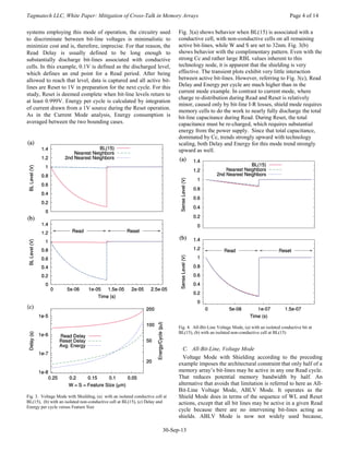
![Tagmatech LLC, White Paper: Mitigation of Cross-Talk in Memory Arrays Page 6 of 14
30-Sep-13
20nm feature size. In a practical situation where a non-zero
sense amp source impedance would add to the effect of series
RBL, the Sense Margin degradation would be greater.
Fig. 6. All-Bit-Line Current Mode, Sense Margin with Time Constraint
IV. CROSS-TALK MITIGATION BY SPATIAL INVERSE
FILTERING
A. The Proposal
What is needed is an operating mode that is more
compatible with the inherent parasitic properties of nano-
meter technology. What is proposed is to characterize cross-
talk effects as signal distortion in the spatial domain and then
devise a spatial filter that compensates for it at the receiving
end of the bit-line signal path. Though not necessarily ideal
mathematically, due to data pattern dependency inherent to the
array, it will be shown that a workable inverse spatial filter
can be formulated for a memory array such as the example of
Fig. 1(b). In effect, a bank of suitably designed sense
amplifiers can function as an inverse spatial filter that de-
convolves cross-talk effects and thereby recovers stored
memory states.
For this exercise, the memory array space has one
dimension, with bit-line array index numbers as the indicator
of spatial position. Inclusion of additional dimensions is
possible, and possibly useful, but this study focuses on a one
dimensional filter function having the following general form:
(1)
where n is the index of a particular bit-line in the model,
VBL(m) is the voltage at the bit-line with index m and K(m-n)
are filter coefficients with index (m-n) that collectively define
the inverse filter characteristic, modulo 32. Filter_Output(n) is
the data state that is ultimately resolved by the filter at bit-line
position, n. Briefly in words, the equation says that the filtered
output associated with a bit-line path in the array is a weighted
sum of all of the bit-line voltages in the array. That can be
complex. Therefore, as a practical matter, it is helpful to zero
out as many of those weighting terms as possible. A way to do
that is shown in the example calculations that follow.
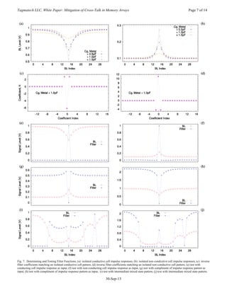
B. Determining a Suitable Filter Function
Undoubtedly there is more than one mathematical method
that might be used to determine the characteristic of the
necessary inverse spatial filter. Purely empirical methods are
conceivable. A genetic algorithm might have advantages.
However, the approach described here is adapted from linear
system theory, using engineering empiricism to achieve the
desired minimization of the filter function and resulting
hardware.
A first step is to generate a spatial impulse response from
the array. That is the specific response that the inverse filter is
designed to match and compensate. Fig. 7(a) and 7(b) each
show responses that may be used for the purpose. They were
extracted from the previously discussed ABLV Mode
simulations for a 32nm memory array. Fig. 7(a) shows array
responses to an isolated conductive cell, with four alternate
values of Cg. Similarly, Fig. 7(b) shows responses to an
isolated non-conductive cell. The choice of conductive cell or
non-conductive cell response is arbitrary at least until actual
hardware is designed, so both are carried through the initial
steps in the example calculation. In practice, the Cg value
should match that expected on the bit-line, including any
loading due to sense amplifier circuitry. For the following
example calculation, the Cg + 1pF characteristics are used. For
this study, the 1pF adder is considered to be allocated as 0.1pF
for sense amplifier loading and 0.9pF due to other elements
such as cell junctions or array segment selection devices that
are not explicitly shown in Fig. 1(b).
A second step is calculation of the coefficients of the
inverse filter. A remarkably efficient tool for that purpose is
Octave [5], an open source, matrix oriented program for
general purpose number crunching. The following one-line
snippet of Octave code accomplishes the transformation of
select impulse response data taken from Fig. 7(a) or 7(b), to
the inverse filter coefficients plotted in Fig. 7(c) or 7(d)
respectively:
inv_imp_resp = shift(ifft((1 ./ fft(imp_in,32)),32),-17)
In the snippet, “imp_in” is a vector containing the bit-line
voltages of the response selected from Fig. 7(a) or 7(b) and
“inv_imp_resp” is a vector containing the resulting inverse
filter coefficients. In words, the snippet finds the Discrete
Fourier Transform (DFT) of the impulse response, calculates
the inverse on an element by element basis, finds the inverse
fourier transform of that, and shifts that to position
coefficients appropriately for use in (1). See the reference [6]
by J.O. Smith, for a concise primer on DFT and convolution
filtering, as well as Octave coding guidance.
In principle, filter coefficient determination could end there
and a circuit could be designed to implement (1) in hardware.
However, consideration of Fig. 7(c) and 7(d) raises the
possibility of a reduction of terms in the equation. In this case,
there are only three coefficients with substantial magnitude.
Only those three adjacent and sharply varying coefficients are
consequential in (1) in terms of filter discrimination between
bit-lines. The others are small and nearly uniform. The small
and nearly uniform coefficients serve only to create an offset
that is related to a rough average of bit-line voltages in a given
pattern. Given that, it seems reasonable to collect those terms
into a single constant OFFSET term and, with algebraic](https://image.slidesharecdn.com/1a483f85-6694-49be-97a6-2a5e8dedc419-161009211542/85/Mitigation-of-Cross-Talk-in-Memory-Arrays-6-320.jpg)
![Tagmatech LLC, White Paper: Mitigation of Cross-Talk in Memory Arrays Page 8 of 14
30-Sep-13
manipulation, reduce (1) to the following form:
(2)
where VBL(n) is the voltage at a bit-line n whose stored state
is to be recovered and VBL(n-1) and VBL(n+1) are voltages at
the bit-lines on either side.
To a very close approximation, since the small uniform
coefficients are near zero in the example cases, GAIN can be
extracted directly from Fig. 7(c) or 7(d) by inspection. GAIN
is approximately the value of K(-1) and K(+1) on the plots.
WEIGHT is then the value of K(0) divided by GAIN.
OFFSET can be derived from (2) by substitution and algebraic
rearrangement. A convenient basis to solve for OFFSET is the
impulse response values for VBL(n-1), VBL(n) and VBL(n+1)
where n is 15, while setting Filter_Out to its ideal output value
when n is 15, which is 1 here.
In a more general case, where the values of the uniform
coefficients K may not be so close to zero and, therefore, may
not be so readily dismissed, it can be useful to make an
adjustment before extracting parameters for (2). The
adjustment is to uniformly translate the K vector contents up
or down in value so as to effectively zero out the nearly
uniform coefficients. That translation has the ultimate effect of
adjusting the GAIN, WEIGHT and OFFSET values to account
for the zeroing of the uniform K values, while preserving the
form of (2). Though not particularly significant in effect here,
that extra step was actually used in the extraction of GAIN,
WEIGHT and OFFSET of the Fig. 7 examples. The resulting
parameter values are listed in Table I.
TABLE I – Filter Parameters
Coefficient
Plot
GAIN WEIGHT OFFSET
Fig. 7(c) 2.81 -2.20 0.558
Fig. 7(d) -4.29 -2.58 -0.241
C. Testing the Filters Numerically
Fig. 7(e) and 7(f) show the result of applying the filters
defined by values in Table I to the impulse response functions
that were first used to determine filter parameters. As
expected, the filter output in each case is a near perfect one
level at the index location of the isolated conductive or non-
conductive cell, with zeros elsewhere. That validates the filter
derivation procedure. Fig. 7(g) and 7(h) then test the
usefulness of the filters by applying them to patterns that are
the opposite of those used in the filter parameter derivation.
Importantly, what is shown is good discrimination between
cell states. However, the restored levels are not ideal. In Fig.
7(g), using the filter matched to an isolated conductive cell,
the filter under-compensates conductive cells that are not
isolated from conductive neighbors. Analogously, in Fig. 7(h),
using the filter matched to an isolated non-conductive bit, non-
conductive cells are over-compensated where they are not
isolated from other non-conductive cells. Though these
bounding cases do fully characterize performance, engineering
intuition may be aided by also looking at filter behavior with a
plausible intermediate pattern. Fig. 7(i) and 7(j) illustrate
behavior given an irregular pattern having conductive cells at
indices 7 through 14, 16 through 21 and at index 26, with non-
conductive cells elsewhere. In Fig. 7(i), compensation for
conductive cells is closest to ideal for the location that is most
isolated, the cell at BL(26). In Fig. 7(j), a similar observation
applies to non-conductive cell locations, such as BL(15).
The observed non-ideal aspect of filter behavior can be
understood by thinking about how stored data is encoded in
the example memory array, and how that encoding must affect
array dynamics. Network dynamics in Fig. 1(b) are R-C in
nature, where the dominant R values in Read mode are
RDATA. Varying the number and locations of coupled
conductive cell RDATA values, as happens in normal memory
data storage operations, inevitably varies the R-C dynamics. A
spatial filter matched to an array with a single conductive or
non-conductive cell will not be a perfect match to an array
having a different physical arrangement of RDATA values.
However, the effect of pattern dependent over or under-
compensation can be masked in filter implementation. The
tendency to under-compensate, as in Fig. 7(g) and 7(i), can be
empirically corrected by proportionately increasing GAIN to
bring the worst case levels in the pattern to a target minimum
level, such as one, and then clamping the other levels at that
level as a maximum. The tendency to over-compensate, as in
Fig. 7(h) and 7(j), requires only clamping at a target
maximum. The important consideration in a digital memory
application is that the spatial filter clearly discriminates
between stored states, as is evident in the last four plots of Fig.
7. Analog level ideality is not required.
V. SPATIAL FILTER IMPLEMENTATION IN HARDWARE
A. Implementation Options
In a semiconductor memory product, it might be possible to
literally evaluate (1) or (2) using a digital processor, after first
converting analog levels to a digital representation. However,
in many applications, the power, chip area or processing delay
associated with such a general approach would be
unacceptable. Because of that, the next segment of this paper
focuses on the feasibility of implementation of (2) in analog
hardware.
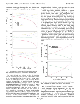
B. A Switched Capacitor Spatial Filter Circuit
1) Technology Independent Circuit Considerations
In a technology agnostic form, Fig. 8(a) shows an example
of a switched capacitor circuit [7] implementation of (2).
Inputs are voltages from a target bit-line at BL, its immediate
neighbors at BL-1 and BL+1, and a voltage level representing
the OFFSET value. The OUT level represents as a voltage the
weighted sum of the inputs, with weights being determined by
ratios of C1 through C4 relative to Cf. Numerical signs of the
weights are determined by switch and capacitor circuit
topology. The specific topology of Fig. 8(a) conforms to the
signs of the parameters of Table I which were derived from
Fig. 7(d). That example and the corresponding 32nm array
model are the basis for the circuit analysis that follows.](https://image.slidesharecdn.com/1a483f85-6694-49be-97a6-2a5e8dedc419-161009211542/85/Mitigation-of-Cross-Talk-in-Memory-Arrays-8-320.jpg)
![Tagmatech LLC, White Paper: Mitigation of Cross-Talk in Memory Arrays Page 9 of 14
30-Sep-13
Fig. 8. Filter Implementation, (a) Switched-Capacitors with ideal Op-Amp,
(b) A practical CMOS circuit with Gain Stage and separate Buffer.
Referring to Fig. 8(a), the Read operation begins with a
sampling phase when bit-lines are connected through switches
to C1 through C3, and C4 is connected to a DC voltage.
During the sampling phase, memory cells discharge bit-lines
at a rate that depends on stored data and those bit-line levels
are mirrored on the capacitors through the switches. The
switches in Fig. 8 are shown in the sampling phase. It is worth
noting that, during that initial phase, the capacitors present to
the bit-lines a capacitance to ground that is in parallel with bit-
line capacitance Cg, which in Fig. 5(c) is shown to be
constructive in terms of signal margin. A second phase of
circuit operation begins after bit-lines have been allowed
sufficient time to develop signals, when the switches flip to
the state opposite of that shown. During the second phase, the
filtered signal develops at OUT.
It is instructive to use the circuit structure of Fig. 8(a) to
assess the essential sensitivity of the filter to variation in
capacitor values. In a switched capacitor circuit, capacitors are
the primary determinant of circuit behavior when amplifier
and switching elements are properly designed. Fig. 9 shows
the result of a monte-carlo analysis of capacitor variation
using Octave. The procedure was to generate 1000
combinations of values for the five capacitors, convert those
back to corresponding filter parameters for (2), calculate filter
output levels using (2) given the bit-line voltages of the
bounding and mixed patterns used previously and, finally,
calculate the mean and standard deviation of filter output at
each bit-line index, for each pattern. For the results in Fig. 9,
individual capacitor variations were uncorrelated and normally
distributed, with 1σ variation set at 1% of nominal values.
Error bars show 3σ variation in filter output levels, which
corresponds to 3% capacitor variation. Importantly, that is a
much larger variation than is considered permissible in many
switched capacitor circuit applications. Despite that, the
remaining Read margin is shown to be substantial. That
suggests capacitors can be much smaller than might be
conventionally assumed, and the remaining performance
tolerance is likely sufficient to also accommodate other
sources of significant variation. As should be expected,
margin defined by the bounding patterns in Fig. 9(a) is very
similar to, and at least as limiting as the margin evident in the
intermediate mixed state pattern of Fig. 9(b).
Fig. 9. Filter Variation due to Capacitor Value Error, (a) with bounding case
patterns overlaid, isolated conducting cell and isolated non-conducting cell,
(b) with an intermediate mixed state pattern.
A further implication of Fig. 9 is that a practical design
procedure may accommodate random variation by means of
empirical adjustments to the GAIN and OFFSET parameters
of (2). Given a target tolerance for capacitor variation, such as
the example of 3% at 3σ, OFFSET can be adjusted in a
negative direction by the indicated “Adj. Offset” amount to
ensure a solid zero output, and GAIN can be increased by a
factor of 1/(“3σ Margin”) to ensure a solid one output, at 3σ.
This and further practical considerations are comprehended in
the following discussion of CMOS circuit implementation.
2) A Filter Circuit in 32nm CMOS PTM Technology
Fig. 8(b) illustrates a switched capacitor circuit with
topology similar to Fig. 8(a), but with a CMOS cascode
amplifier [8] followed by a buffer. The cascode provides high
gain in a compact circuit. A buffer is required because a
cascode stage necessarily has a somewhat limited output
voltage swing and that must be translated to full rail for the
interface to digital logic. It should be noted that inclusion of
the buffer results in an inversion at the OUT node relative to
the circuit of Fig. 8(a). That is unimportant in system design,
but is needed to understand the simulation results that follow.](https://image.slidesharecdn.com/1a483f85-6694-49be-97a6-2a5e8dedc419-161009211542/85/Mitigation-of-Cross-Talk-in-Memory-Arrays-9-320.jpg)
![Tagmatech LLC, White Paper: Mitigation of Cross-Talk in Memory Arrays Page 10 of 14
30-Sep-13
For this design and simulation exercise, “32nm_LP.pm” PTM
CMOS transistor models [3] are used.
In the example circuit, the cascode bias levels are set to
hold the drains of the input transistors at roughly 200mV from
respective power rails. Transistor widths are all 128nm, four
times the minimum feature. Except for the switches, gate
lengths are 64nm. The switches are modeled as full CMOS
transfer gates with 32nm gate lengths. In operation, during the
sampling phase, the cascode is stabilized at its quiescent point
through the switch between its input and output. Typical
quiescent current in the cascode stage is 53nA. With power
supply variation of 1V ± 5% and temperature variation of 0 to
70C, the cascode stage open loop gain always exceeds 200.
That is sufficient for accurate summing, given a closed loop
gain in the rather low range that is required for the filter. That,
combined with capacitive coupling of the SUM node to the
amplifier input gates through Cc, should result in a high
degree of manufacturing process independence. Only the
direct coupling of cascode to buffer presents any requirement
for transistor parameter tracking, but any error there can be
made non-critical with sufficient output swing from the
cascode stage.
In section V.B.1, filter parameter adjustments to
compensate for variation in capacitor values were described.
With the addition of the buffer as shown in Fig. 8(b), further
adjustments can be useful. GAIN can be reduced in proportion
to the reduction in output amplitude required from the gain
stage, with concomitant reduction in cascode amplifier
sensitivity to transistor parameters. OFFSET may be further
adjusted to optimally align gain stage output levels with the
buffer’s input requirements. For this example, overall
adjustments can be summarized mathematically as follows:
(3)
(4)
where GAIN and OFFSET are the unadjusted filter parameters
of (2), BINhigh and BINlow are the input levels to the buffer
stage that are required for reliable full rail levels at OUT,
MChigh and MClow are the monte-carlo analysis results for
worst case (3σ here) high and low level outputs from the
unadjusted filter, Vdd is the power supply voltage that defines
full rail output limits and Qgs is the static operating point of the
GAIN stage. OFFSETemp is useful to account for subtle, non-
ideal circuit behavior. For this exercise, BINhigh is 0.58V,
BINlow is 0.39V, MChigh and MClow are the levels at BL index
15 of Fig. 9(a), Qgs is 0.487V and OFFSETemp is -0.05V and
Vdd is 1V. The resulting parameter adjustments are
summarized in Table II.
The capacitor values in Table III are calculated from Table
II, given a 0.1pF allocation for the total load presented to each
bit-line by sense amplifiers. The architectural assumption is an
all-bit-line type of array where each bit-line is loaded with a
C2 from its own sense amplifier, and both a C1 and a C3 from
immediate neighbors.
TABLE II – Filter Parameter Adjustment for Capacitor
Variation and Output Buffering
Parameter Set GAIN WEIGHT OFFSET
Nominal -4.29 -2.58 -0.241
Adjusted -1.21 -2.58 -0.210
TABLE III – Weighting Capacitor Values (fF)
Capacitor
Values
C1 C2 C3 C4 Cf
Nominal 21.8 56.4 21.8 5.09 5.09
Adjusted 21.8 56.4 21.8 18.0 18.0
Circuit operating margin optimization and parameter
centering was accomplished by means of a 100 run monte-
carlo simulation with capacitor values being varied according
to a normal random distribution, repeated at each of the four
afore mentioned combinations of power supply voltage and
temperature, for each of the bounding pattern cases used
previously in this study. The strategy was to increase the
variance input to the circuit simulation until failures could be
seen and then use that to adjust for any asymmetry in behavior
with respect to stored state or environmental variables.
Centering correction was implemented by adjusting
OFFSETemp. As anecdotal evidence of circuit robustness, it is
interesting to note that a 10% uncorrelated capacitor variation
at 3σ produced no failures in any of the four 100 run monte-
carlo simulations, given the final adjusted values of Table II
and Table III, with a 0.05V OFFSETemp value. Lacking skew
versions of the PTM 32nm_LP transistor models, transistor
parameter variation was not included in the variation analysis.
However, with the switched-capacitor approach mitigating any
transistor threshold variation effects, with open loop gain
being more than two orders of magnitude greater than closed
loop, and with sufficient drive levels provided to the buffer
stage to guarantee switching, transistor parameter variation
should not have an important impact on functional failure rate.
Fig. 10 shows an example of behavior of the circuit with
adjusted parameters, with the 32 bit array model of Fig. 1(b),
where W and S are set at 32nm. The sampling phase is shown
ending at approximately 1.29µs. Prior to that time, FBK is at
its quiescent level. Immediately after, FBK begins reacting.
FBK rises when reading a non-conducting cell such as at
BL(15) in Fig. 10(a) and falls when reading a conducting cell
such as at BL(26) in Fig. 10(b). FBK moves toward the target
levels deemed necessary to reliably drive the buffer, though
typically the buffer switches sooner, as it does in this case.
The SUM node voltage varies only slightly, functioning as a
virtual ground in the gain stage feedback network. Fig. 10(c)
shows all states reading out correctly despite what would be a
negative signal margin in the context of a conventional voltage
sensing read-out circuit, as in the ABLV mode of section
III.C. In particular, cell states at BL(15) and BL(26) would not
be sensed correctly with ABLV mode, in 32nm technology.](https://image.slidesharecdn.com/1a483f85-6694-49be-97a6-2a5e8dedc419-161009211542/85/Mitigation-of-Cross-Talk-in-Memory-Arrays-10-320.jpg)
![Tagmatech LLC, White Paper: Mitigation of Cross-Talk in Memory Arrays Page 13 of 14
30-Sep-13
be coded as a difference between RDATA values of a bit-line,
BL(n), and an immediate neighbor, BL(n-1). A key point is
that differential operation does not alter the spatial impulse
response of individual bit-lines as compared to single-ended
operation. Consequently, the inverse spatial filter calculation
for differential mode can still be done with respect to
individual bit-lines in a manner identical to the foregoing
single-ended example, yielding the identical result, as
described in (2). To then obtain a filter equation for a
differential pair, (2) may be applied twice, taking the
difference between bit-lines of a pair, as in (5):
(5)
By substitution and algebraic reduction, that becomes:
(6)
Note the filter OFFSET constant of (2) disappears, due to
algebraic cancellation. The result is an equation that is the
weighted sum of four inputs, similar to the single-ended
example, but with one more bit-line input and without the
OFFSET constant. That suggests a circuit implementation
similar to Fig. 8 may be workable after appropriately adjusting
inputs, filter weights and signs. However, in practice, it might
still be useful to include an OFFSET-like term if only for fine
tuning of practical circuitry.
VIII. SUMMARY DISCUSSION
A. Potential Applications
The demonstrated read-out speed and power performance is
in a range compatible with many memory product
specifications. Alternate, advantageous implementations of the
active circuitry may also be possible, especially where higher
supply voltages are available. For the example 32nm CMOS
circuit, current drain per output data bit is low and in a range
compatible with products where simultaneous read-out of a
wide page is necessary, such as NAND Flash memory.
Given the high packing density of NAND arrays, and the
small signal margins inherent with multi-level cell operation,
cancellation of coupling error is likely to be useful to enhance
operating margins. It may prove vital to maintain performance
as scaling progresses below 100nm where even best case
current mode operating margins tends to degrade with scaling.
A further extension in the NAND flash context would be the
use of inverse filtering to compensate word-line oriented
interactions [9], [10]. Rather than sampling bit-line levels
during only a single word-line selection as in the foregoing
example, bit-line signals could also be sampled during the
selection of each of a series of adjacent word-lines, with
simultaneous weighting and summing in a single filter circuit,
thereby compensating word-line oriented causes of cross-talk,
with or without simultaneous compensation of bit-line
oriented cross-talk. The practical limitation would be the
number of terms in the filter equation and the resulting size of
the circuit.
Inverse spatial filtering may be valuable in NOR Flash or
other products that are based on single-ended conductive cells
[11] where higher speeds than NAND may be required. It is
conceivable this may be useful for some varieties of SRAM,
particularly single-ended SRAM [12] where differential
sensing is not the natural design choice and where cell pitches
and bit-line lengths could ultimately be pushed far enough to
cause strong bit-line to bit-line interaction.
Since differential mode is also theoretically supportable,
application to inherently differential memory types is not out
of the question. Conceivable motivations for a differential
implementation might be improved performance due to better
signal energy utilization, avoidance of the cost of the physical
features associated with alternate approaches [1], [2] or the
ability to compensate for interactions too complex for those
other methods of cross-talk mitigation. Though the circuit
example in this study may not be directly applicable to
DRAM, due to the capacitive load it adds to bit-lines,
workable circuit variations are conceivable. For example, a
MOS source follower could be inserted as buffer between the
bit-line and sense amplifier capacitance. It is also conceivable
that, with diligence in modeling weighting capacitors and
lithography in nano-meter technologies, bit-line loading by a
switched-capacitor circuit might be scaled down sufficiently to
be directly compatible with DRAM sensing, without the
addition of input buffers.
B. Suggested Further Work
Key to any application will be optimal implementation in
hardware. Taking the example circuit of this study as a
prototype, it would be useful to study ways to optimize
weighting capacitor packing density, given properties of nano-
meter lithographic processes. The goal is to implement small
capacitors having adequate, but not necessarily precise ratio
accuracy, that are also physically matched to a memory array
bit-line pitch, or some low multiple thereof.
Consideration could also be given to alternate ways to
implement (2) in circuitry. The switched-capacitor example
seems attractive, particularly in single-ended architectures in
MOS memories where the added Cg from the sense circuitry
is actually constructive. However, that should not close off
consideration of static circuit approaches. In some
applications, it may even make sense to use a brute force
digital implementation of the spatial filter calculation. In those
cases, a key will be efficient analog to digital conversion of
bit-line signals.
ACKNOWLEDGMENT
The author would like to thank friends and colleagues who
made numerous helpful suggestions during preparation of this
paper.](https://image.slidesharecdn.com/1a483f85-6694-49be-97a6-2a5e8dedc419-161009211542/85/Mitigation-of-Cross-Talk-in-Memory-Arrays-13-320.jpg)
![Tagmatech LLC, White Paper: Mitigation of Cross-Talk in Memory Arrays Page 14 of 14
30-Sep-13
REFERENCES
[1] Hideto Hidaka, Kazuyasu Fujishima, Yoshio Matsuda, Mikio Asakura,
Tsutomu Yoshihara, “Twisted Bit-Line Architectures for Multi-Megabit
DRAM’s,” IEEE Journal of Solid State Circuits, Vol. 24, pp. 21-27,
February 1989
[2] Dong-Sun Min, Dietrich W. Langer, “Multiple Twisted Dataline
Techniques for Multigigabit DRAM’s,” IEEE Journal of Solid State
Circuits, Vol.34, pp. 856-865, June 1999
[3] Yu(Kevin) Cao, Predictive Technology Model, Arizona State
University, online, available: http://ptm.asu.edu/, Copyright 2007
[4] S.-C. Wong, G.-Y. Lee, D.-J. Ma, “Modeling of Interconnect
Capacitance, Delay, and Crosstalk in VLSI,” IEEE Transactions on
Semiconductor Manufacturing, vol. 13, no. 1, pp. 108-111, February
2000
[5] John W. Eaton, Octave Documentation, online, available:
http://www.gnu.org/software/octave/docs.html, Copyright 1998-2011
[6] J.O. Smith, Mathematics of the Discrete Fourier Transform (DFT) with
Audio Applications, Second Edition, online book, available:
https://ccrma.stanford.edu/~jos/sasp/Convolution_Short_Signals.html,
2007, accessed 15 February 2011.
[7] R. Jacob Baker, Harry W. Li, David E. Boyce, in CMOS Design,
Layout, and Simulation, New York, IEEE Press, 1998, pp. 731-738
[8] David A. Johns, Ken Martin, Analog Integrated Circuit Design, New
York, John Wiley & Sons, Inc, 1997, pp. 137-142
[9] Jae-Duk Lee, Sung-Hoi Hur, Jung-Dal Choi, “Effects of Floating-Gate
Interference on NAND Flash Memory Cell Operation,” IEEE Electron
Device Letters, Vol. 23, pp. 264-266, May 2002
[10] Mincheol Park, Keonsoo Kim, Jong-Ho Park, Jeong-Hyuck Choi,
“Direct Field Effect of Neighboring Cell Transistor on Cell-to-Cell
Interference of NAND Flash Cell Arrays,” IEEE Electron Device
Letters, Vol. 30, pp. 174-177, February 2009
[11] Anant Singh, Michael Ciraula, Don Weiss, John Wuu, Philippe Bauser,
Paul de Champs, Hamid Daghighian, David Fisch, Philippe Graber,
Michel Bron, “A 2ns-Read_latency 4Mb Embedded Floating-Body
Memory Macro in 45nm Technology,” in Solid-State Circuits
Conference-Digest of Technical Papers, San Francisco, 2009, pp. 459-
461
[12] Leland Chang, Yutaka Nakamura, Robert K. Montoye, Jun Sawada,
Andrew K. Martin, Kiyofumi Kinoshita, Fadi H. Gebara, Kanak B.
Agarwal, Dhruva J. Acharyya, Wilfried Haensch, Kohja Hosokawa,
Damir Jamsek, “A 5.3GHz 8T-SRAM with Operation Down to 0.41V in
65nm CMOS,” in Symposium on VLSI Circuits Digest of Technical
Papers, 2007, pp. 252-253
Bruce L. Morton received the B.S. in electrical
engineering from Oklahoma State University in
Stillwater, Oklahoma in 1975. With support of an
Engineering Foundation Fellowship, he earned an M.S.
in electrical engineering from the University of Texas at
Austin, Texas in 1976.
After graduation, he joined Motorola in Austin where
he learned the basics of early MOS technology and
memory design, ultimately contributing to the design of
DRAM, SRAM and Non-Volatile memory for
commodity markets and proprietary System-on-Chip products. In 2005, he
joined AMD/Spansion, working primarily on modeling of developmental
memory devices, circuits and architectures. Being semi-retired since 2009, he
has worked independently on new design ideas, while also consulting on an
occasional basis on the topics of circuit design, devices and technology. In
2012, he formed Tagmatech LLC to continue to develop and license new IP.](https://image.slidesharecdn.com/1a483f85-6694-49be-97a6-2a5e8dedc419-161009211542/85/Mitigation-of-Cross-Talk-in-Memory-Arrays-14-320.jpg)