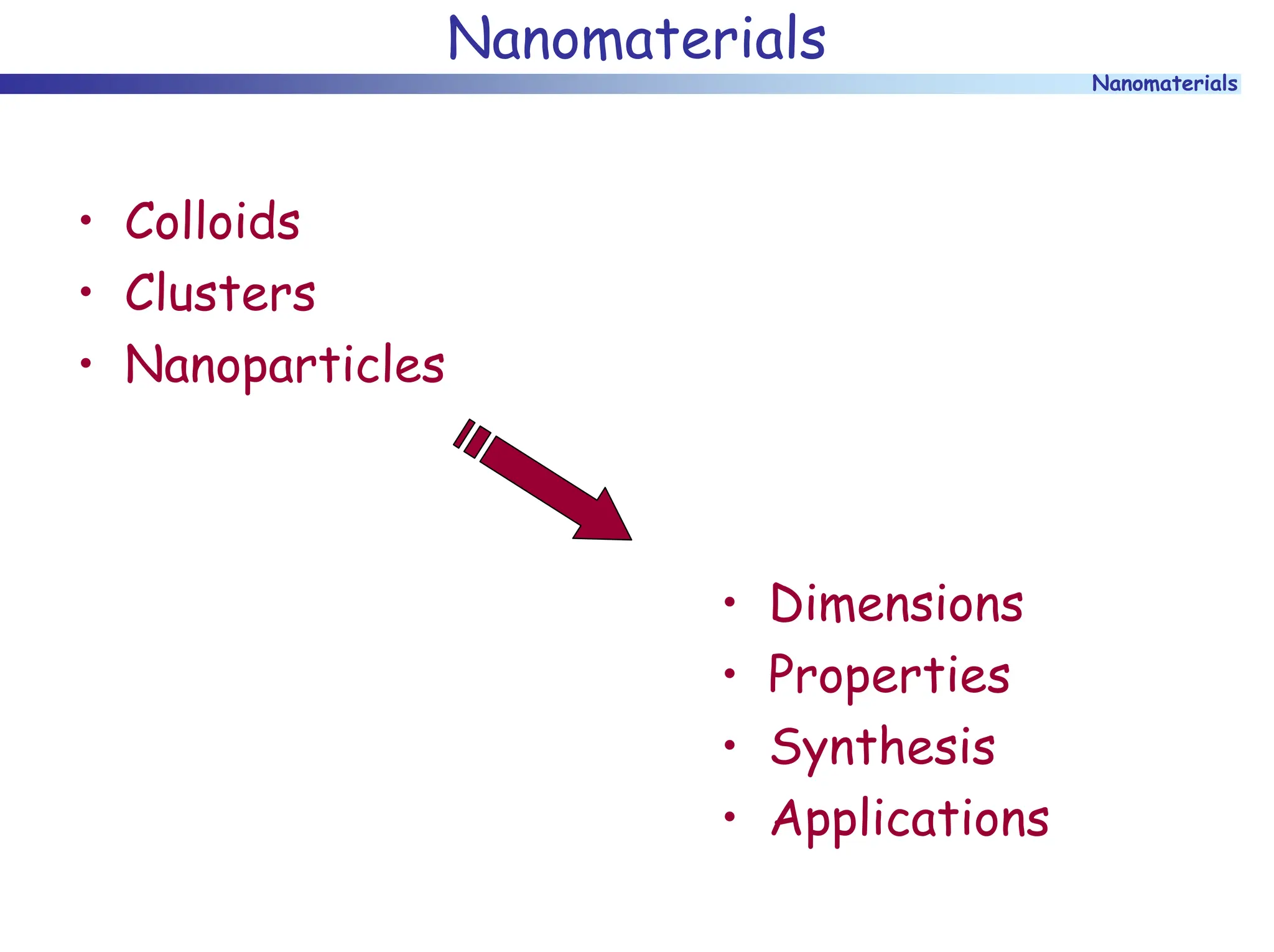
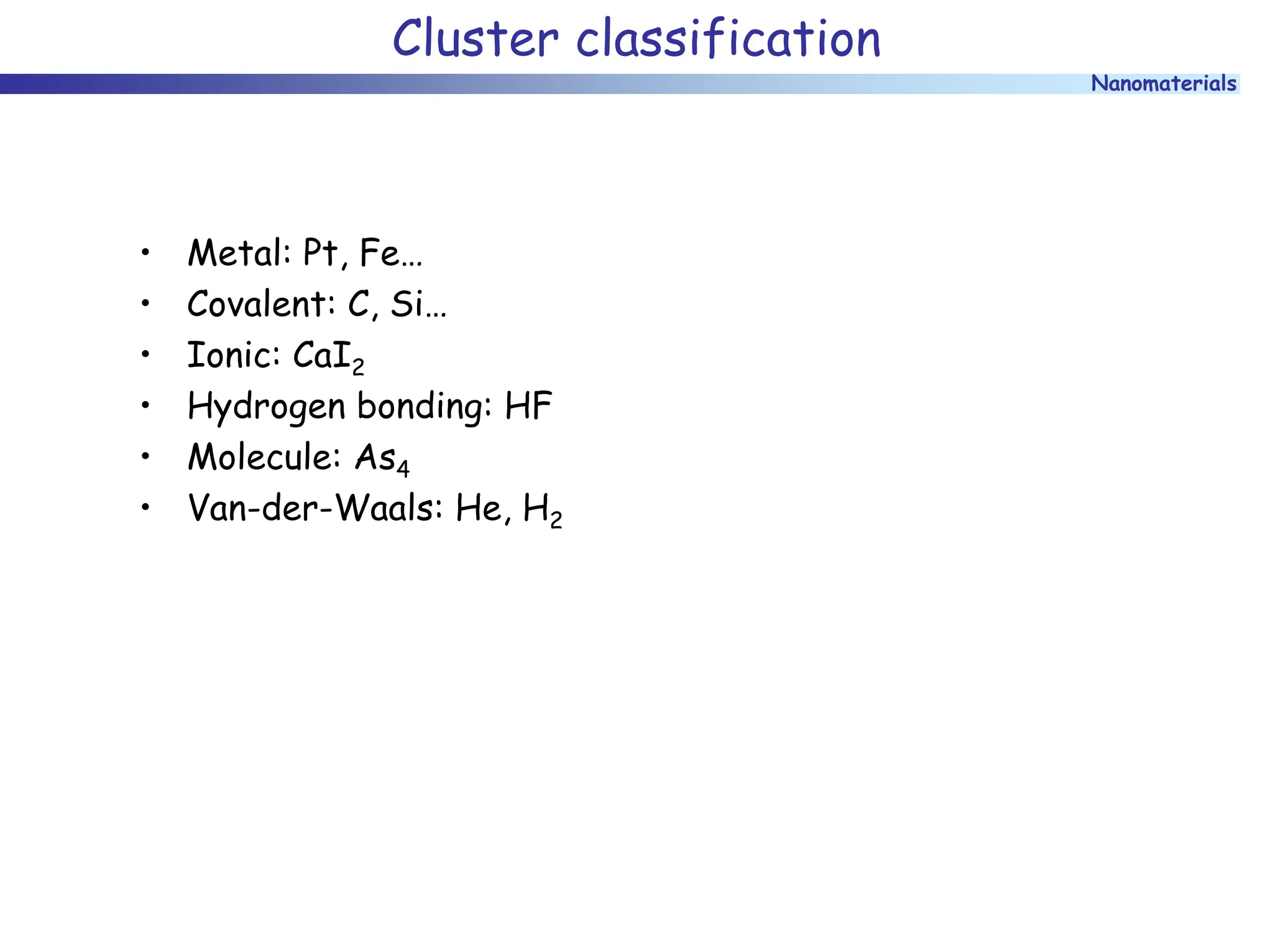
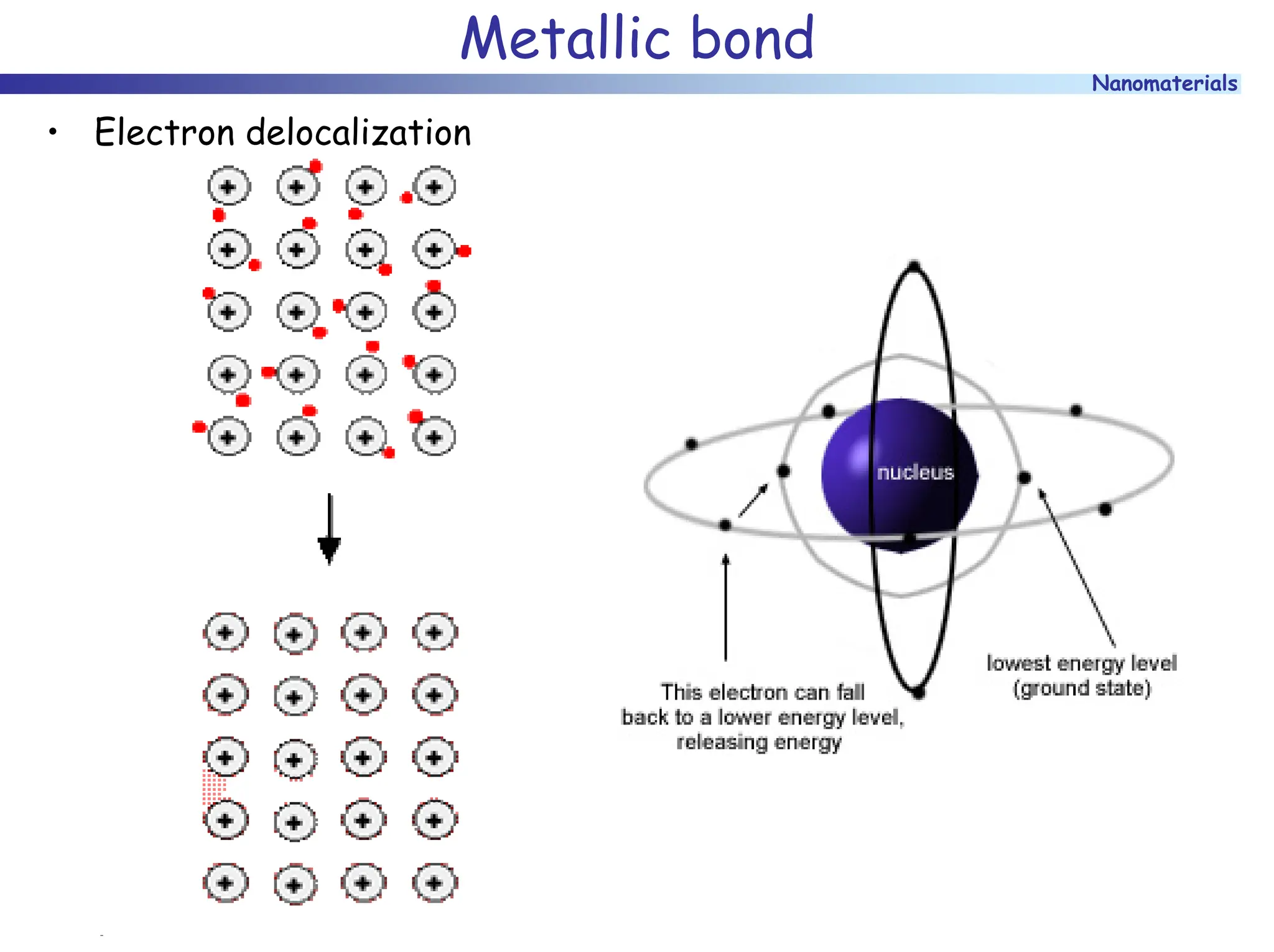
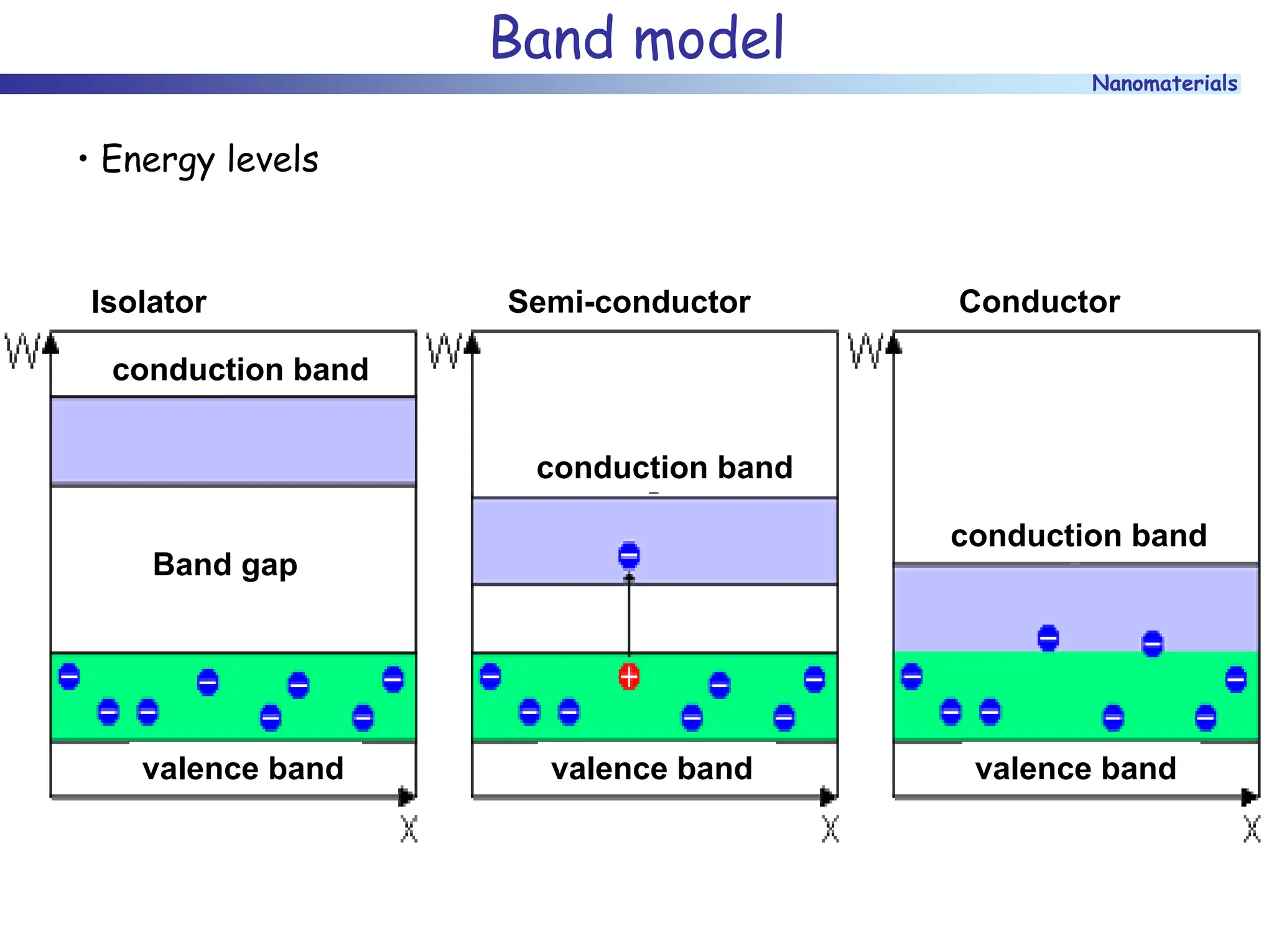
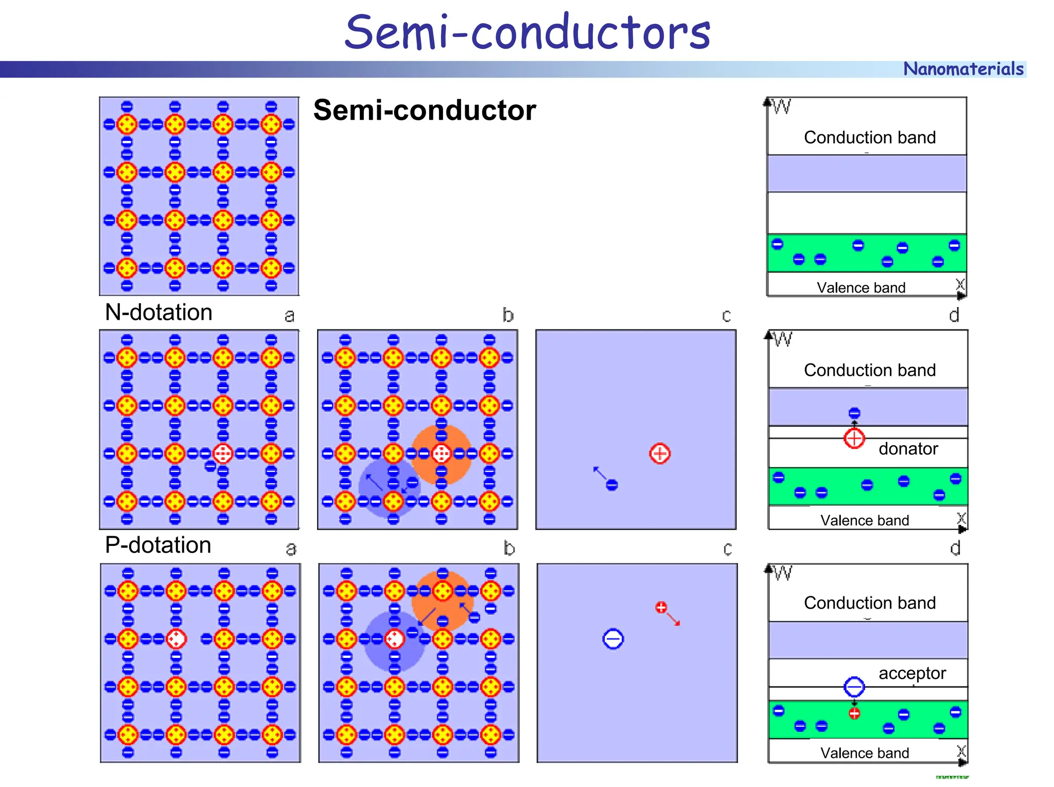
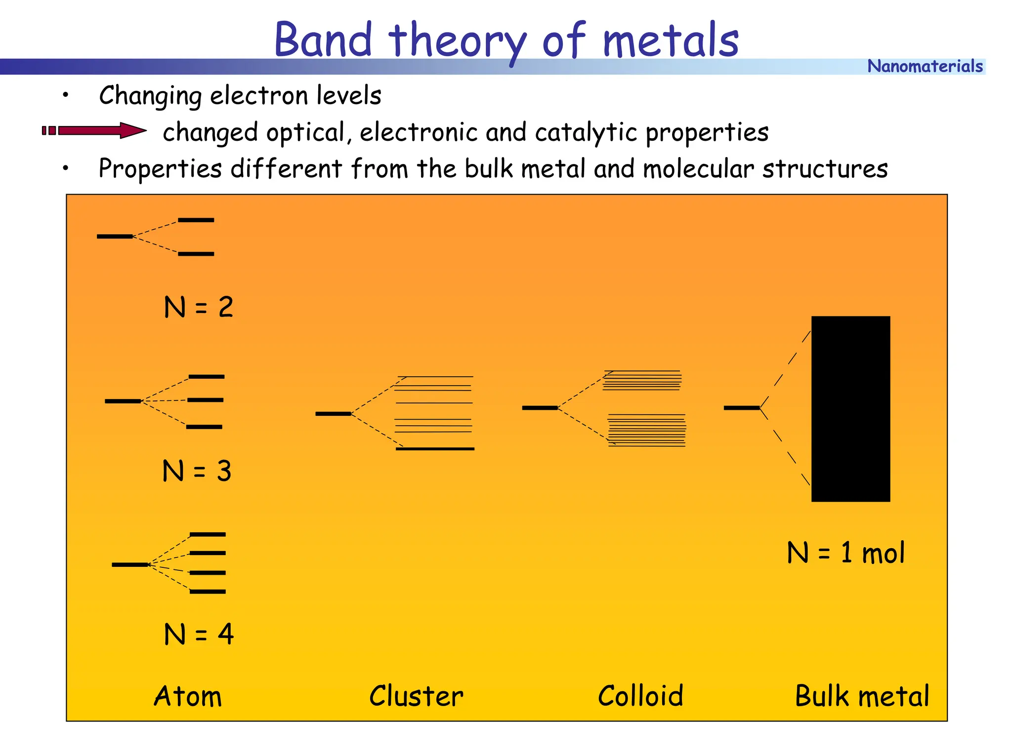
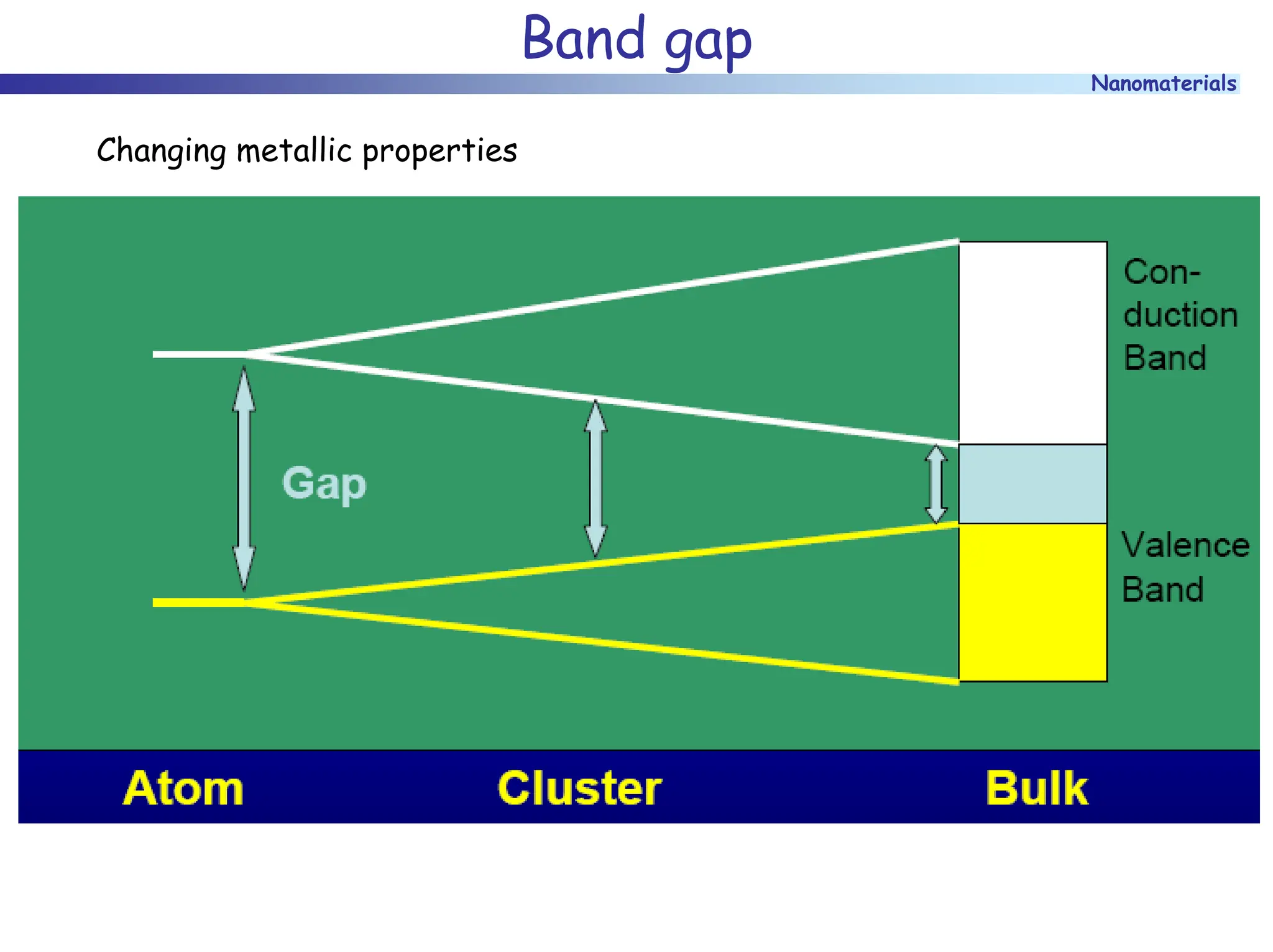
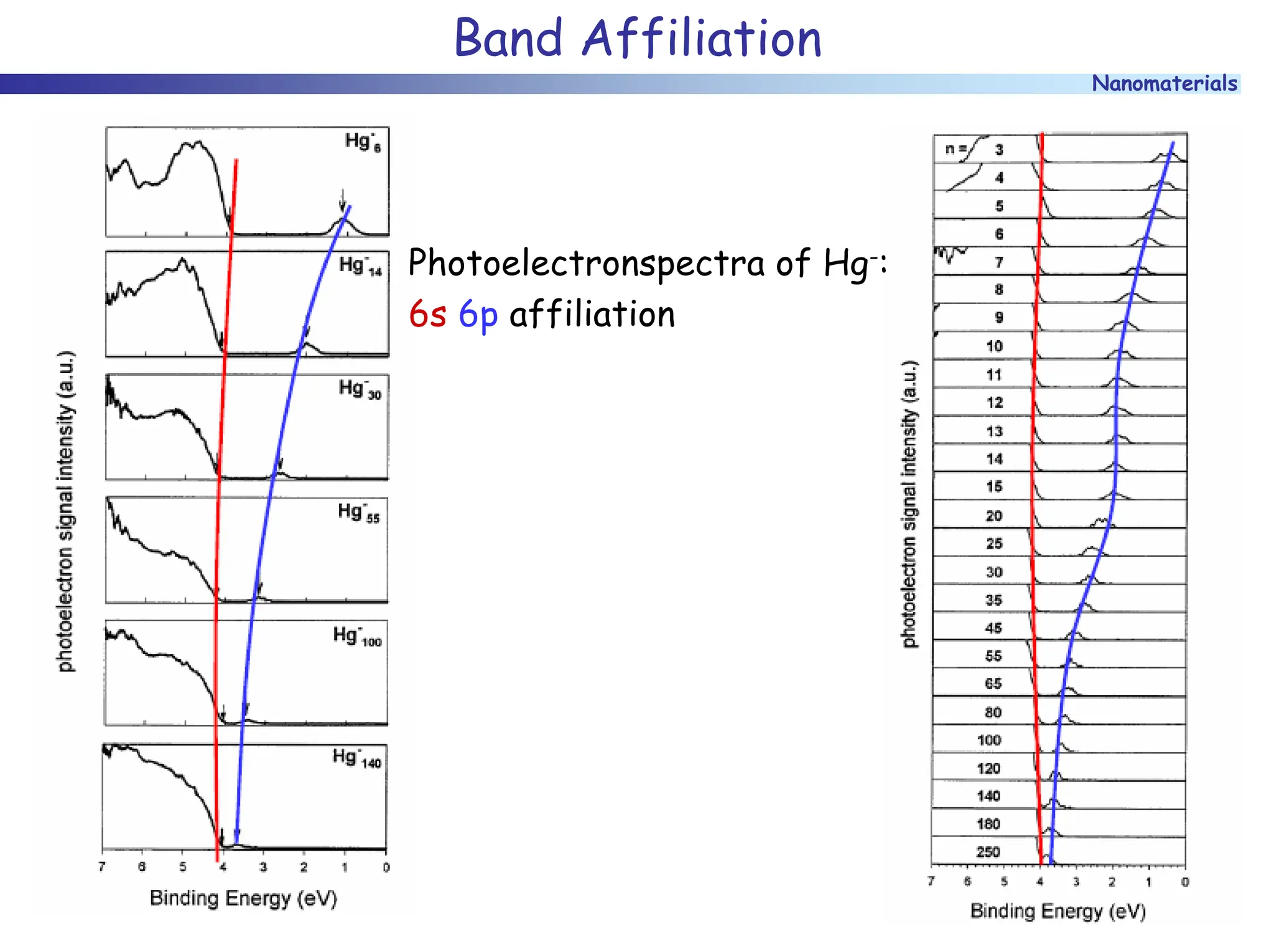
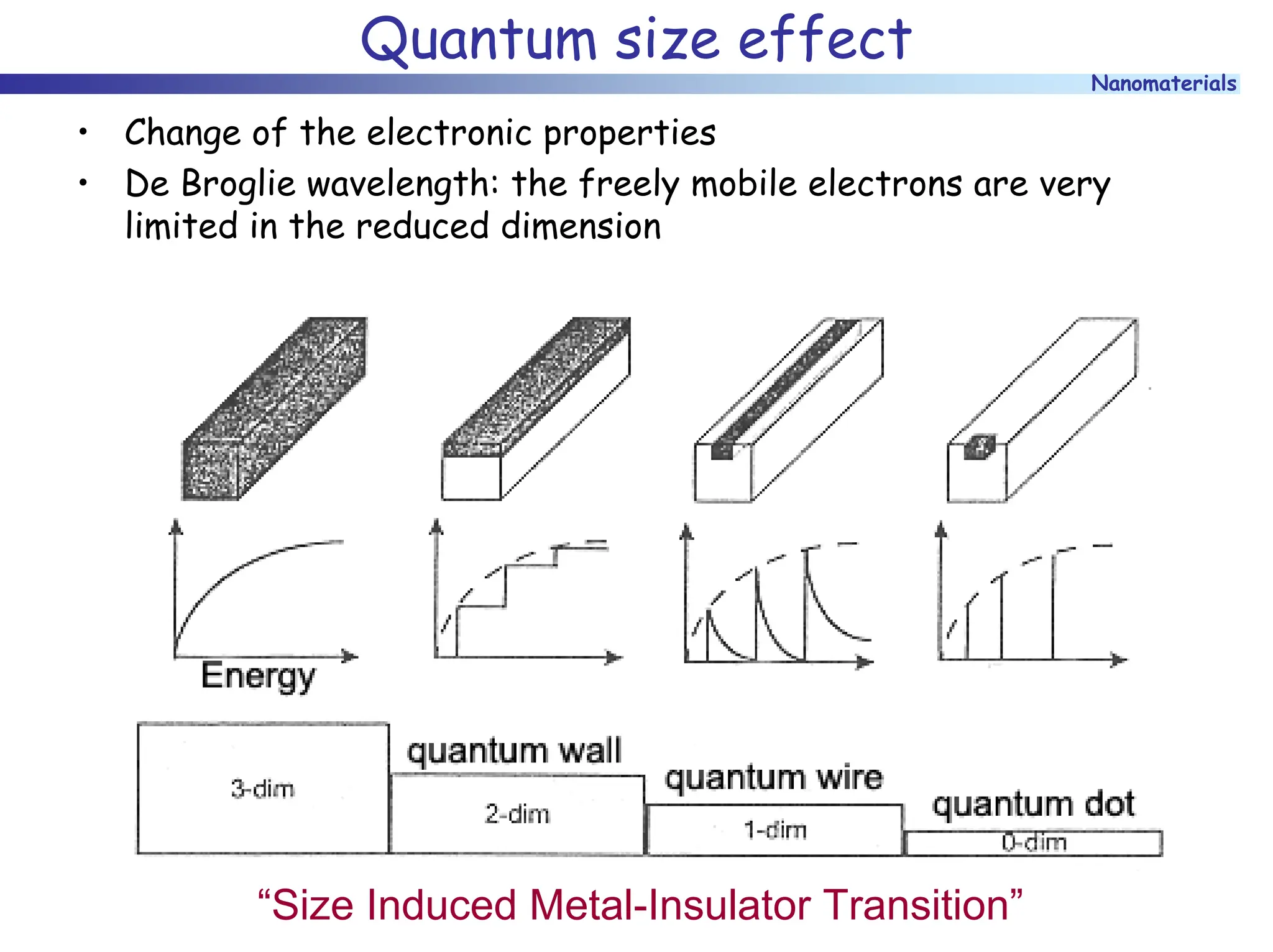
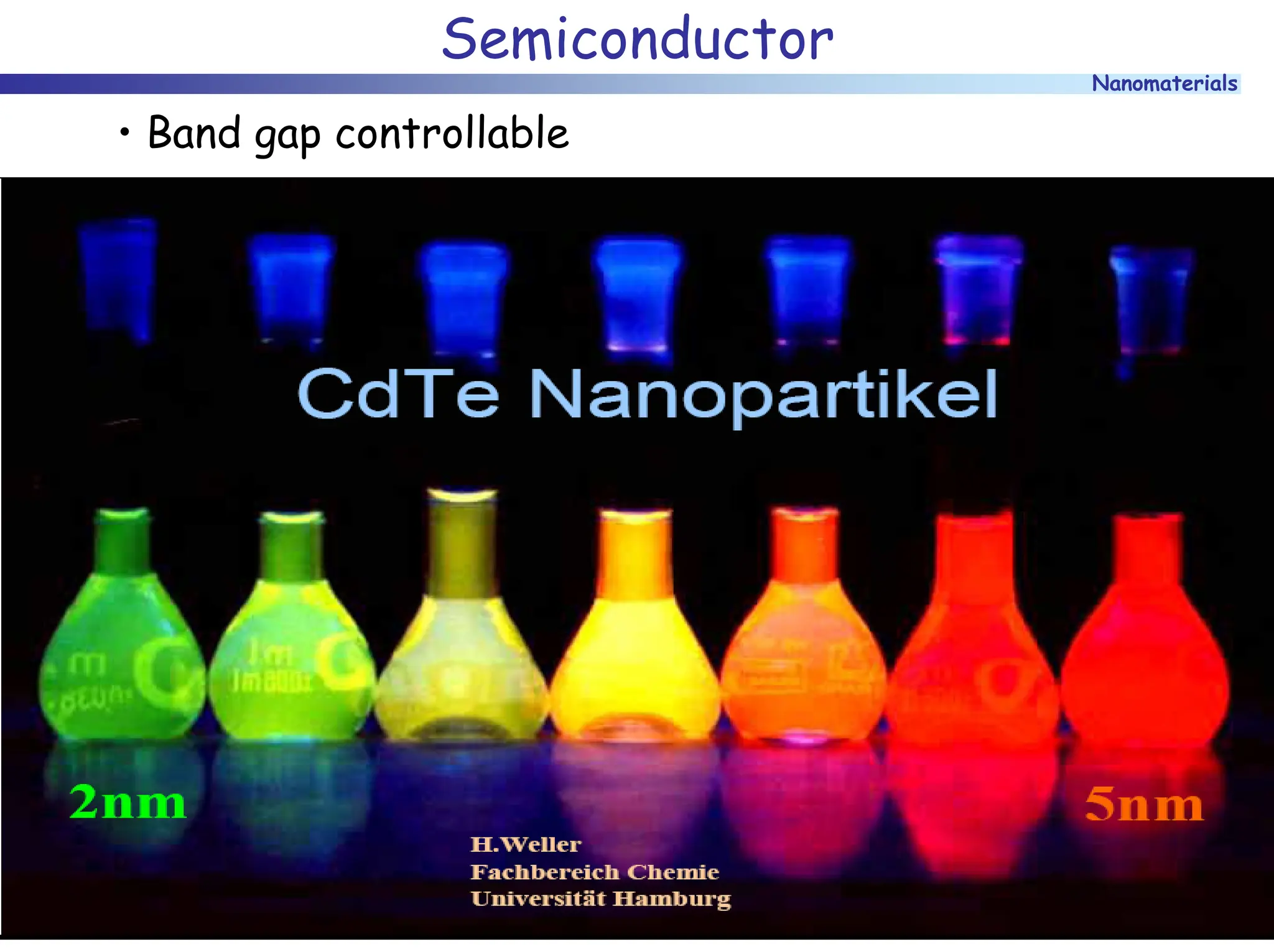
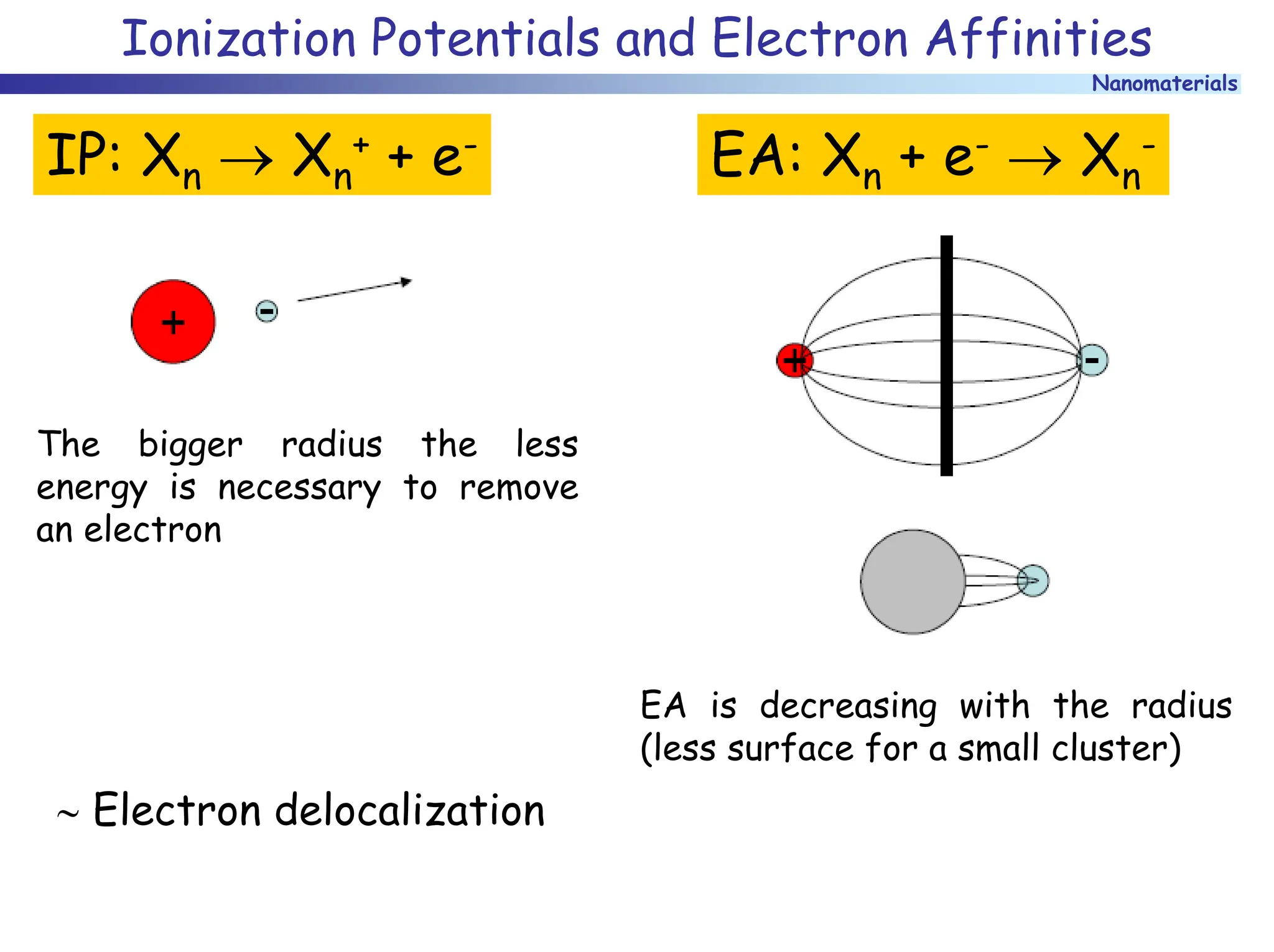
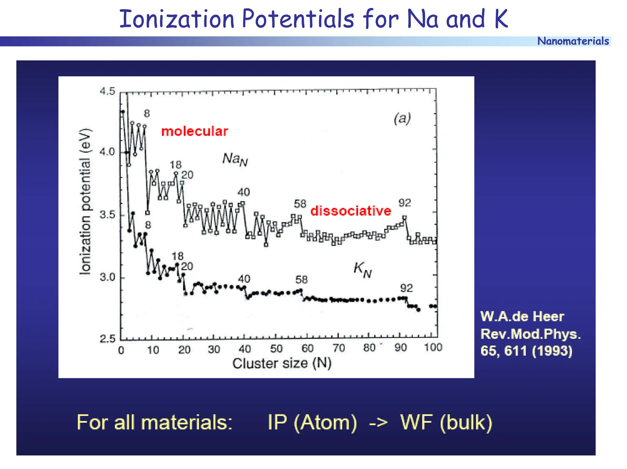
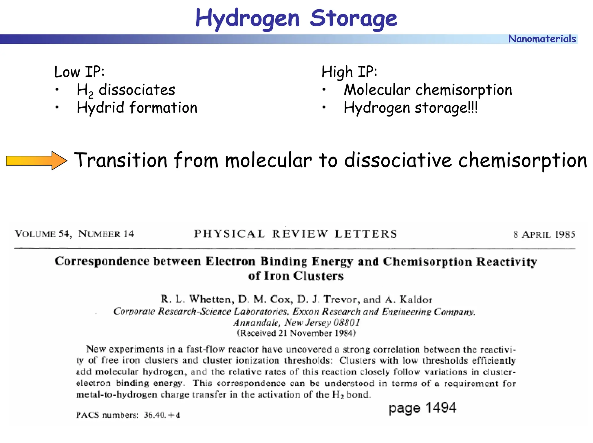
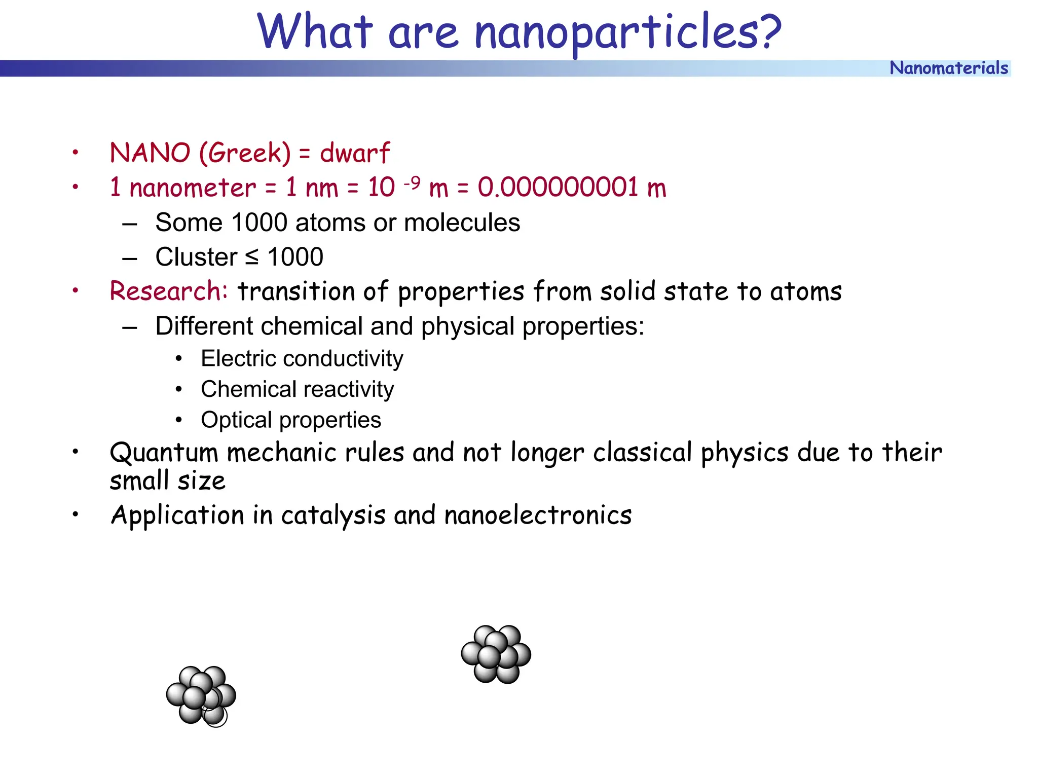
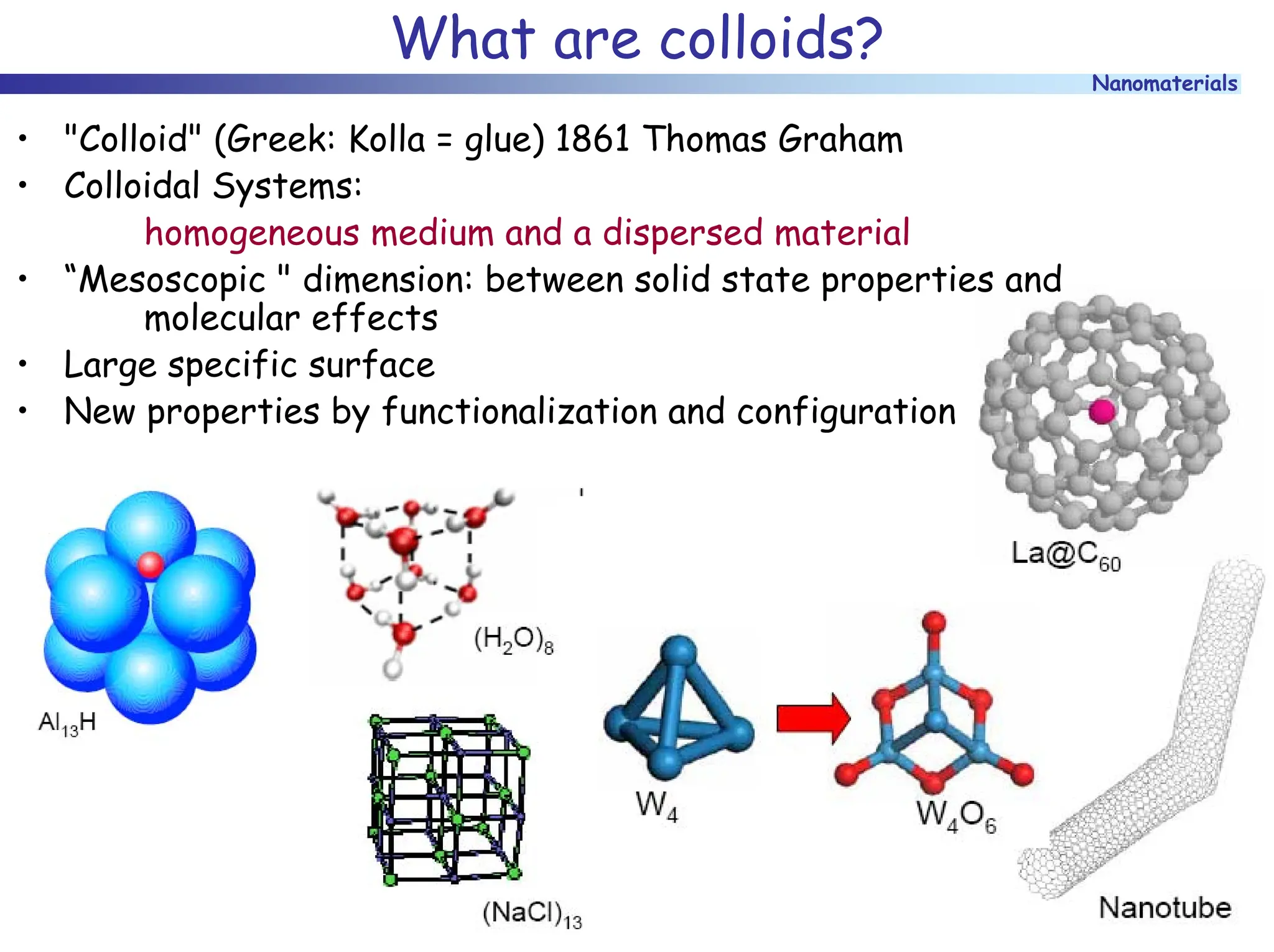
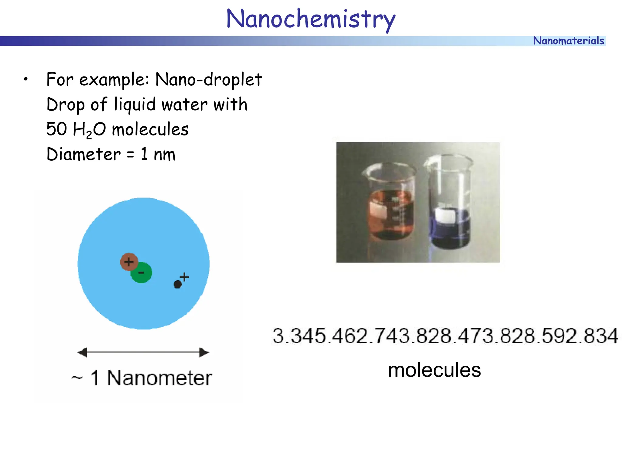
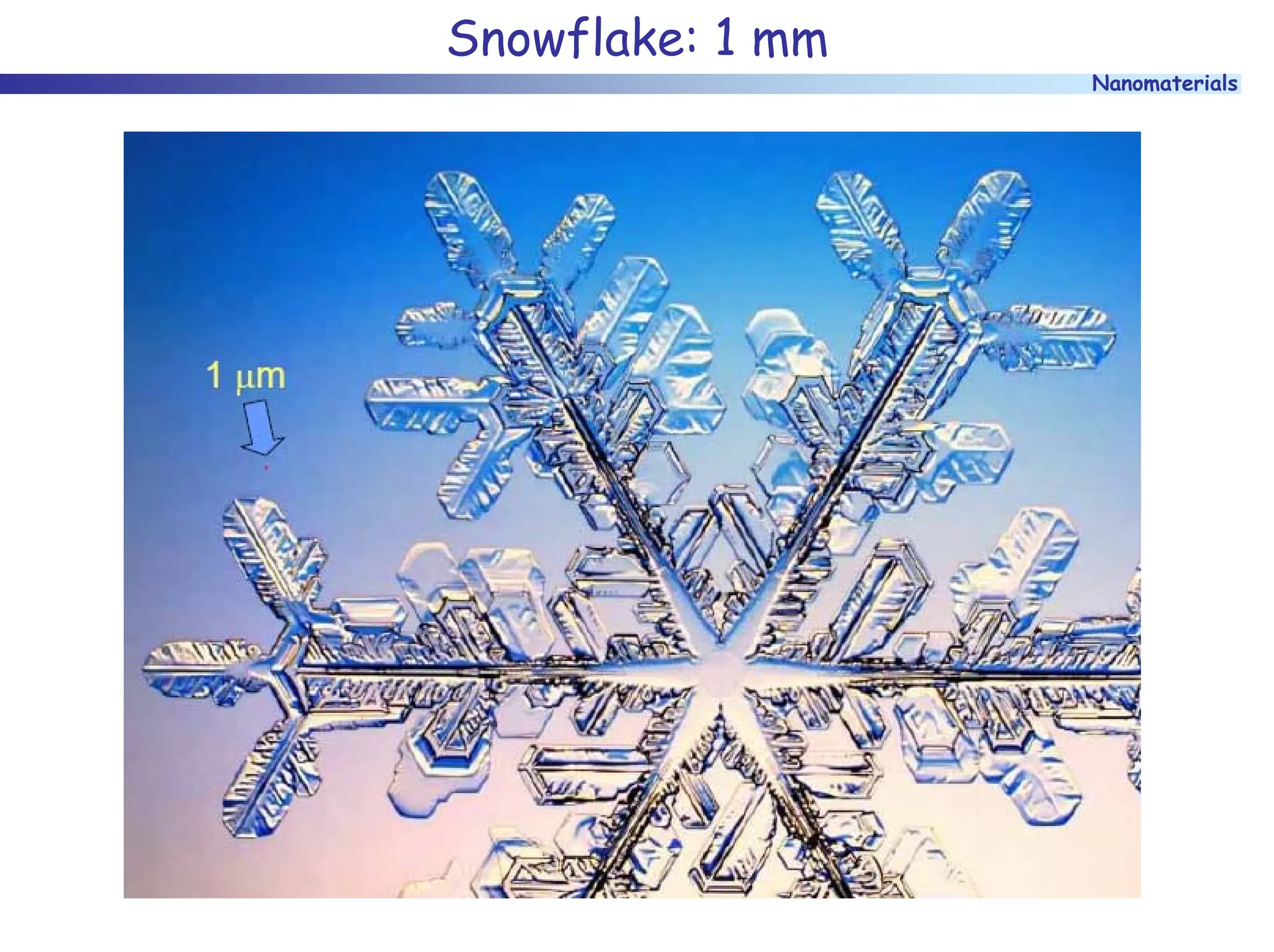
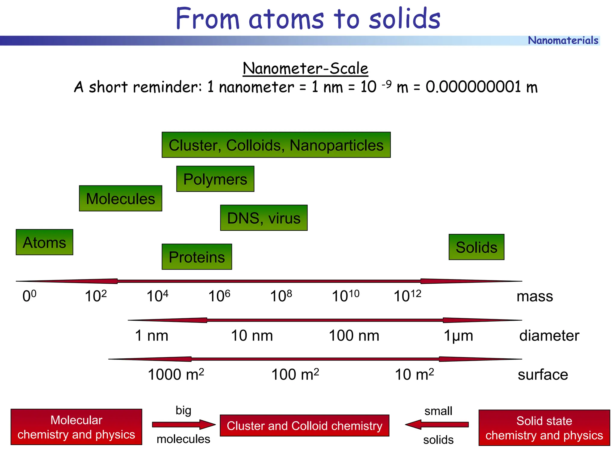
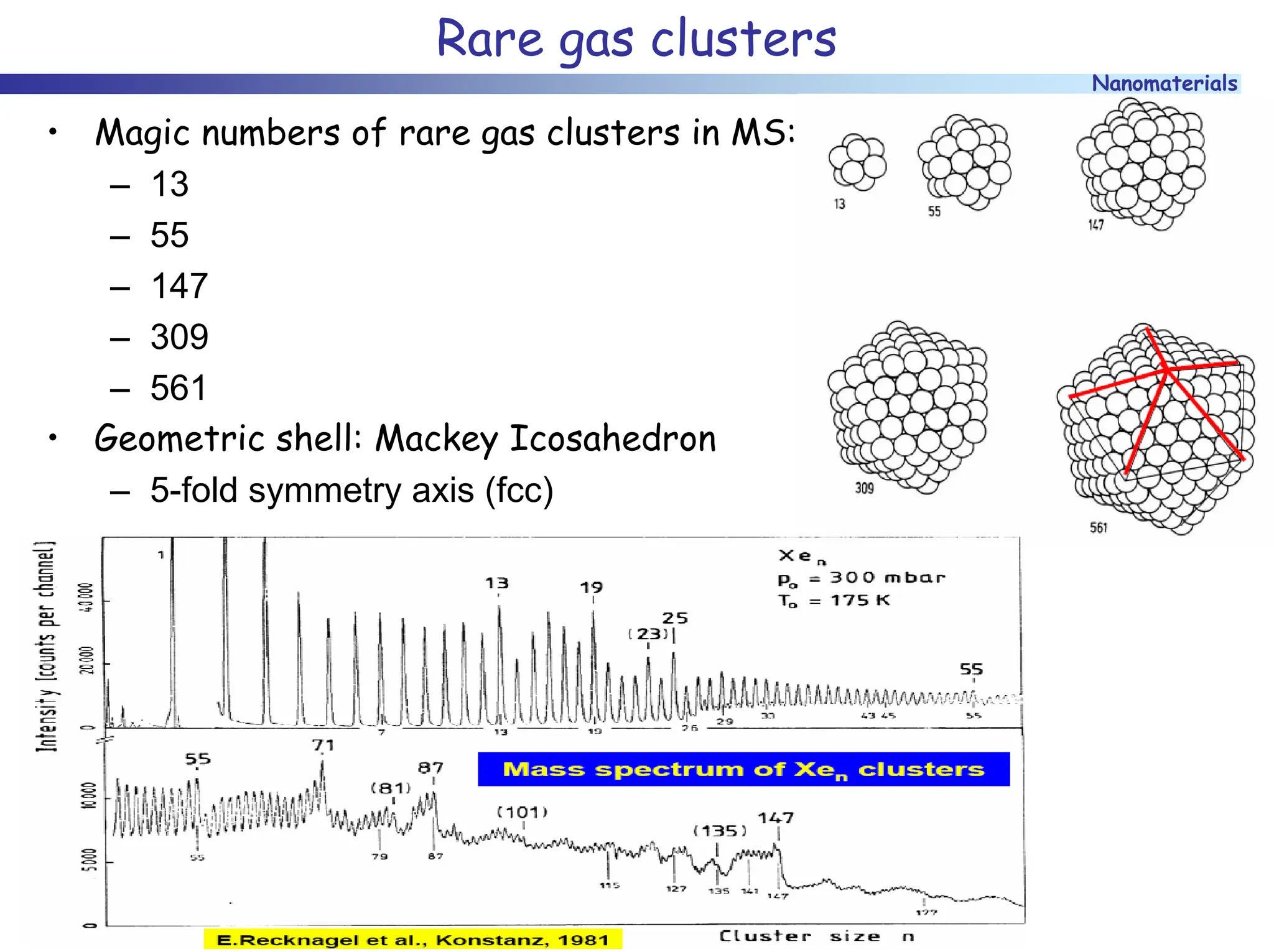
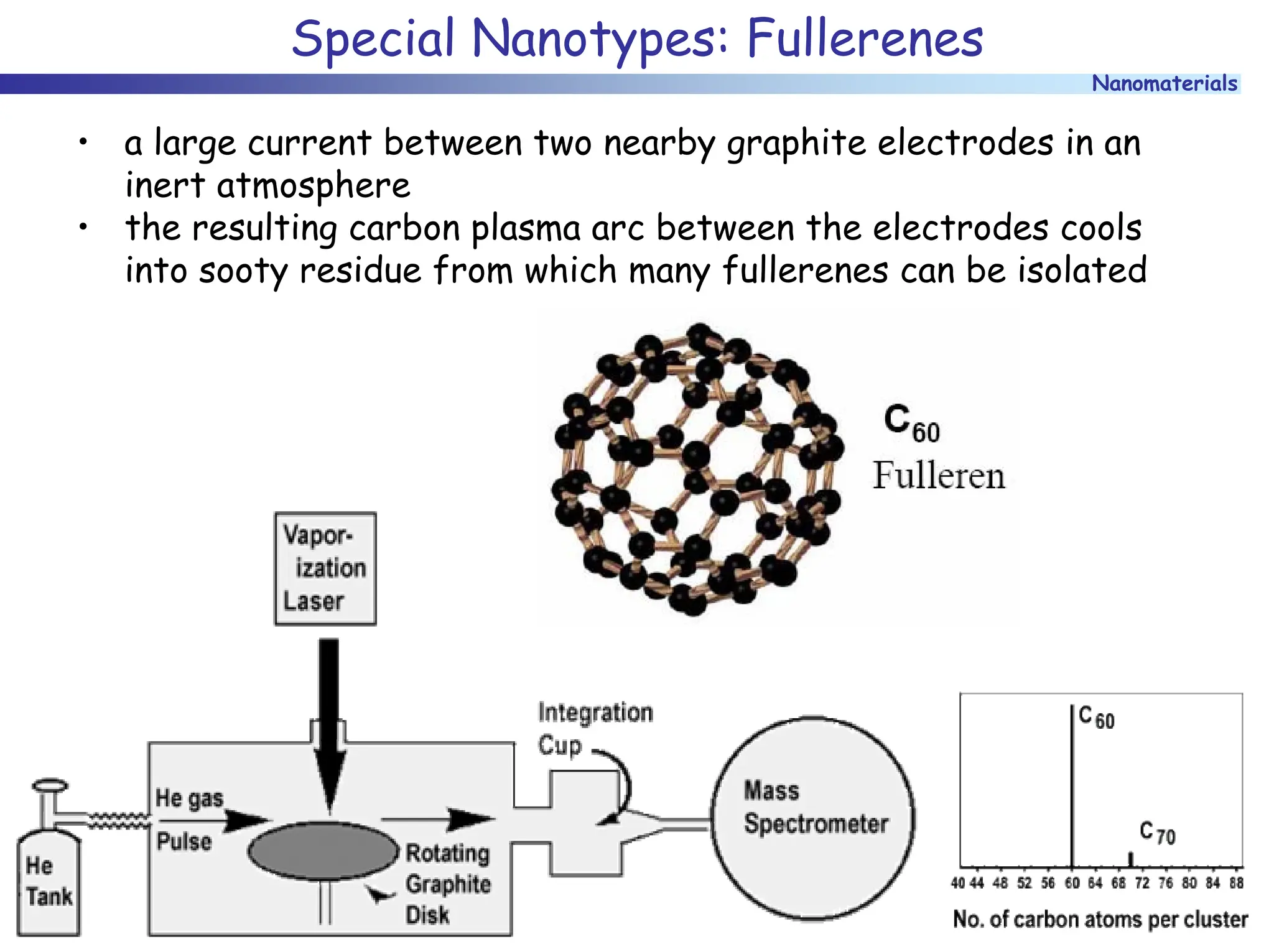
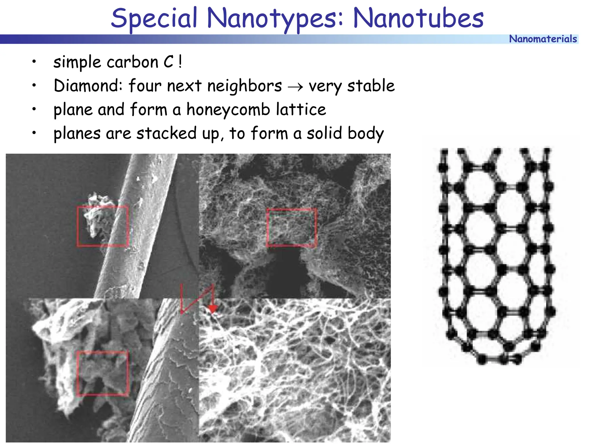
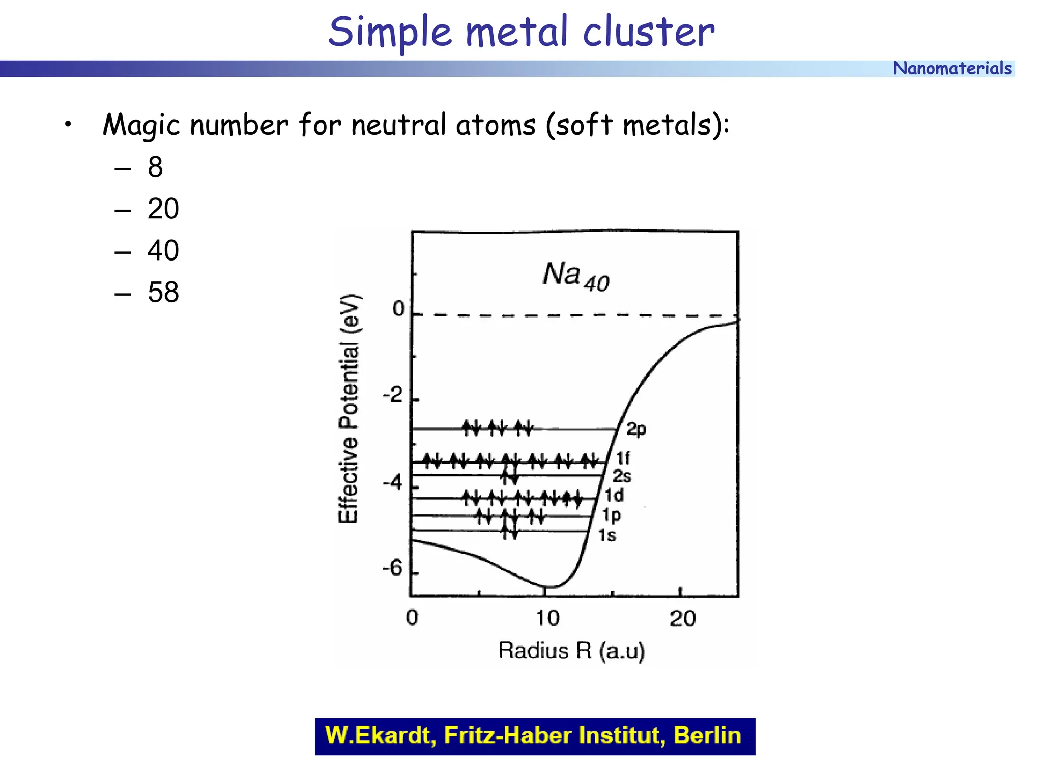
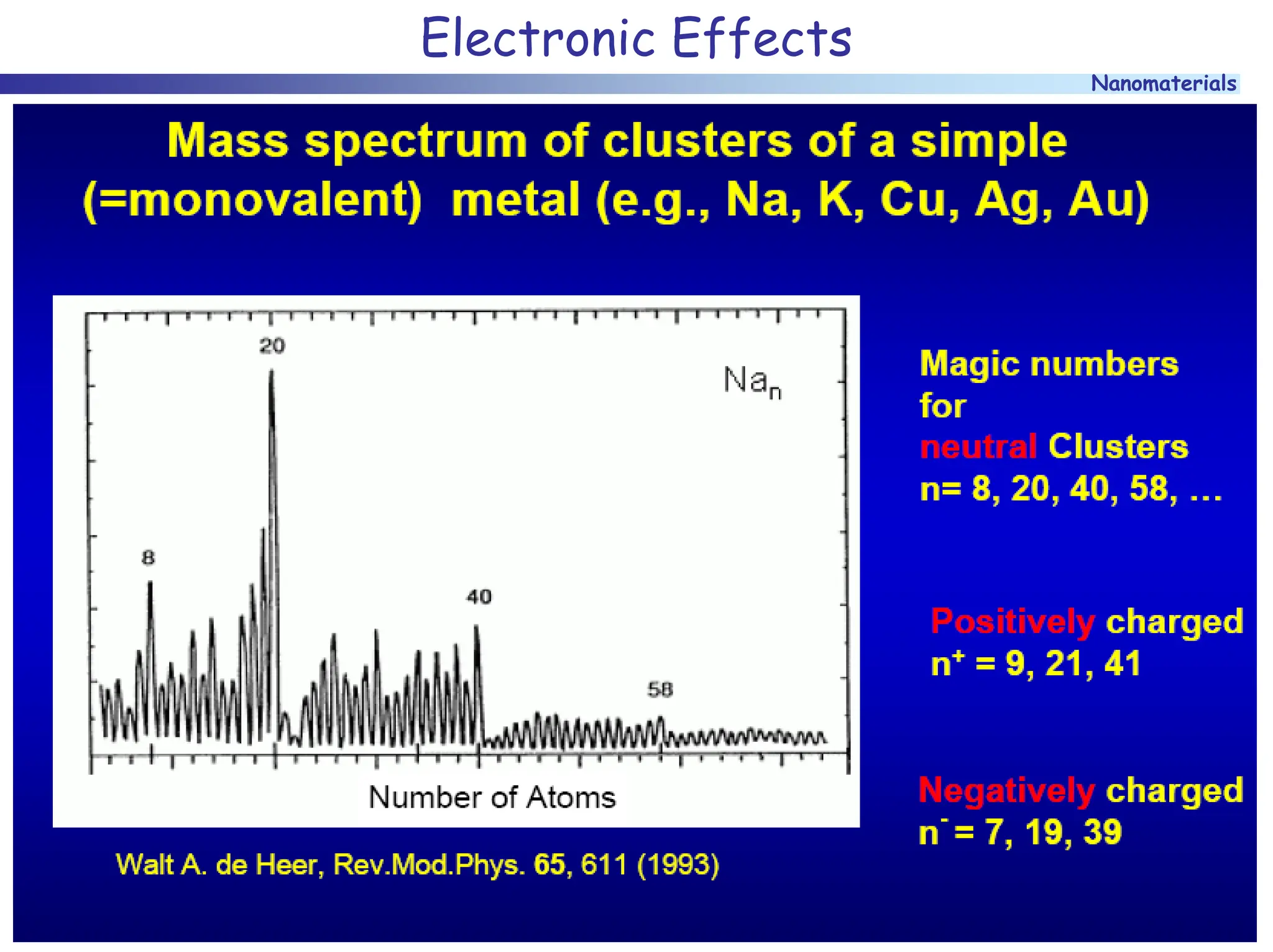
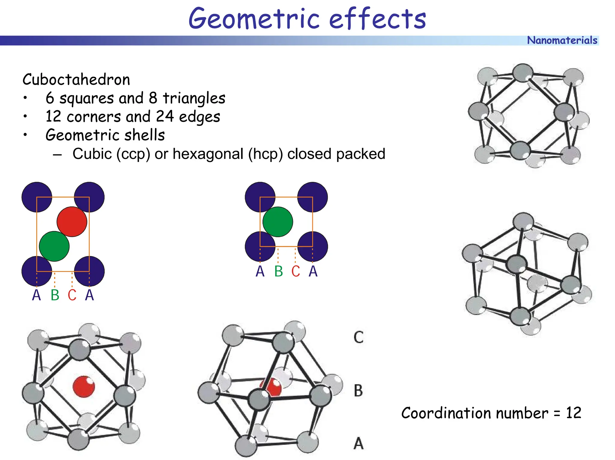
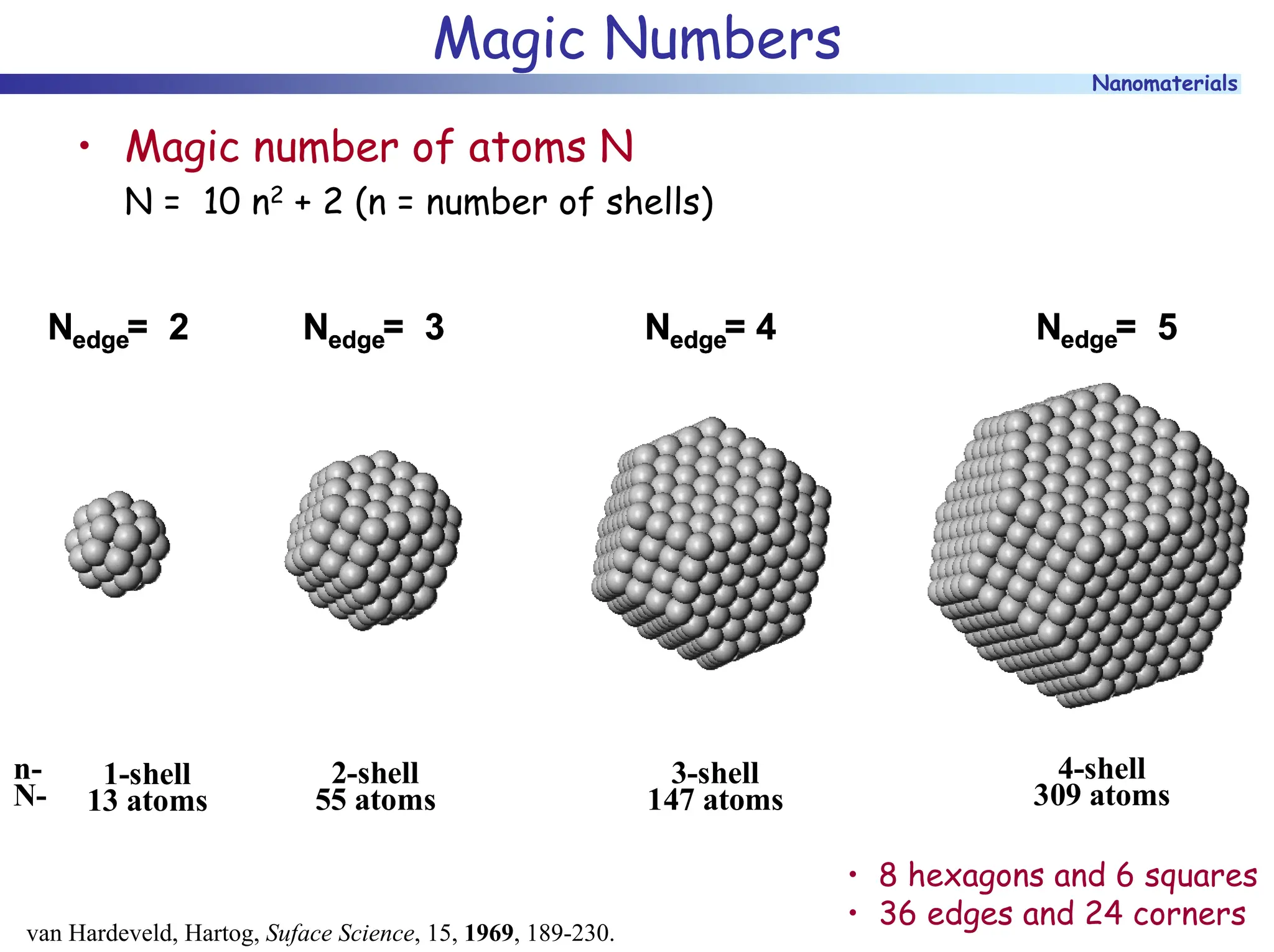
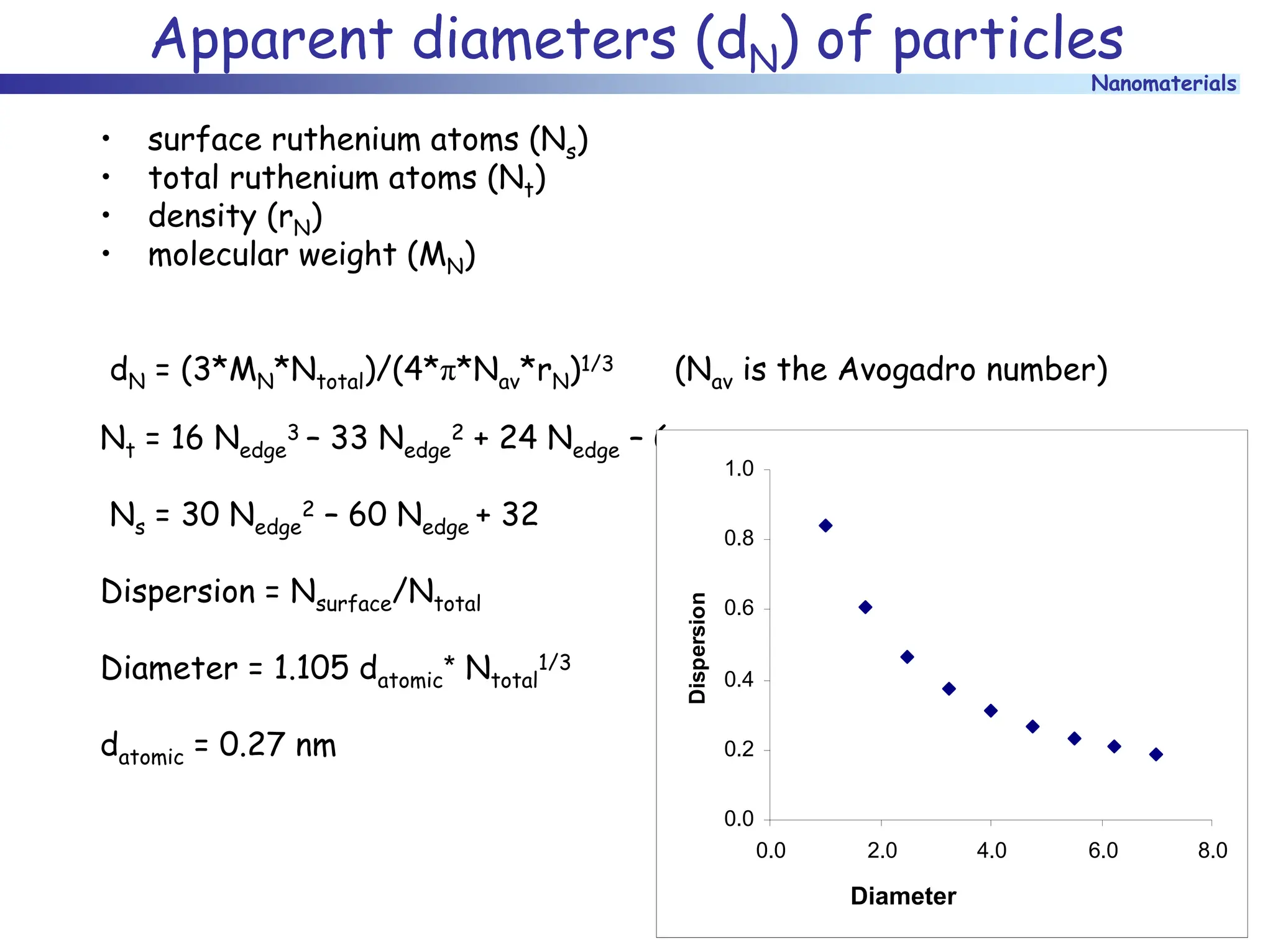
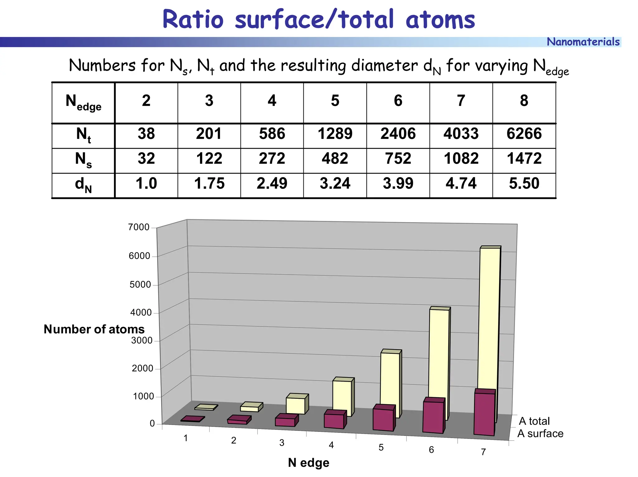
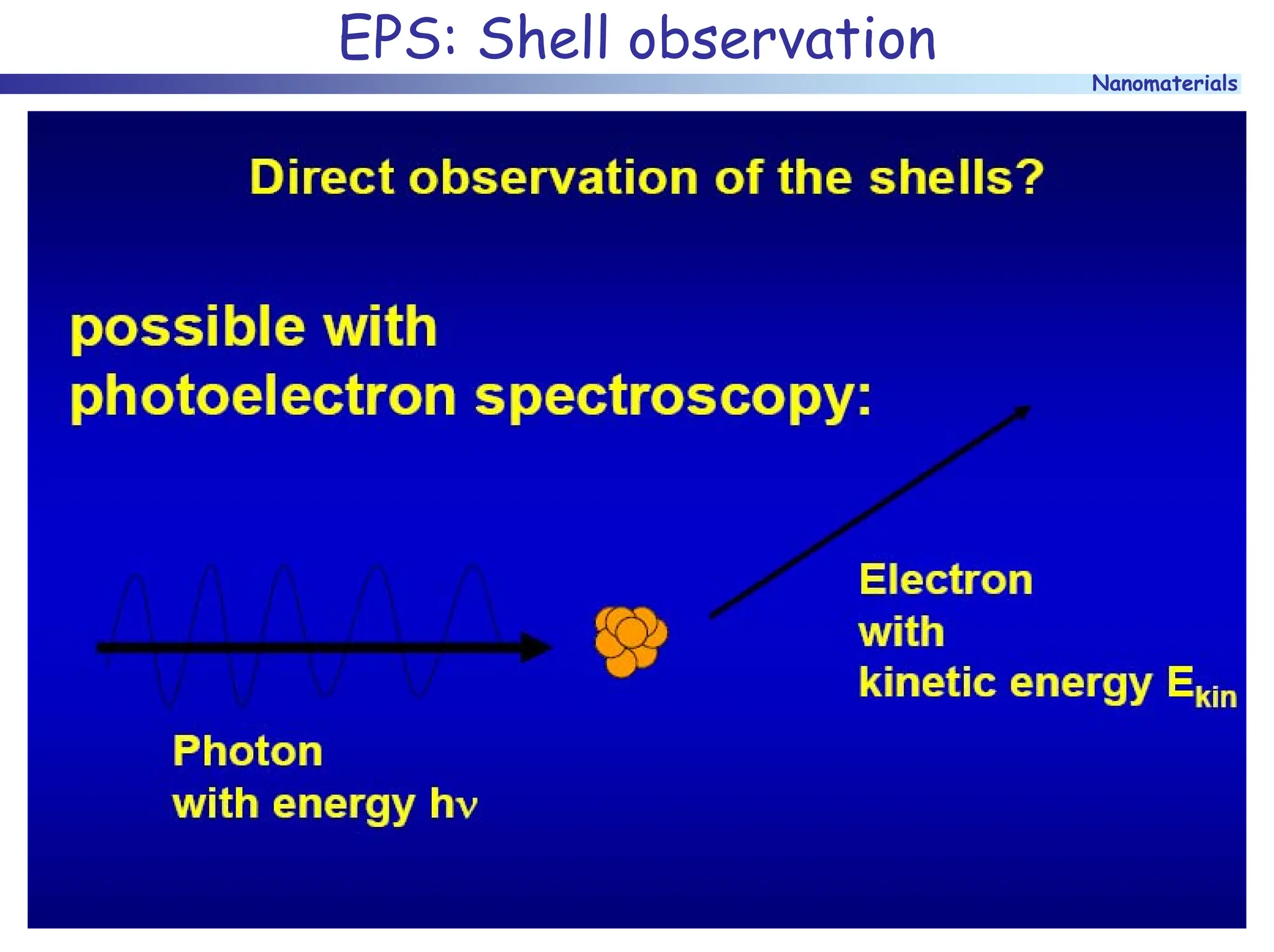
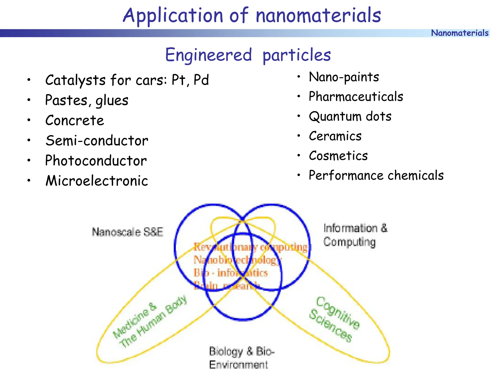
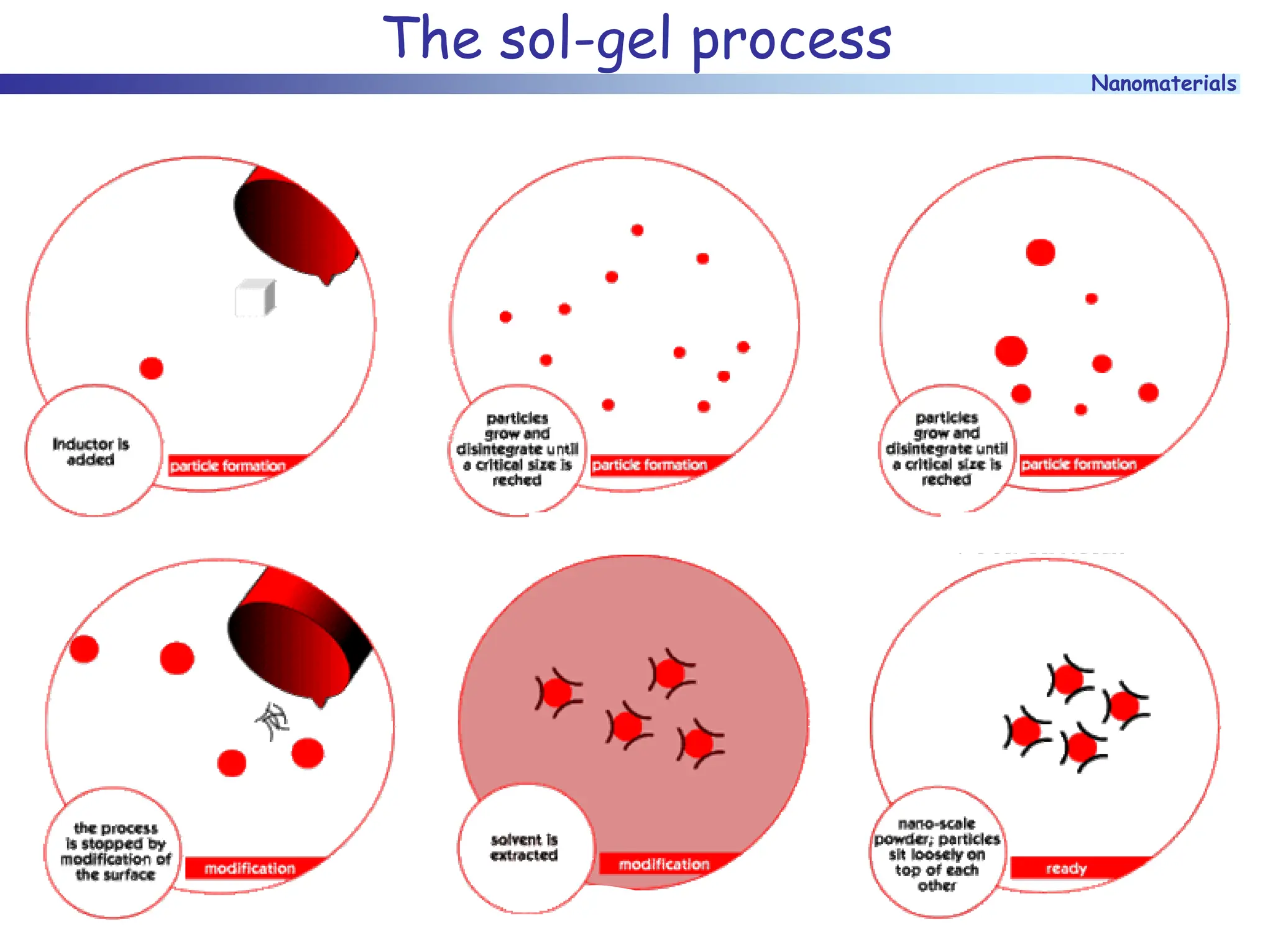
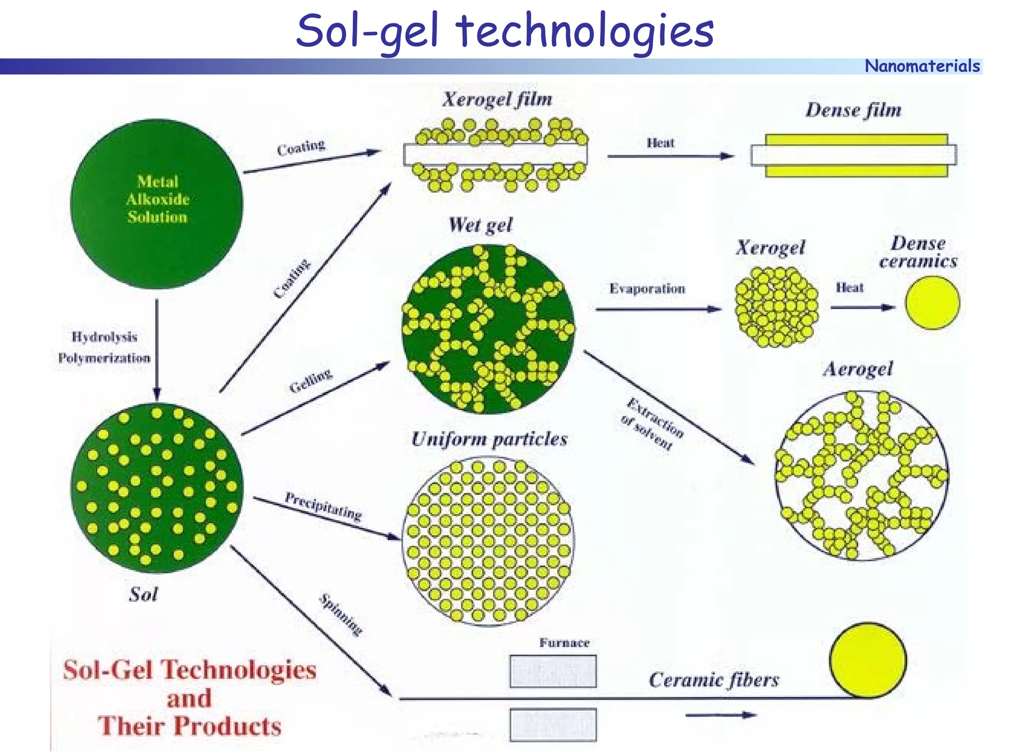
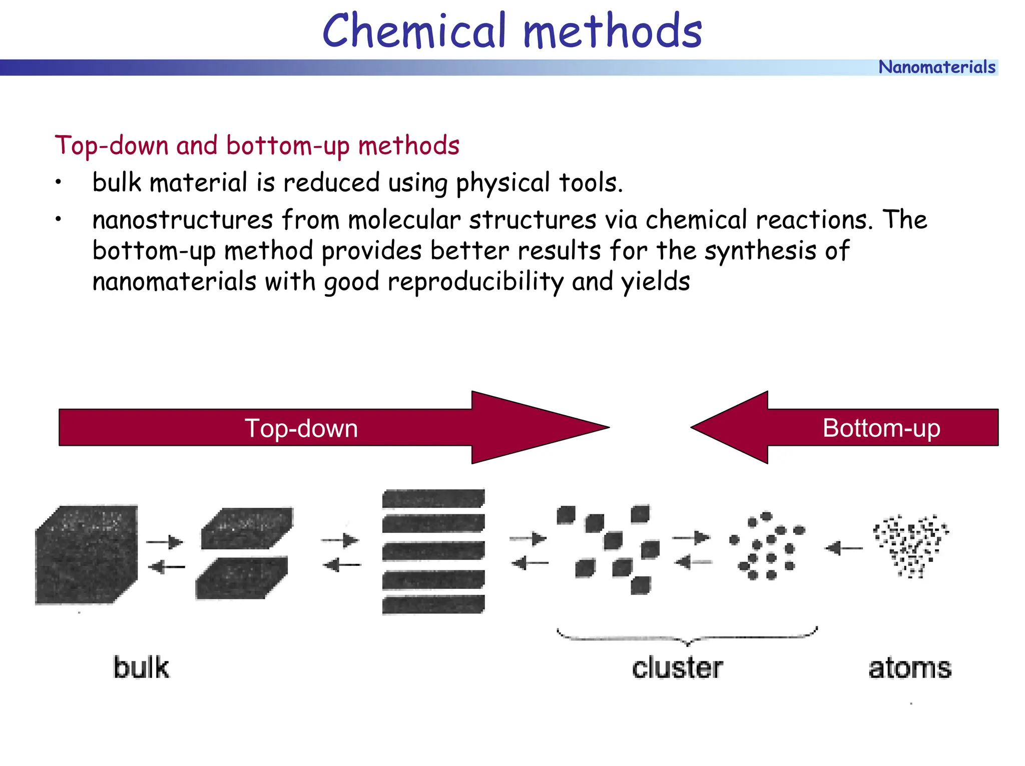
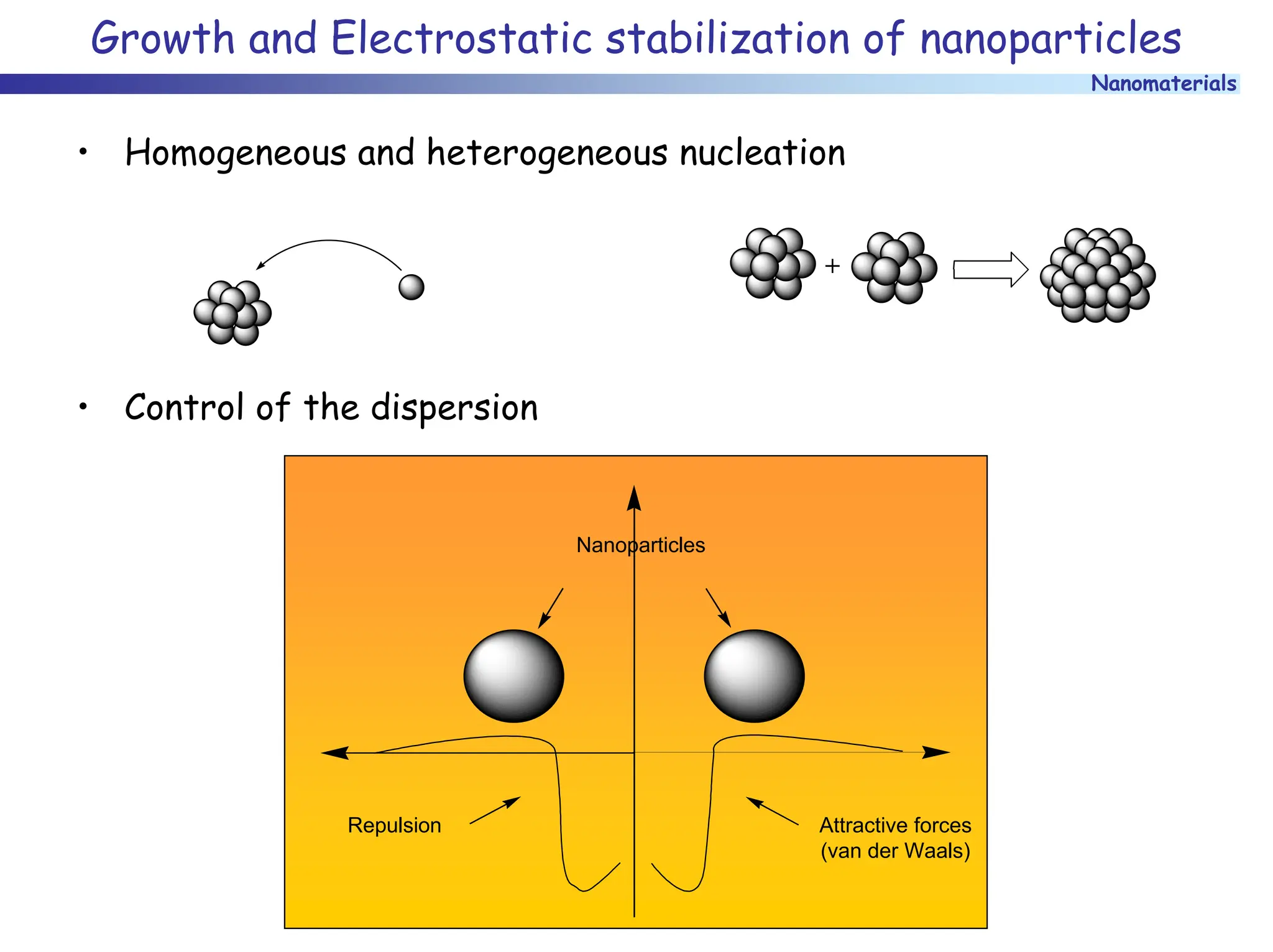
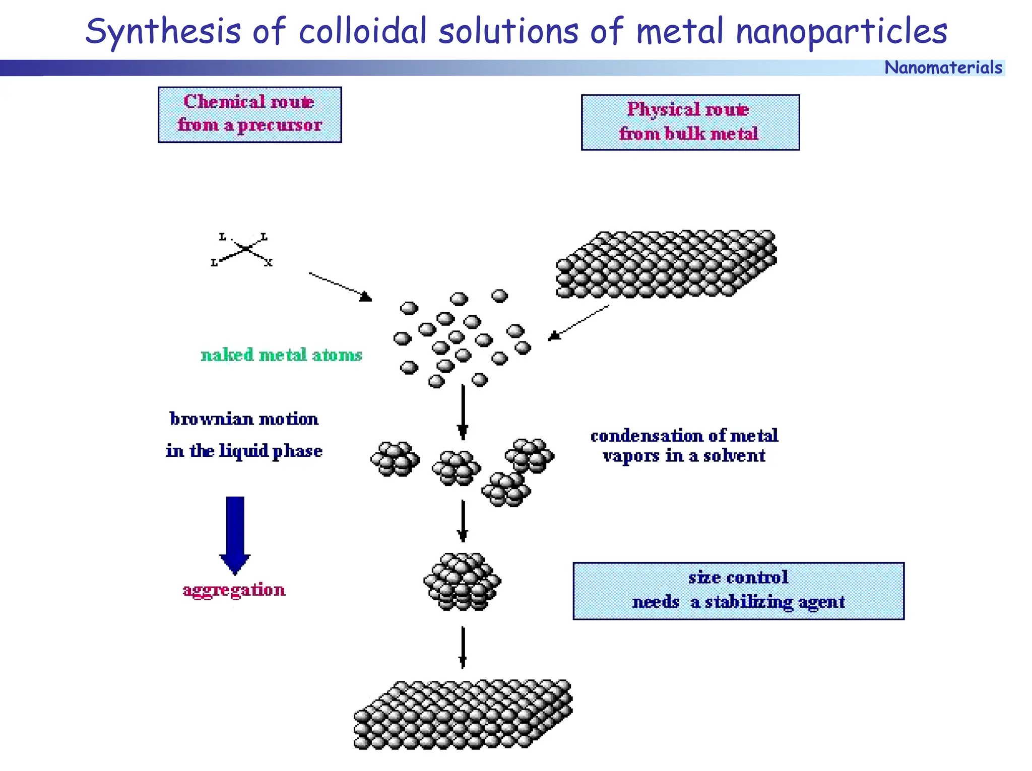
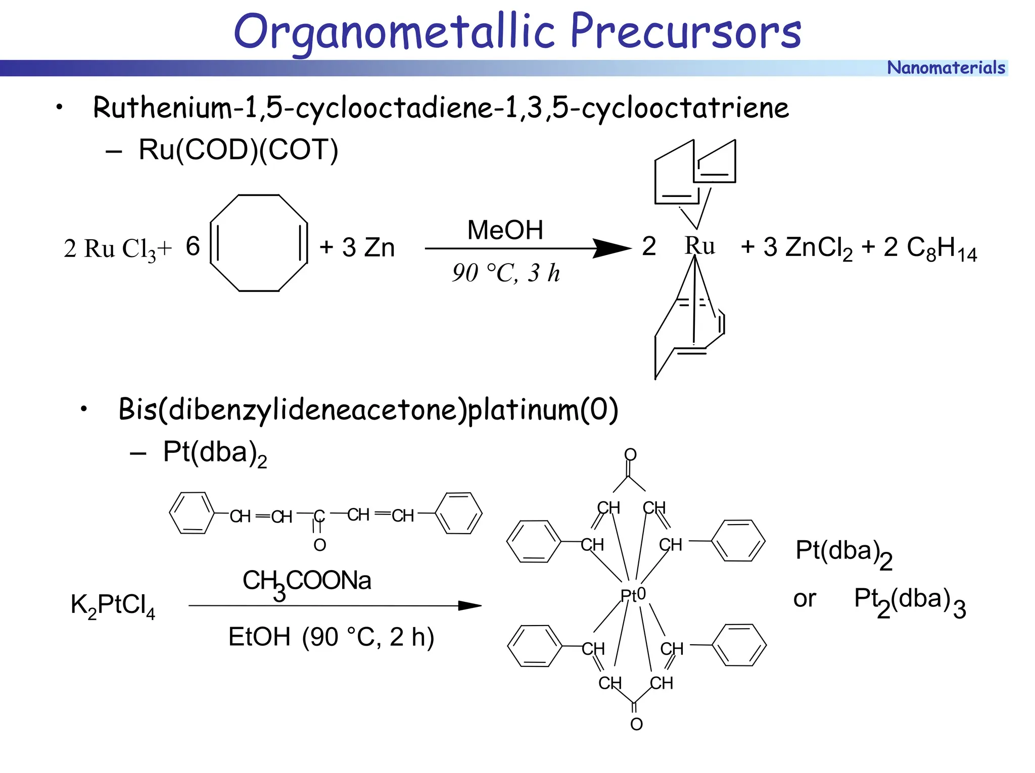
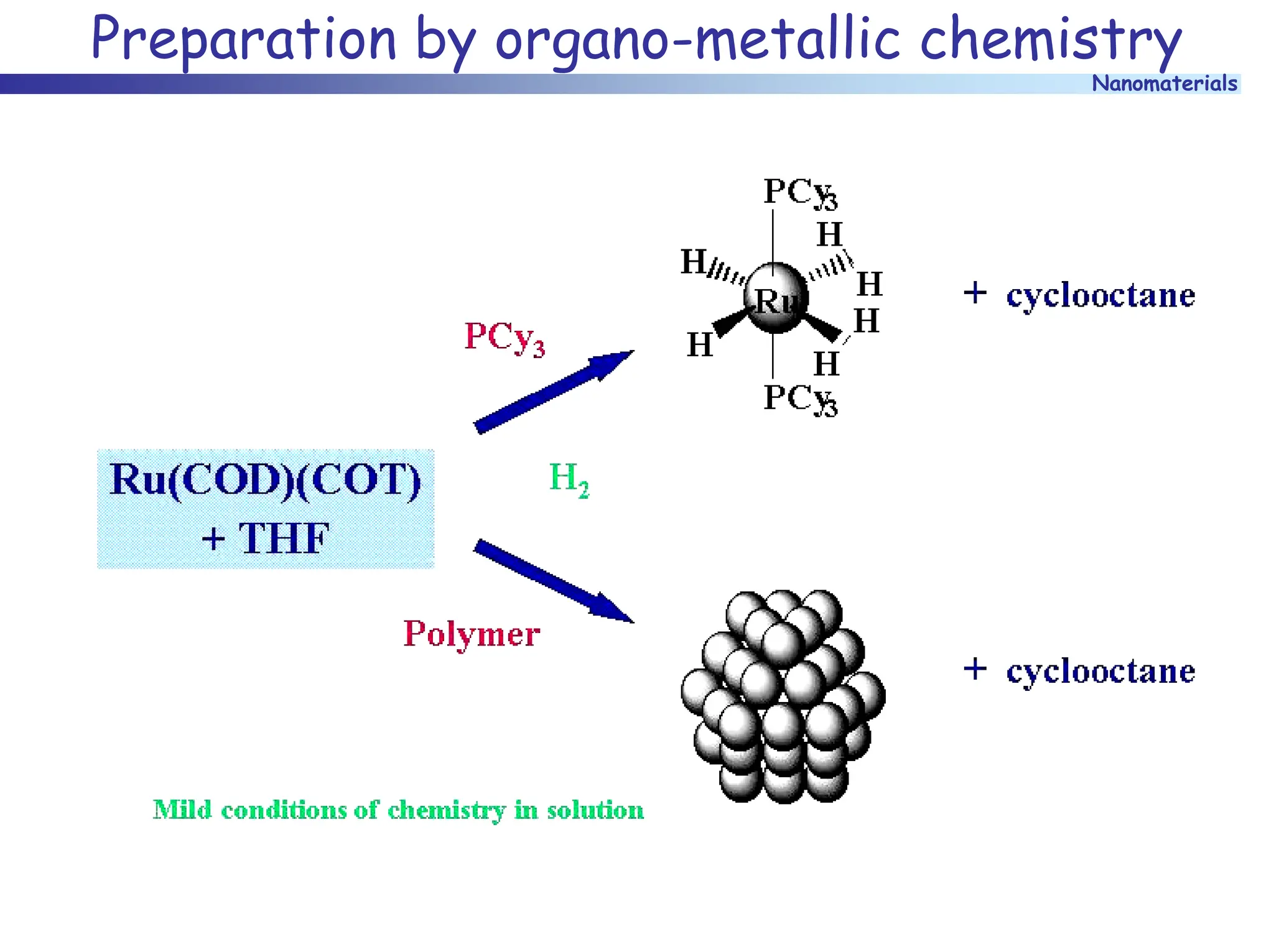
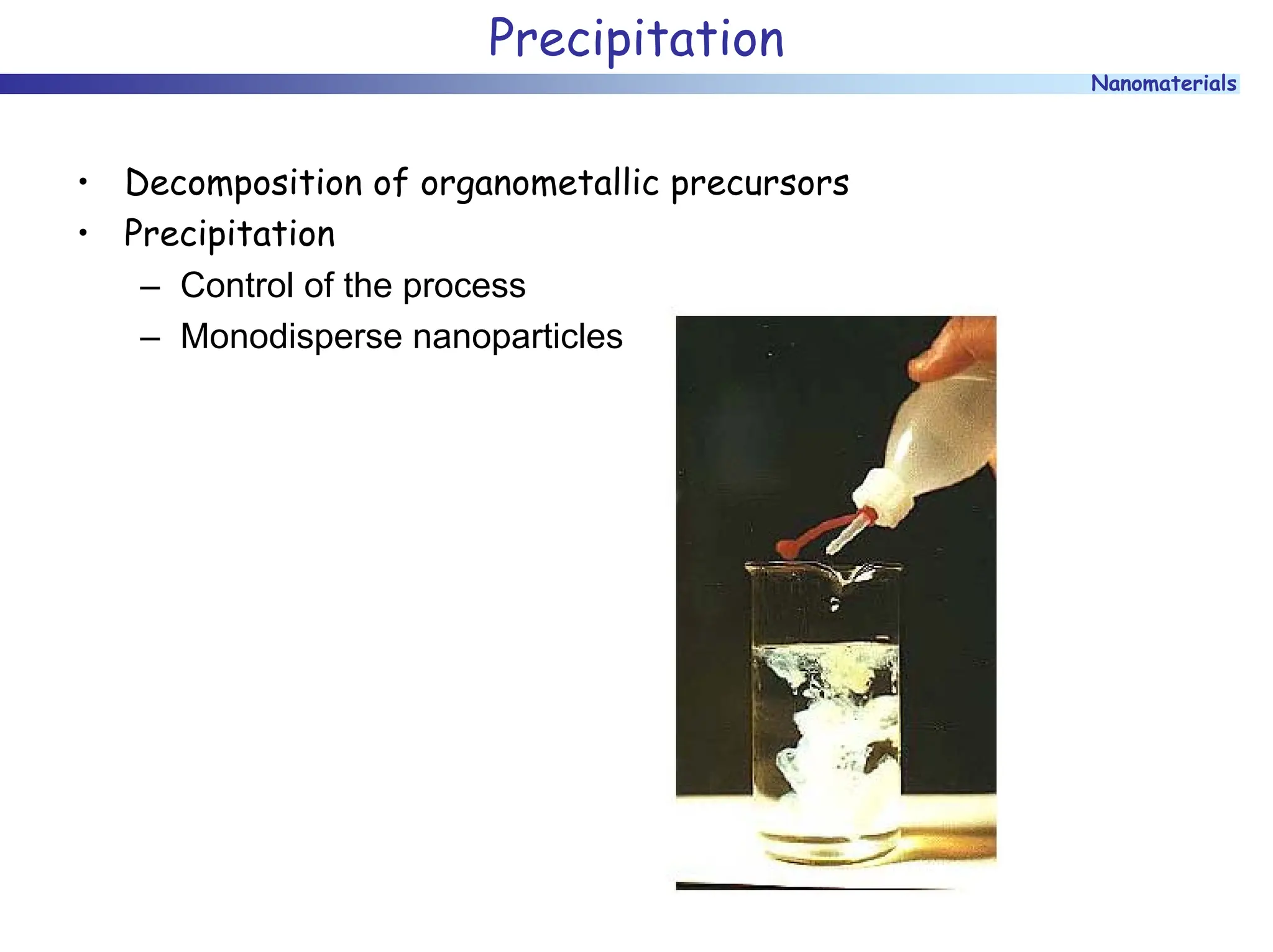
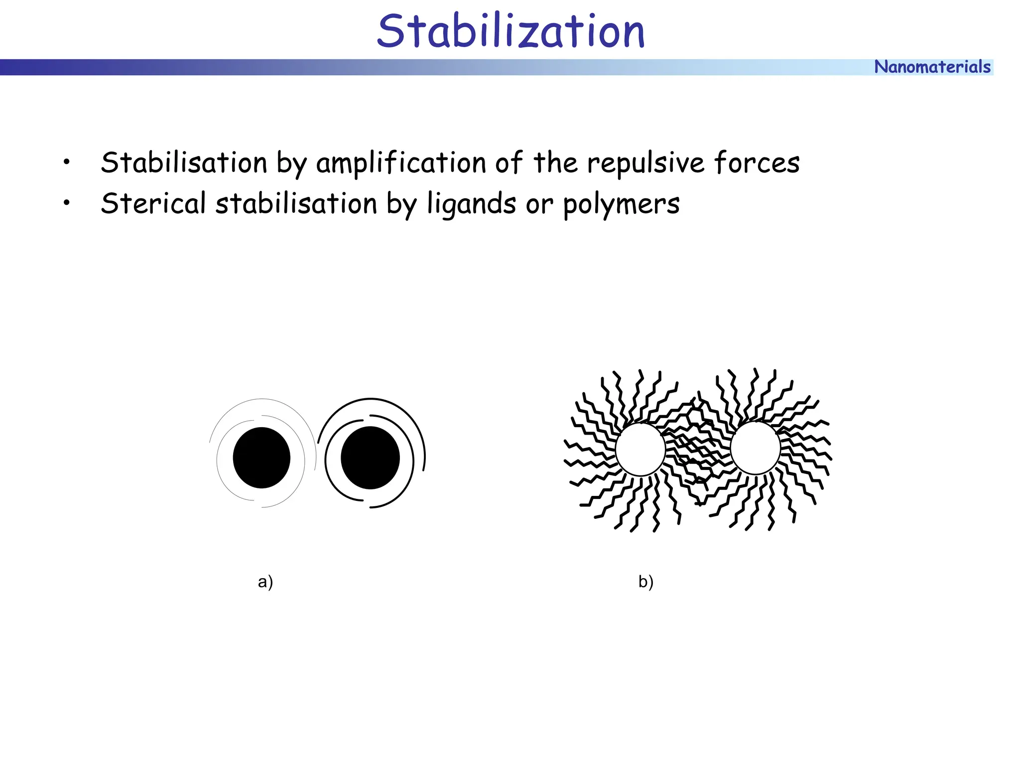
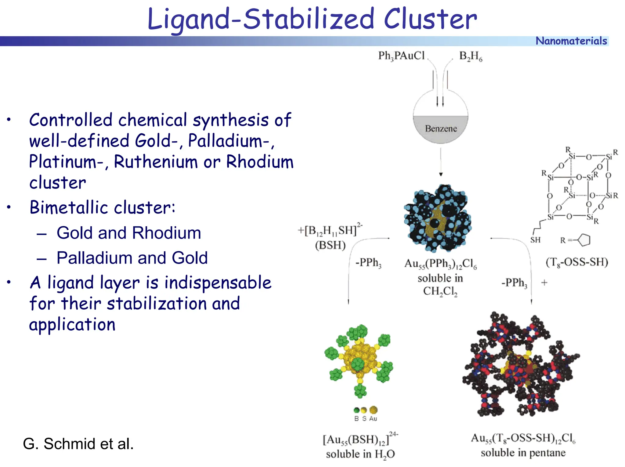
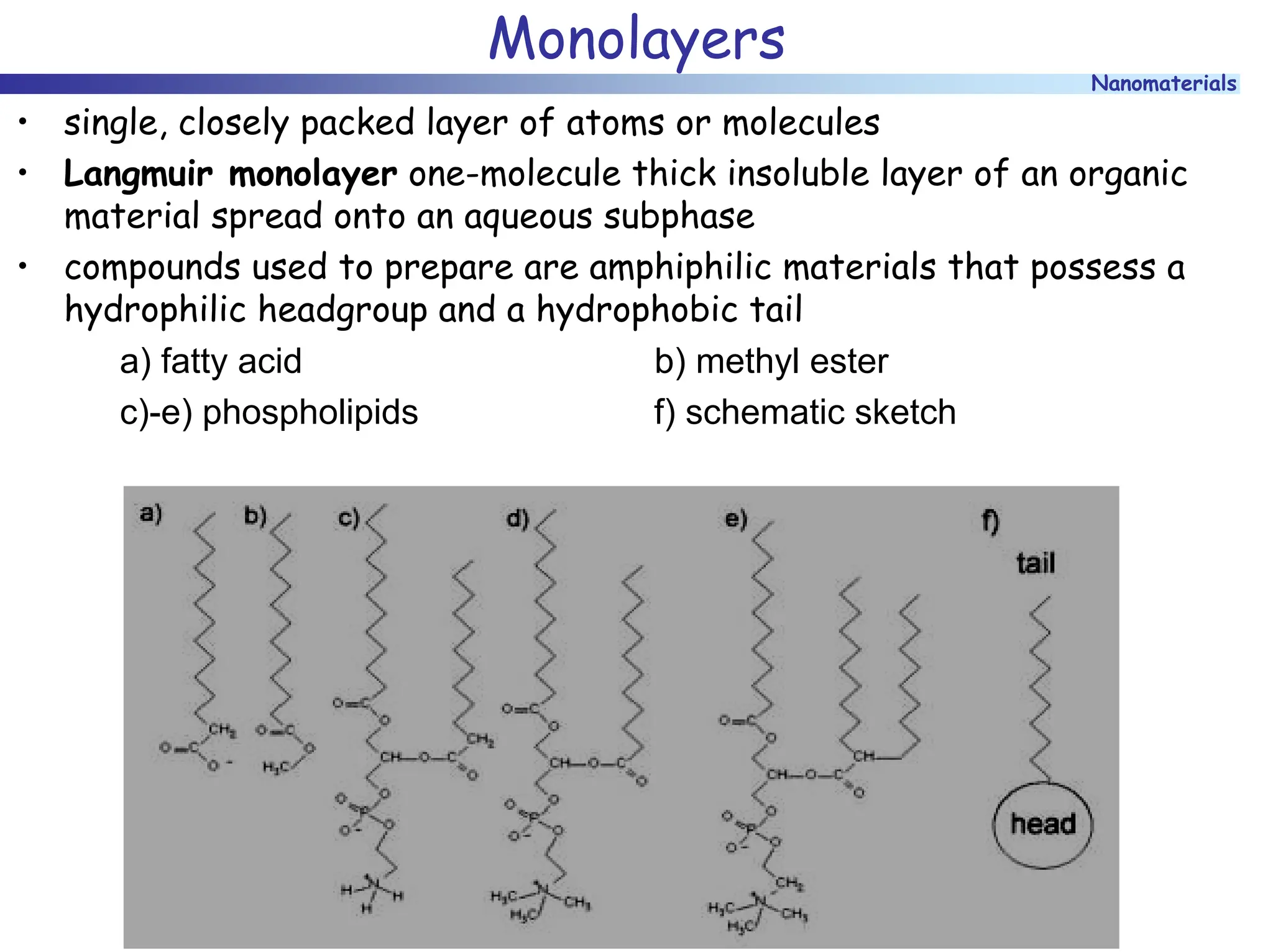
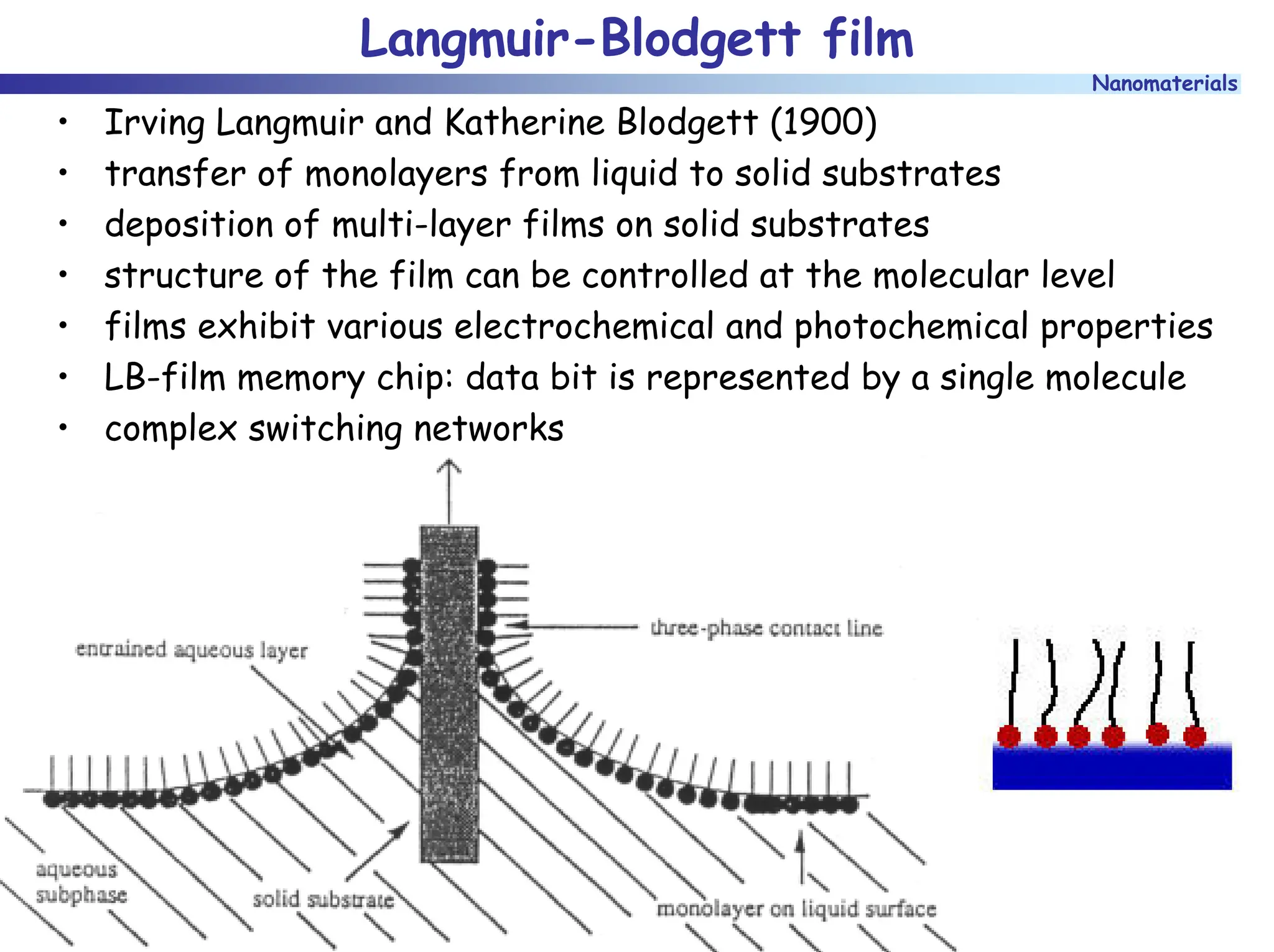
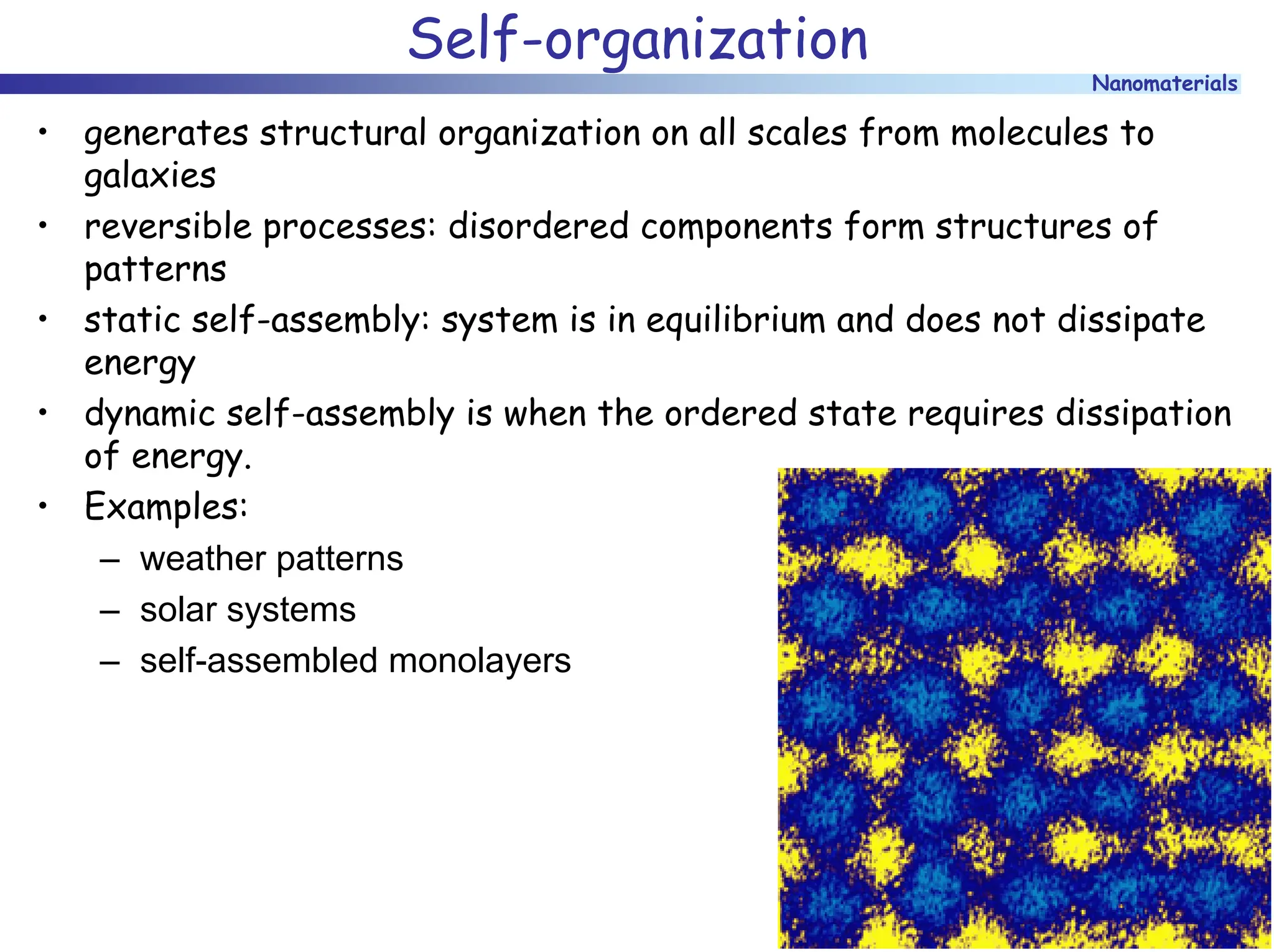
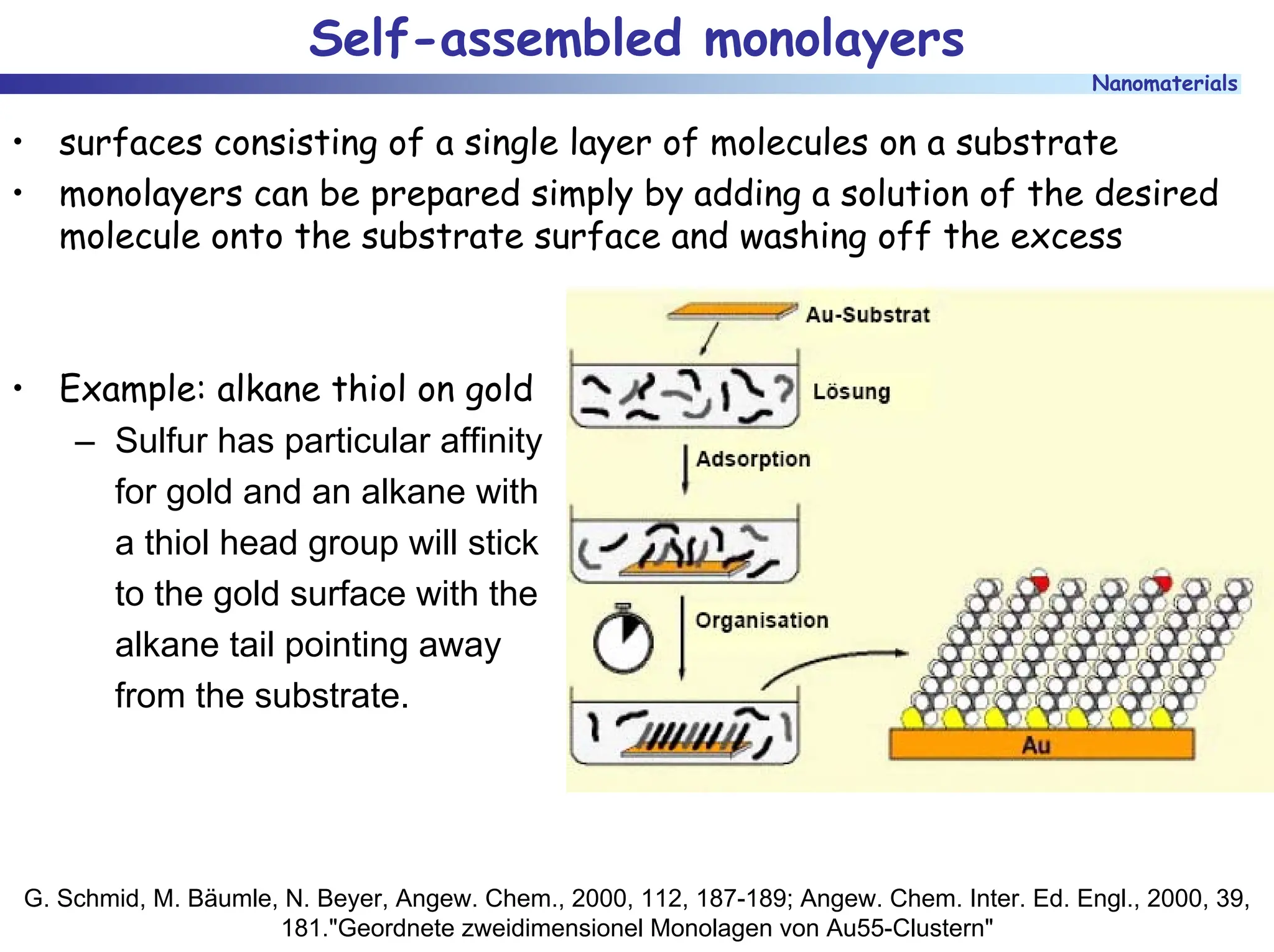
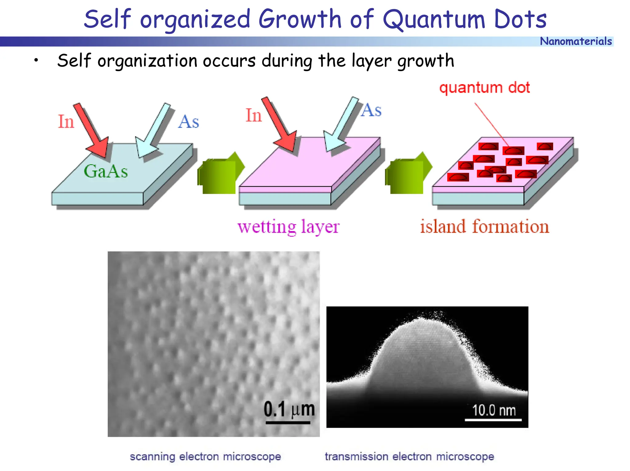
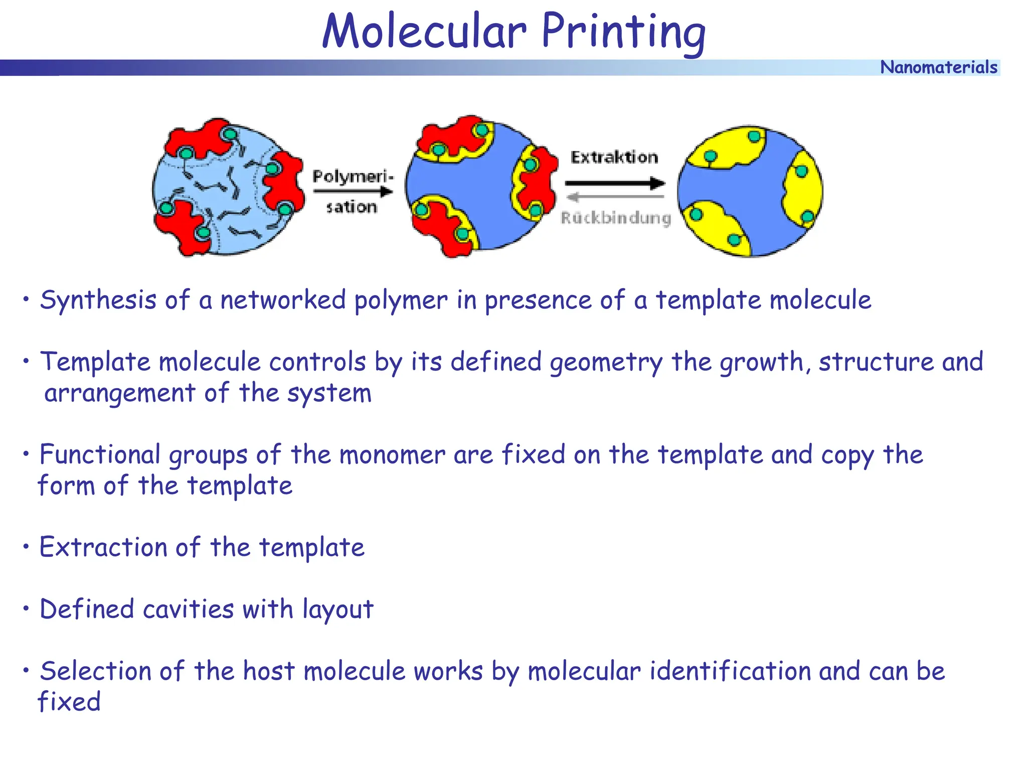
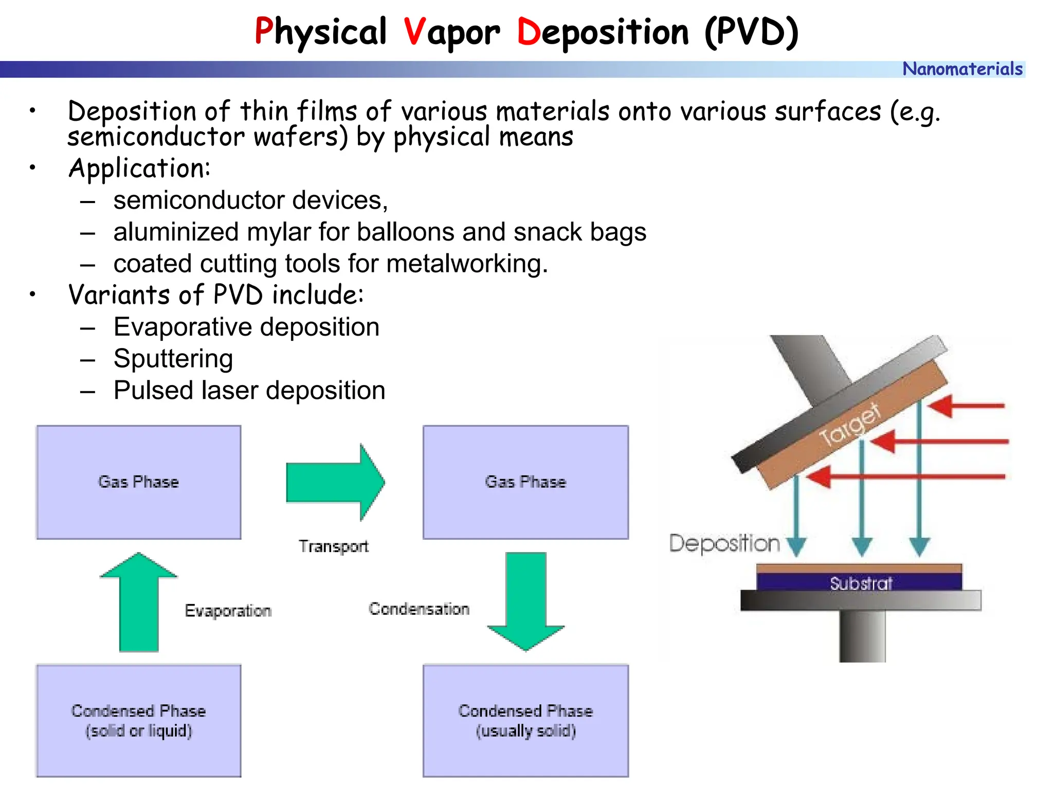
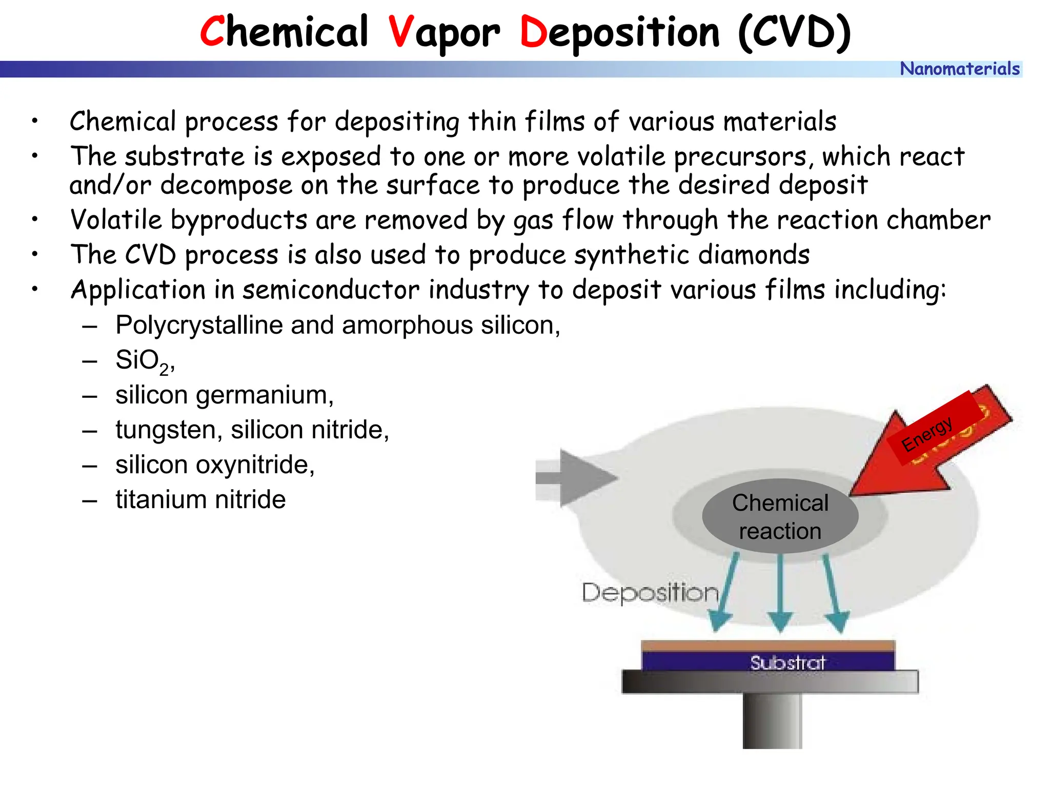
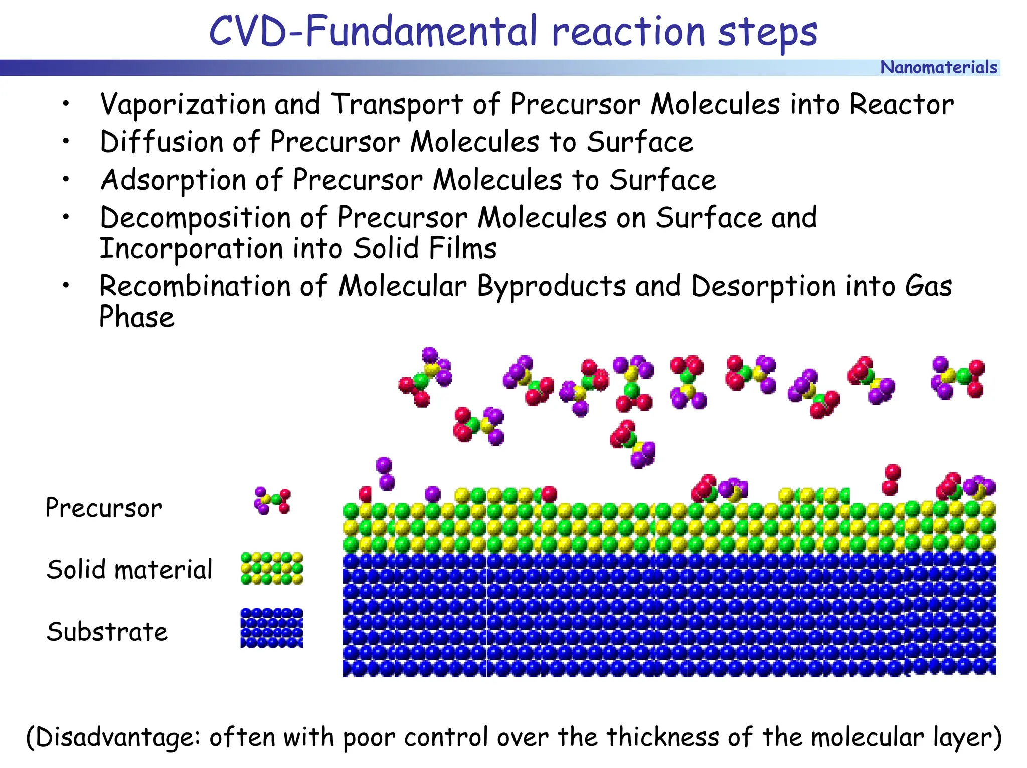
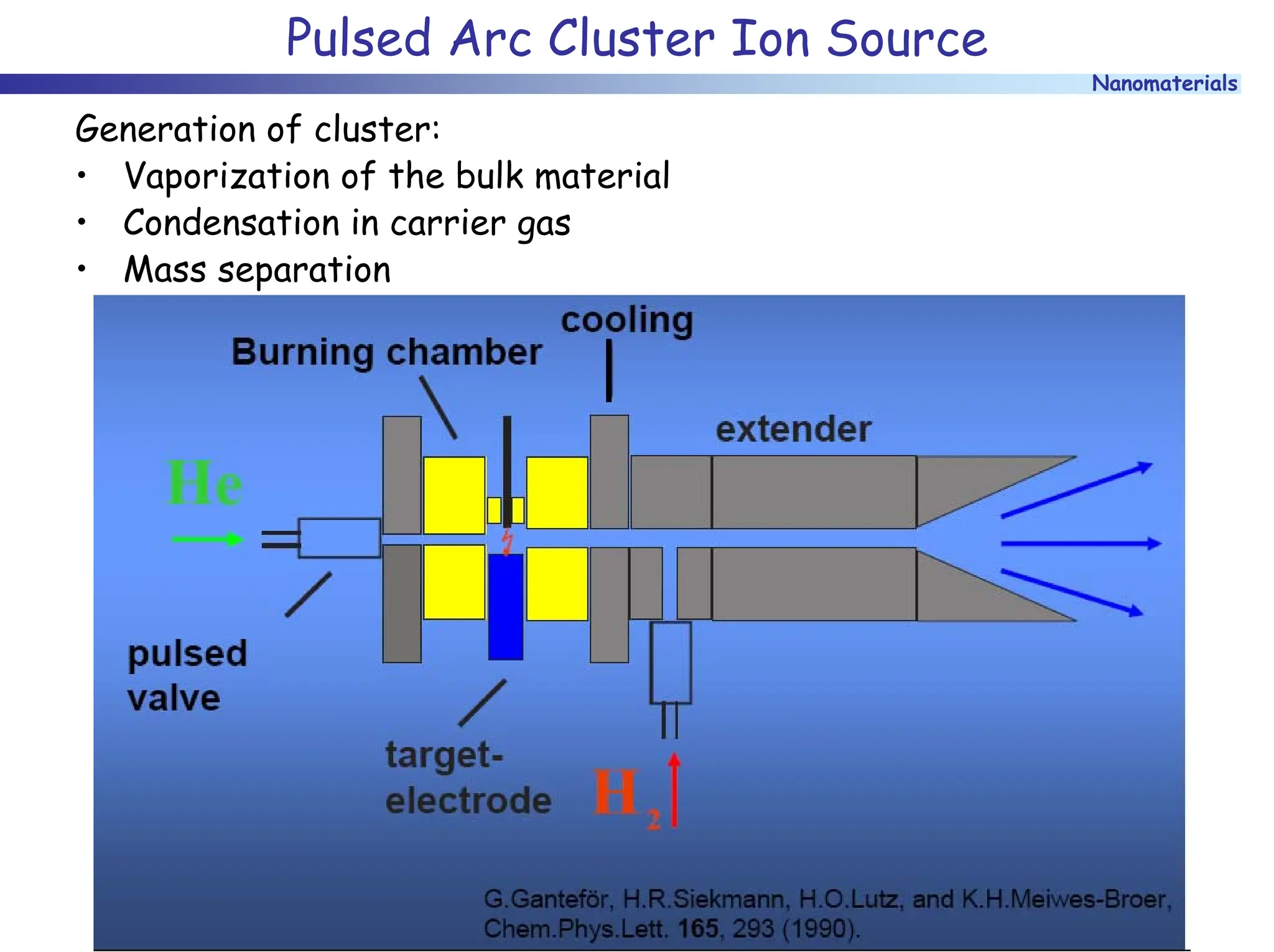
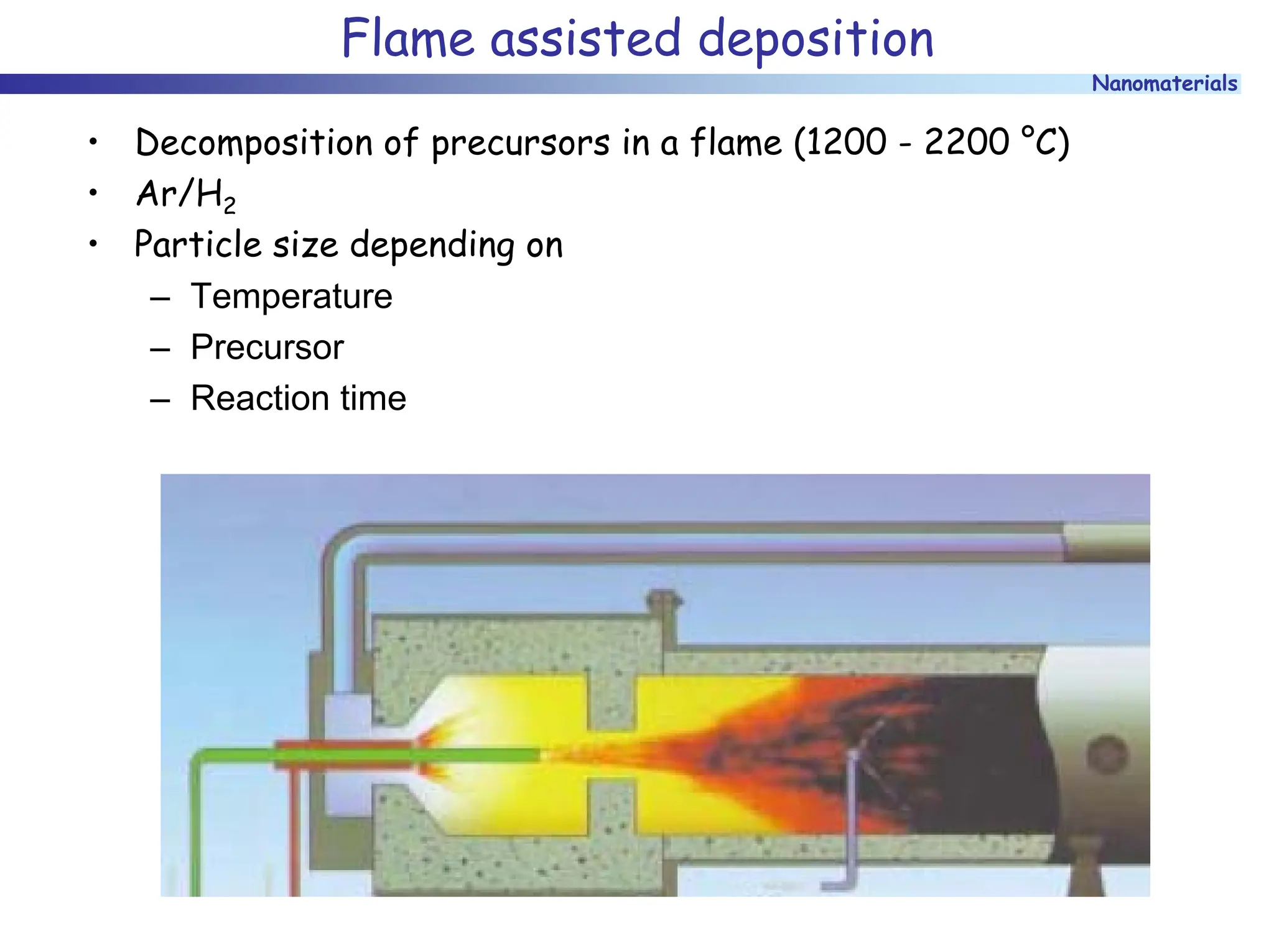
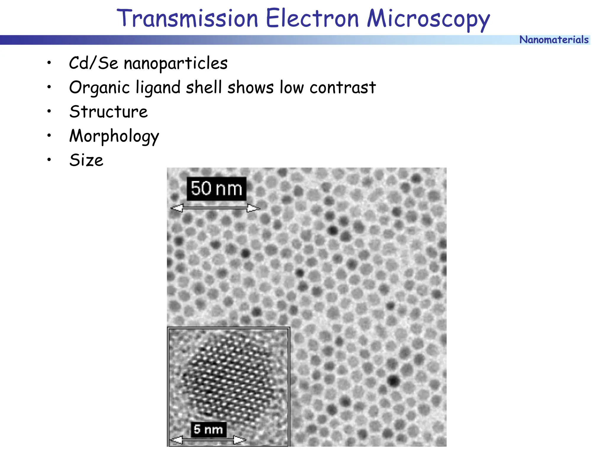
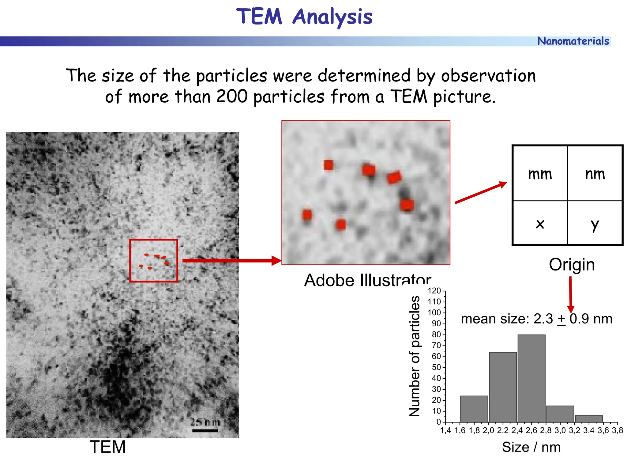
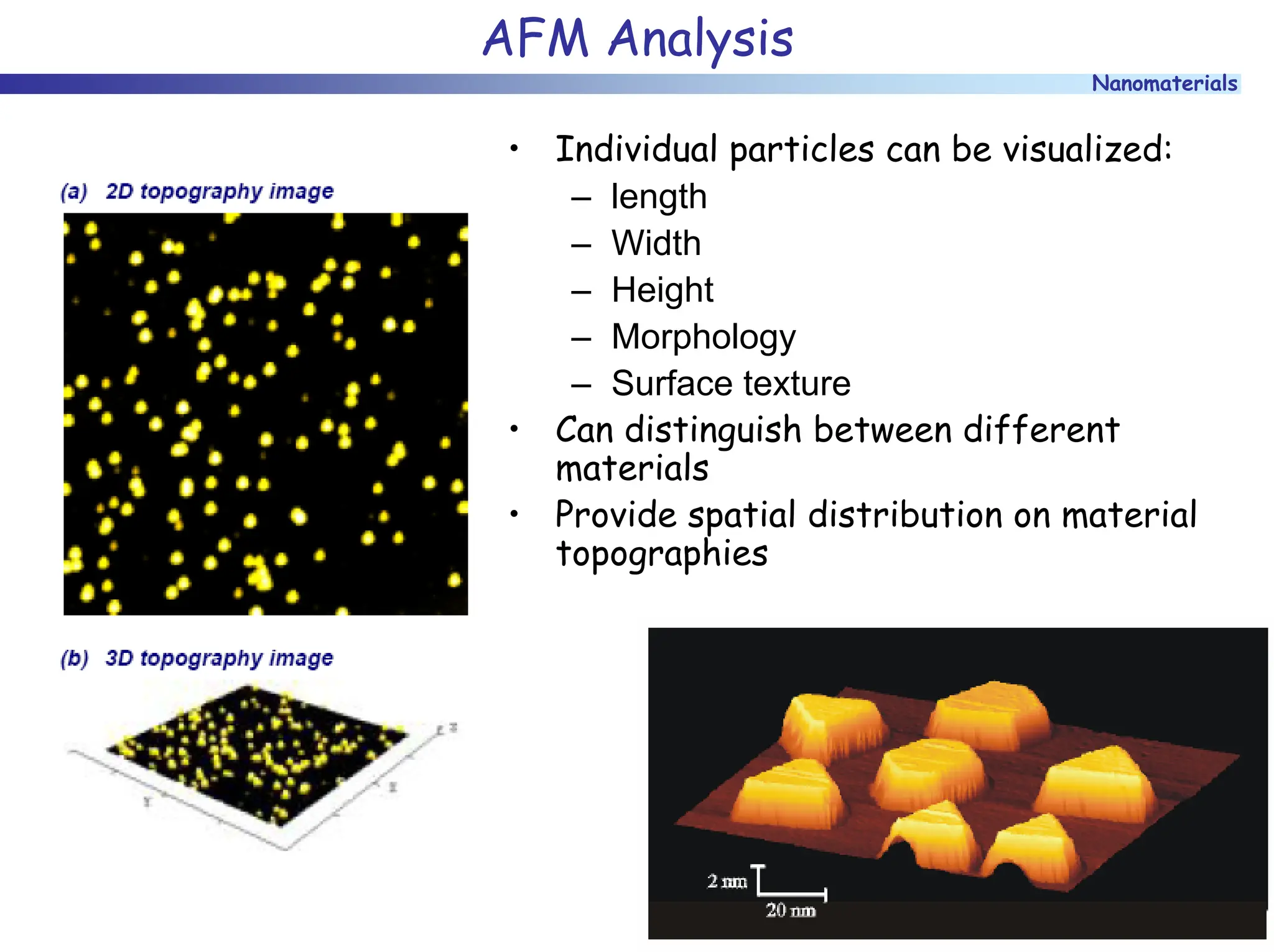
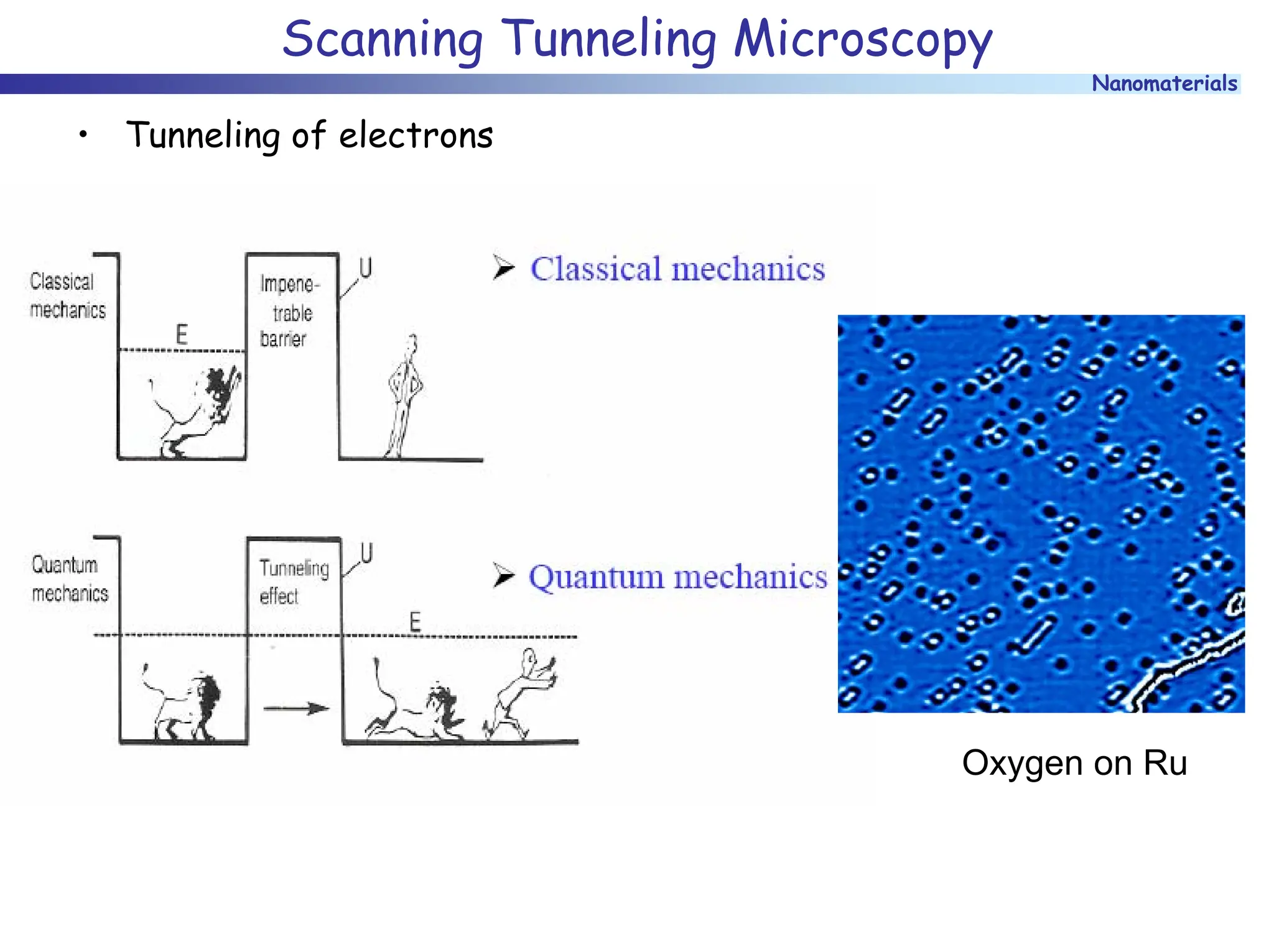
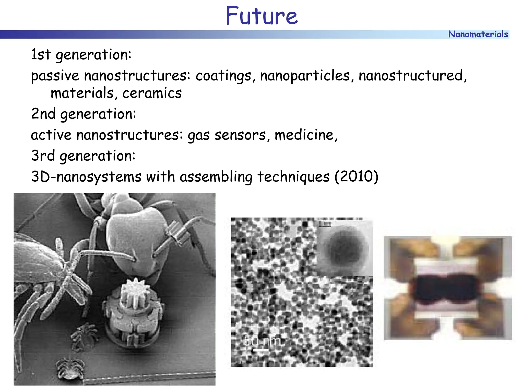
Nanomaterials
Nanomaterials
• Colloids
• Clusters
• Nanoparticles
• Dimensions
• Properties
• Synthesis
• Applications
Nanomaterials
Physical-chemical properties
Nanomaterials
Cluster classification
• Metal: Pt, Fe…
• Covalent: C, Si…
• Ionic: CaI2
• Hydrogen bonding: HF
• Molecule: As4
• Van-der-Waals: He, H2
Nanomaterials
Metallic bond
• Electron delocalization
Nanomaterials
Band model
• Energy levels
Conductor
Isolator Semi-conductor
conduction band
conduction band
conduction band
Band gap
valence band valence band valence band
Nanomaterials
Semi-conductors
Semi-conductor
Valence band
Valence band
Valence band
Conduction band
Conduction band
Conduction band
donator
acceptor
N-dotation
P-dotation
Nanomaterials
Band theory of metals
N = 2
N = 3
N = 4
Cluster Colloid
N = 1 mol
Bulk metal
Atom
• Changing electron levels
changed optical, electronic and catalytic properties
• Properties different from the bulk metal and molecular structures
Nanomaterials
Band gap
Changing metallic properties
Nanomaterials
Band Affiliation
Photoelectronspectra of Hg-:
6s 6p affiliation
Nanomaterials
Quantum size effect
• Change of the electronic properties
• De Broglie wavelength: the freely mobile electrons are very
limited in the reduced dimension
“Size Induced Metal-Insulator Transition”
Nanomaterials
Semiconductor
• Band gap controllable
Nanomaterials
Ionization Potentials and Electron Affinities
IP: Xn → Xn
+ + e- EA: Xn + e- → Xn
-
The bigger radius the less
energy is necessary to remove
an electron
EA is decreasing with the radius
(less surface for a small cluster)
∼ Electron delocalization
Nanomaterials
Ionization Potentials for Na and K
Nanomaterials
Hydrogen Storage
Low IP:
• H2 dissociates
• Hydrid formation
High IP:
• Molecular chemisorption
• Hydrogen storage!!!
Transition from molecular to dissociative chemisorption
Nanomaterials
What are nanoparticles?
• NANO (Greek) = dwarf
• 1 nanometer = 1 nm = 10 -9 m = 0.000000001 m
– Some 1000 atoms or molecules
– Cluster ≤ 1000
• Research: transition of properties from solid state to atoms
– Different chemical and physical properties:
• Electric conductivity
• Chemical reactivity
• Optical properties
• Quantum mechanic rules and not longer classical physics due to their
small size
• Application in catalysis and nanoelectronics
Nanomaterials
What are colloids?
• "Colloid" (Greek: Kolla = glue) 1861 Thomas Graham
• Colloidal Systems:
homogeneous medium and a dispersed material
• “Mesoscopic " dimension: between solid state properties and
molecular effects
• Large specific surface
• New properties by functionalization and configuration
Nanomaterials
Nanochemistry
• For example: Nano-droplet
Drop of liquid water with
50 H2O molecules
Diameter = 1 nm
molecules
Nanomaterials
Snowflake: 1 mm
Nanomaterials
Nanomaterials
From atoms to solids
Nanometer-Scale
A short reminder: 1 nanometer = 1 nm = 10 -9 m = 0.000000001 m
Cluster, Colloids, Nanoparticles
Polymers
Molecules
DNS, virus
Atoms Solids
Proteins
00 102 104 106 108 1010 1012 mass
1 nm 10 nm 100 nm 1µm diameter
1000 m2 100 m2 10 m2 surface
Molecular
chemistry and physics
Cluster and Colloid chemistry Solid state
chemistry and physics
big
molecules
small
solids
Nanomaterials
Rare gas clusters
• Magic numbers of rare gas clusters in MS:
– 13
– 55
– 147
– 309
– 561
• Geometric shell: Mackey Icosahedron
– 5-fold symmetry axis (fcc)
Nanomaterials
Special Nanotypes: Fullerenes
• a large current between two nearby graphite electrodes in an
inert atmosphere
• the resulting carbon plasma arc between the electrodes cools
into sooty residue from which many fullerenes can be isolated
Nanomaterials
Special Nanotypes: Nanotubes
• simple carbon C !
• Diamond: four next neighbors → very stable
• plane and form a honeycomb lattice
• planes are stacked up, to form a solid body
Nanomaterials
Simple metal cluster
• Magic number for neutral atoms (soft metals):
– 8
– 20
– 40
– 58
Nanomaterials
Electronic Effects
Nanomaterials
Geometric effects
Cuboctahedron
• 6 squares and 8 triangles
• 12 corners and 24 edges
• Geometric shells
– Cubic (ccp) or hexagonal (hcp) closed packed
A B C A
A B C A
Coordination number = 12
Nanomaterials
Magic Numbers
• Magic number of atoms N
N = 10 n2 + 2 (n = number of shells)
Nedge= 2
Nedge= 2 Nedge= 3
Nedge= 3 Nedge= 4
Nedge= 4 Nedge= 5
Nedge= 5
Nedge= 2
Nedge= 2
Nedge= 2
Nedge= 2 Nedge= 3
Nedge= 3
Nedge= 3
Nedge= 3 Nedge= 4
Nedge= 4
Nedge= 4
Nedge= 4 Nedge= 5
Nedge= 5
Nedge= 5
Nedge= 5
2-shell
55 atoms
3-shell
147 atoms
4-shell
309 atoms
1-shell
13 atoms
n-
N-
• 8 hexagons and 6 squares
• 36 edges and 24 corners
van Hardeveld, Hartog, Suface Science, 15, 1969, 189-230.
Nanomaterials
Apparent diameters (dN) of particles
• surface ruthenium atoms (Ns)
• total ruthenium atoms (Nt)
• density (rN)
• molecular weight (MN)
dN = (3*MN*Ntotal)/(4*π*Nav*rN)1/3 (Nav is the Avogadro number)
Nt = 16 Nedge
3 – 33 Nedge
2 + 24 Nedge – 6
Ns = 30 Nedge
2 – 60 Nedge + 32
Dispersion = Nsurface/Ntotal
Diameter = 1.105 datomic* Ntotal
1/3
datomic = 0.27 nm
0.0
0.2
0.4
0.6
0.8
1.0
0.0 2.0 4.0 6.0 8.0
Diamère apparent
Dispersion
Diameter
Nanomaterials
Ratio surface/total atoms
Numbers for Ns, Nt and the resulting diameter dN for varying Nedge
Nedge 2 3 4 5 6 7 8
Nt 38 201 586 1289 2406 4033 6266
Ns 32 122 272 482 752 1082 1472
dN 1.0 1.75 2.49 3.24 3.99 4.74 5.50
1 2 3 4 5 6 7
A surface
A total
0
1000
2000
3000
4000
5000
6000
7000
Number of atoms
N edge
Nanomaterials
EPS: Shell observation
Nanomaterials
Application of nanomaterials
Engineered particles
• Nano-paints
• Pharmaceuticals
• Quantum dots
• Ceramics
• Cosmetics
• Performance chemicals
• Catalysts for cars: Pt, Pd
• Pastes, glues
• Concrete
• Semi-conductor
• Photoconductor
• Microelectronic
Nanomaterials
Preparation of Nanomaterials
• Lithography
• Sol-Gel-process
• Flame assisted deposition
• Gas phase deposition (CVD, PVD)
• Chemical preparation in solution e.g. reduction of different
metal complexes by BH or H2 in solution
• Self-assembled monolayers (SAM)
• Precipitation
Defined and narrow size distribution
Best results: Synthesis in solution and self assembly
Nanomaterials
Lithography
Principle
• based on the repulsion of oil and water
• image is placed on the surface with an oil-based medium
• acid 'burns' the oil into the surface
• water remains on the non-oily surface and avoids the oily
parts
• a roller applies an oil-based ink that adheres only to the oily
portion of the surface
Nanomaterials
Lithography
Modern technique
• A fused silica surface, covered with
a release layer, is pressed into a
thin layer of a silicon-containing
monomer
• Illumination by a UV lamp
polymerizes the surface into a hard
material
• Upon separation of the fused silica
template, the circuit pattern is left
on the surface
• A residual layer of polymer between
features is eliminated by an etch
process
• Template fabrication process limits
the resolution of the features
(20 nm)
Nanomaterials
Sol-gel process
• Formation of a colloidal suspension (sol) and gelation to form a
network in a continuous liquid phase (gel)
• precursors for these colloids consist of a metal or metalloid
element surrounded by various reactive ligands
Metal alkoxides: alkoxysilanes, such as tetramethoxysilane
(TMOS) and tetraethoxysilane (TEOS).
• three reactions: hydrolysis, alcohol and water condensation
Lev, O. et al. Analytical Chemistry. 1995, 67(1), 22A-30A.
K.D. Keefer, in: Silicon Based Polymer Science: A Comprehensive Resource; eds. J.M. Zeigler and F.W.G. Fearon, ACS
Advances in Chemistry Ser. No. 224, (American Chemical Society: Washington, DC, 1990) pp. 227-240.
Nanomaterials
Sol-gel polymerization: three stages
1. Polymerization of monomers to form particles
2. Growth of particles
3. Linking of particles into chains, then networks
• many factors affect the resulting silica network:
– pH
– temperature
– time of reaction
– reagent concentrations
– catalyst nature and concentration
– H2O/Si molar ratio
– aging temperature and time
Nanomaterials
The sol-gel process
Nanomaterials
Sol-gel technologies
Nanomaterials
Chemical methods
Top-down and bottom-up methods
• bulk material is reduced using physical tools.
• nanostructures from molecular structures via chemical reactions. The
bottom-up method provides better results for the synthesis of
nanomaterials with good reproducibility and yields
Top-down Bottom-up
Growth and Electrostatic stabilization of nanoparticles
Nanomaterials
• Homogeneous and heterogeneous nucleation
• Control of the dispersion
+
Repulsion Attractive forces
(van der Waals)
Nanoparticles
Nanomaterials
Synthesis of colloids
• Radiation induced synthesis of colloids
• Electrochemical synthesis of colloids
• Ultrasound-assisted electrochemical synthesis
• Salt reduction
• Organo-metallic synthesis
(thermal decomposition, ligand reduction or ligand displacement)
Nanomaterials
Synthesis of colloidal solutions of metal nanoparticles
Nanomaterials
Organometallic Precursors
• Ruthenium-1,5-cyclooctadiene-1,3,5-cyclooctatriene
– Ru(COD)(COT)
2 Ru Cl3+ Ru
90 °C, 3 h
6 + 3 ZnCl2 + 2 C8H14
+ 3 Zn 2
MeOH
• Bis(dibenzylideneacetone)platinum(0)
– Pt(dba)2
CH
CH CH
CH
Pt0
CH CH
CH
O
CH
O
CH CH C
O
CH CH
CH
3COONa
EtOH (90 °C, 2 h)
Pt(dba)2
or Pt2(dba)3
K2PtCl4
Nanomaterials
Preparation by organo-metallic chemistry
Nanomaterials
Precipitation
• Decomposition of organometallic precursors
• Precipitation
– Control of the process
– Monodisperse nanoparticles
Nanomaterials
Stabilization
• Stabilisation by amplification of the repulsive forces
• Sterical stabilisation by ligands or polymers
a) b)
Nanomaterials
Ligand-Stabilized Cluster
• Controlled chemical synthesis of
well-defined Gold-, Palladium-,
Platinum-, Ruthenium or Rhodium
cluster
• Bimetallic cluster:
– Gold and Rhodium
– Palladium and Gold
• A ligand layer is indispensable
for their stabilization and
application
G. Schmid et al.
Nanomaterials
Monolayers
• single, closely packed layer of atoms or molecules
• Langmuir monolayer one-molecule thick insoluble layer of an organic
material spread onto an aqueous subphase
• compounds used to prepare are amphiphilic materials that possess a
hydrophilic headgroup and a hydrophobic tail
a) fatty acid b) methyl ester
c)-e) phospholipids f) schematic sketch
Nanomaterials
Langmuir-Blodgett film
• Irving Langmuir and Katherine Blodgett (1900)
• transfer of monolayers from liquid to solid substrates
• deposition of multi-layer films on solid substrates
• structure of the film can be controlled at the molecular level
• films exhibit various electrochemical and photochemical properties
• LB-film memory chip: data bit is represented by a single molecule
• complex switching networks
Nanomaterials
Self-organization
• generates structural organization on all scales from molecules to
galaxies
• reversible processes: disordered components form structures of
patterns
• static self-assembly: system is in equilibrium and does not dissipate
energy
• dynamic self-assembly is when the ordered state requires dissipation
of energy.
• Examples:
– weather patterns
– solar systems
– self-assembled monolayers
Nanomaterials
Self-assembled monolayers
• surfaces consisting of a single layer of molecules on a substrate
• monolayers can be prepared simply by adding a solution of the desired
molecule onto the substrate surface and washing off the excess
• Example: alkane thiol on gold
– Sulfur has particular affinity
for gold and an alkane with
a thiol head group will stick
to the gold surface with the
alkane tail pointing away
from the substrate.
G. Schmid, M. Bäumle, N. Beyer, Angew. Chem., 2000, 112, 187-189; Angew. Chem. Inter. Ed. Engl., 2000, 39,
181."Geordnete zweidimensionel Monolagen von Au55-Clustern"
Nanomaterials
Self organized Growth of Quantum Dots
• Self organization occurs during the layer growth
Nanomaterials
Molecular Printing
• Synthesis of a networked polymer in presence of a template molecule
• Template molecule controls by its defined geometry the growth, structure and
arrangement of the system
• Functional groups of the monomer are fixed on the template and copy the
form of the template
• Extraction of the template
• Defined cavities with layout
• Selection of the host molecule works by molecular identification and can be
fixed
Nanomaterials
Physical Vapor Deposition (PVD)
• Deposition of thin films of various materials onto various surfaces (e.g.
semiconductor wafers) by physical means
• Application:
– semiconductor devices,
– aluminized mylar for balloons and snack bags
– coated cutting tools for metalworking.
• Variants of PVD include:
– Evaporative deposition
– Sputtering
– Pulsed laser deposition
Nanomaterials
Chemical Vapor Deposition (CVD)
• Chemical process for depositing thin films of various materials
• The substrate is exposed to one or more volatile precursors, which react
and/or decompose on the surface to produce the desired deposit
• Volatile byproducts are removed by gas flow through the reaction chamber
• The CVD process is also used to produce synthetic diamonds
• Application in semiconductor industry to deposit various films including:
– Polycrystalline and amorphous silicon,
– SiO2,
– silicon germanium,
– tungsten, silicon nitride,
– silicon oxynitride,
– titanium nitride
Energy
Chemical
reaction
Nanomaterials
CVD-Fundamental reaction steps
• Vaporization and Transport of Precursor Molecules into Reactor
• Diffusion of Precursor Molecules to Surface
• Adsorption of Precursor Molecules to Surface
• Decomposition of Precursor Molecules on Surface and
Incorporation into Solid Films
• Recombination of Molecular Byproducts and Desorption into Gas
Phase
Precursor
Solid material
Substrate
(Disadvantage: often with poor control over the thickness of the molecular layer)
Nanomaterials
Pulsed Arc Cluster Ion Source
Generation of cluster:
• Vaporization of the bulk material
• Condensation in carrier gas
• Mass separation
Nanomaterials
Flame assisted deposition
• Decomposition of precursors in a flame (1200 - 2200 °C)
• Ar/H2
• Particle size depending on
– Temperature
– Precursor
– Reaction time
Nanomaterials
Transmission Electron Microscopy
• Cd/Se nanoparticles
• Organic ligand shell shows low contrast
• Structure
• Morphology
• Size
Nanomaterials
TEM Analysis
The size of the particles were determined by observation
of more than 200 particles from a TEM picture.
Adobe Illustrator
mm nm
x y
Origin
TEM
1,4 1,6 1,8 2,0 2,2 2,4 2,6 2,8 3,0 3,2 3,4 3,6 3,8
0
10
20
30
40
50
60
70
80
90
100
110
120
mean size: 2.3 + 0.9 nm
Number
of
particles Size / nm
Nanomaterials
AFM Analysis
• Individual particles can be visualized:
– length
– Width
– Height
– Morphology
– Surface texture
• Can distinguish between different
materials
• Provide spatial distribution on material
topographies
Nanomaterials
Scanning Tunneling Microscopy
• Tunneling of electrons
Oxygen on Ru
Nanomaterials
Future
1st generation:
passive nanostructures: coatings, nanoparticles, nanostructured,
materials, ceramics
2nd generation:
active nanostructures: gas sensors, medicine,
3rd generation:
3D-nanosystems with assembling techniques (2010)
Nanomaterials
Thank you for your attention
Question ?

synthesis and properties of nanomaterial PTT.pdf

  • 1.
    Nanomaterials Nanomaterials • Colloids • Clusters •Nanoparticles • Dimensions • Properties • Synthesis • Applications
  • 2.
  • 3.
    Nanomaterials Cluster classification • Metal:Pt, Fe… • Covalent: C, Si… • Ionic: CaI2 • Hydrogen bonding: HF • Molecule: As4 • Van-der-Waals: He, H2
  • 4.
  • 5.
    Nanomaterials Band model • Energylevels Conductor Isolator Semi-conductor conduction band conduction band conduction band Band gap valence band valence band valence band
  • 6.
    Nanomaterials Semi-conductors Semi-conductor Valence band Valence band Valenceband Conduction band Conduction band Conduction band donator acceptor N-dotation P-dotation
  • 7.
    Nanomaterials Band theory ofmetals N = 2 N = 3 N = 4 Cluster Colloid N = 1 mol Bulk metal Atom • Changing electron levels changed optical, electronic and catalytic properties • Properties different from the bulk metal and molecular structures
  • 8.
  • 9.
  • 10.
    Nanomaterials Quantum size effect •Change of the electronic properties • De Broglie wavelength: the freely mobile electrons are very limited in the reduced dimension “Size Induced Metal-Insulator Transition”
  • 11.
  • 12.
    Nanomaterials Ionization Potentials andElectron Affinities IP: Xn → Xn + + e- EA: Xn + e- → Xn - The bigger radius the less energy is necessary to remove an electron EA is decreasing with the radius (less surface for a small cluster) ∼ Electron delocalization
  • 13.
  • 14.
    Nanomaterials Hydrogen Storage Low IP: •H2 dissociates • Hydrid formation High IP: • Molecular chemisorption • Hydrogen storage!!! Transition from molecular to dissociative chemisorption
  • 15.
    Nanomaterials What are nanoparticles? •NANO (Greek) = dwarf • 1 nanometer = 1 nm = 10 -9 m = 0.000000001 m – Some 1000 atoms or molecules – Cluster ≤ 1000 • Research: transition of properties from solid state to atoms – Different chemical and physical properties: • Electric conductivity • Chemical reactivity • Optical properties • Quantum mechanic rules and not longer classical physics due to their small size • Application in catalysis and nanoelectronics
  • 16.
    Nanomaterials What are colloids? •"Colloid" (Greek: Kolla = glue) 1861 Thomas Graham • Colloidal Systems: homogeneous medium and a dispersed material • “Mesoscopic " dimension: between solid state properties and molecular effects • Large specific surface • New properties by functionalization and configuration
  • 17.
    Nanomaterials Nanochemistry • For example:Nano-droplet Drop of liquid water with 50 H2O molecules Diameter = 1 nm molecules
  • 18.
  • 19.
  • 20.
    Nanomaterials From atoms tosolids Nanometer-Scale A short reminder: 1 nanometer = 1 nm = 10 -9 m = 0.000000001 m Cluster, Colloids, Nanoparticles Polymers Molecules DNS, virus Atoms Solids Proteins 00 102 104 106 108 1010 1012 mass 1 nm 10 nm 100 nm 1µm diameter 1000 m2 100 m2 10 m2 surface Molecular chemistry and physics Cluster and Colloid chemistry Solid state chemistry and physics big molecules small solids
  • 21.
    Nanomaterials Rare gas clusters •Magic numbers of rare gas clusters in MS: – 13 – 55 – 147 – 309 – 561 • Geometric shell: Mackey Icosahedron – 5-fold symmetry axis (fcc)
  • 22.
    Nanomaterials Special Nanotypes: Fullerenes •a large current between two nearby graphite electrodes in an inert atmosphere • the resulting carbon plasma arc between the electrodes cools into sooty residue from which many fullerenes can be isolated
  • 23.
    Nanomaterials Special Nanotypes: Nanotubes •simple carbon C ! • Diamond: four next neighbors → very stable • plane and form a honeycomb lattice • planes are stacked up, to form a solid body
  • 24.
    Nanomaterials Simple metal cluster •Magic number for neutral atoms (soft metals): – 8 – 20 – 40 – 58
  • 25.
  • 26.
    Nanomaterials Geometric effects Cuboctahedron • 6squares and 8 triangles • 12 corners and 24 edges • Geometric shells – Cubic (ccp) or hexagonal (hcp) closed packed A B C A A B C A Coordination number = 12
  • 27.
    Nanomaterials Magic Numbers • Magicnumber of atoms N N = 10 n2 + 2 (n = number of shells) Nedge= 2 Nedge= 2 Nedge= 3 Nedge= 3 Nedge= 4 Nedge= 4 Nedge= 5 Nedge= 5 Nedge= 2 Nedge= 2 Nedge= 2 Nedge= 2 Nedge= 3 Nedge= 3 Nedge= 3 Nedge= 3 Nedge= 4 Nedge= 4 Nedge= 4 Nedge= 4 Nedge= 5 Nedge= 5 Nedge= 5 Nedge= 5 2-shell 55 atoms 3-shell 147 atoms 4-shell 309 atoms 1-shell 13 atoms n- N- • 8 hexagons and 6 squares • 36 edges and 24 corners van Hardeveld, Hartog, Suface Science, 15, 1969, 189-230.
  • 28.
    Nanomaterials Apparent diameters (dN)of particles • surface ruthenium atoms (Ns) • total ruthenium atoms (Nt) • density (rN) • molecular weight (MN) dN = (3*MN*Ntotal)/(4*π*Nav*rN)1/3 (Nav is the Avogadro number) Nt = 16 Nedge 3 – 33 Nedge 2 + 24 Nedge – 6 Ns = 30 Nedge 2 – 60 Nedge + 32 Dispersion = Nsurface/Ntotal Diameter = 1.105 datomic* Ntotal 1/3 datomic = 0.27 nm 0.0 0.2 0.4 0.6 0.8 1.0 0.0 2.0 4.0 6.0 8.0 Diamère apparent Dispersion Diameter
  • 29.
    Nanomaterials Ratio surface/total atoms Numbersfor Ns, Nt and the resulting diameter dN for varying Nedge Nedge 2 3 4 5 6 7 8 Nt 38 201 586 1289 2406 4033 6266 Ns 32 122 272 482 752 1082 1472 dN 1.0 1.75 2.49 3.24 3.99 4.74 5.50 1 2 3 4 5 6 7 A surface A total 0 1000 2000 3000 4000 5000 6000 7000 Number of atoms N edge
  • 30.
  • 31.
    Nanomaterials Application of nanomaterials Engineeredparticles • Nano-paints • Pharmaceuticals • Quantum dots • Ceramics • Cosmetics • Performance chemicals • Catalysts for cars: Pt, Pd • Pastes, glues • Concrete • Semi-conductor • Photoconductor • Microelectronic
  • 32.
    Nanomaterials Preparation of Nanomaterials •Lithography • Sol-Gel-process • Flame assisted deposition • Gas phase deposition (CVD, PVD) • Chemical preparation in solution e.g. reduction of different metal complexes by BH or H2 in solution • Self-assembled monolayers (SAM) • Precipitation Defined and narrow size distribution Best results: Synthesis in solution and self assembly
  • 33.
    Nanomaterials Lithography Principle • based onthe repulsion of oil and water • image is placed on the surface with an oil-based medium • acid 'burns' the oil into the surface • water remains on the non-oily surface and avoids the oily parts • a roller applies an oil-based ink that adheres only to the oily portion of the surface
  • 34.
    Nanomaterials Lithography Modern technique • Afused silica surface, covered with a release layer, is pressed into a thin layer of a silicon-containing monomer • Illumination by a UV lamp polymerizes the surface into a hard material • Upon separation of the fused silica template, the circuit pattern is left on the surface • A residual layer of polymer between features is eliminated by an etch process • Template fabrication process limits the resolution of the features (20 nm)
  • 35.
    Nanomaterials Sol-gel process • Formationof a colloidal suspension (sol) and gelation to form a network in a continuous liquid phase (gel) • precursors for these colloids consist of a metal or metalloid element surrounded by various reactive ligands Metal alkoxides: alkoxysilanes, such as tetramethoxysilane (TMOS) and tetraethoxysilane (TEOS). • three reactions: hydrolysis, alcohol and water condensation Lev, O. et al. Analytical Chemistry. 1995, 67(1), 22A-30A. K.D. Keefer, in: Silicon Based Polymer Science: A Comprehensive Resource; eds. J.M. Zeigler and F.W.G. Fearon, ACS Advances in Chemistry Ser. No. 224, (American Chemical Society: Washington, DC, 1990) pp. 227-240.
  • 36.
    Nanomaterials Sol-gel polymerization: threestages 1. Polymerization of monomers to form particles 2. Growth of particles 3. Linking of particles into chains, then networks • many factors affect the resulting silica network: – pH – temperature – time of reaction – reagent concentrations – catalyst nature and concentration – H2O/Si molar ratio – aging temperature and time
  • 37.
  • 38.
  • 39.
    Nanomaterials Chemical methods Top-down andbottom-up methods • bulk material is reduced using physical tools. • nanostructures from molecular structures via chemical reactions. The bottom-up method provides better results for the synthesis of nanomaterials with good reproducibility and yields Top-down Bottom-up
  • 40.
    Growth and Electrostaticstabilization of nanoparticles Nanomaterials • Homogeneous and heterogeneous nucleation • Control of the dispersion + Repulsion Attractive forces (van der Waals) Nanoparticles
  • 41.
    Nanomaterials Synthesis of colloids •Radiation induced synthesis of colloids • Electrochemical synthesis of colloids • Ultrasound-assisted electrochemical synthesis • Salt reduction • Organo-metallic synthesis (thermal decomposition, ligand reduction or ligand displacement)
  • 42.
    Nanomaterials Synthesis of colloidalsolutions of metal nanoparticles
  • 43.
    Nanomaterials Organometallic Precursors • Ruthenium-1,5-cyclooctadiene-1,3,5-cyclooctatriene –Ru(COD)(COT) 2 Ru Cl3+ Ru 90 °C, 3 h 6 + 3 ZnCl2 + 2 C8H14 + 3 Zn 2 MeOH • Bis(dibenzylideneacetone)platinum(0) – Pt(dba)2 CH CH CH CH Pt0 CH CH CH O CH O CH CH C O CH CH CH 3COONa EtOH (90 °C, 2 h) Pt(dba)2 or Pt2(dba)3 K2PtCl4
  • 44.
  • 45.
    Nanomaterials Precipitation • Decomposition oforganometallic precursors • Precipitation – Control of the process – Monodisperse nanoparticles
  • 46.
    Nanomaterials Stabilization • Stabilisation byamplification of the repulsive forces • Sterical stabilisation by ligands or polymers a) b)
  • 47.
    Nanomaterials Ligand-Stabilized Cluster • Controlledchemical synthesis of well-defined Gold-, Palladium-, Platinum-, Ruthenium or Rhodium cluster • Bimetallic cluster: – Gold and Rhodium – Palladium and Gold • A ligand layer is indispensable for their stabilization and application G. Schmid et al.
  • 48.
    Nanomaterials Monolayers • single, closelypacked layer of atoms or molecules • Langmuir monolayer one-molecule thick insoluble layer of an organic material spread onto an aqueous subphase • compounds used to prepare are amphiphilic materials that possess a hydrophilic headgroup and a hydrophobic tail a) fatty acid b) methyl ester c)-e) phospholipids f) schematic sketch
  • 49.
    Nanomaterials Langmuir-Blodgett film • IrvingLangmuir and Katherine Blodgett (1900) • transfer of monolayers from liquid to solid substrates • deposition of multi-layer films on solid substrates • structure of the film can be controlled at the molecular level • films exhibit various electrochemical and photochemical properties • LB-film memory chip: data bit is represented by a single molecule • complex switching networks
  • 50.
    Nanomaterials Self-organization • generates structuralorganization on all scales from molecules to galaxies • reversible processes: disordered components form structures of patterns • static self-assembly: system is in equilibrium and does not dissipate energy • dynamic self-assembly is when the ordered state requires dissipation of energy. • Examples: – weather patterns – solar systems – self-assembled monolayers
  • 51.
    Nanomaterials Self-assembled monolayers • surfacesconsisting of a single layer of molecules on a substrate • monolayers can be prepared simply by adding a solution of the desired molecule onto the substrate surface and washing off the excess • Example: alkane thiol on gold – Sulfur has particular affinity for gold and an alkane with a thiol head group will stick to the gold surface with the alkane tail pointing away from the substrate. G. Schmid, M. Bäumle, N. Beyer, Angew. Chem., 2000, 112, 187-189; Angew. Chem. Inter. Ed. Engl., 2000, 39, 181."Geordnete zweidimensionel Monolagen von Au55-Clustern"
  • 52.
    Nanomaterials Self organized Growthof Quantum Dots • Self organization occurs during the layer growth
  • 53.
    Nanomaterials Molecular Printing • Synthesisof a networked polymer in presence of a template molecule • Template molecule controls by its defined geometry the growth, structure and arrangement of the system • Functional groups of the monomer are fixed on the template and copy the form of the template • Extraction of the template • Defined cavities with layout • Selection of the host molecule works by molecular identification and can be fixed
  • 54.
    Nanomaterials Physical Vapor Deposition(PVD) • Deposition of thin films of various materials onto various surfaces (e.g. semiconductor wafers) by physical means • Application: – semiconductor devices, – aluminized mylar for balloons and snack bags – coated cutting tools for metalworking. • Variants of PVD include: – Evaporative deposition – Sputtering – Pulsed laser deposition
  • 55.
    Nanomaterials Chemical Vapor Deposition(CVD) • Chemical process for depositing thin films of various materials • The substrate is exposed to one or more volatile precursors, which react and/or decompose on the surface to produce the desired deposit • Volatile byproducts are removed by gas flow through the reaction chamber • The CVD process is also used to produce synthetic diamonds • Application in semiconductor industry to deposit various films including: – Polycrystalline and amorphous silicon, – SiO2, – silicon germanium, – tungsten, silicon nitride, – silicon oxynitride, – titanium nitride Energy Chemical reaction
  • 56.
    Nanomaterials CVD-Fundamental reaction steps •Vaporization and Transport of Precursor Molecules into Reactor • Diffusion of Precursor Molecules to Surface • Adsorption of Precursor Molecules to Surface • Decomposition of Precursor Molecules on Surface and Incorporation into Solid Films • Recombination of Molecular Byproducts and Desorption into Gas Phase Precursor Solid material Substrate (Disadvantage: often with poor control over the thickness of the molecular layer)
  • 57.
    Nanomaterials Pulsed Arc ClusterIon Source Generation of cluster: • Vaporization of the bulk material • Condensation in carrier gas • Mass separation
  • 58.
    Nanomaterials Flame assisted deposition •Decomposition of precursors in a flame (1200 - 2200 °C) • Ar/H2 • Particle size depending on – Temperature – Precursor – Reaction time
  • 59.
    Nanomaterials Transmission Electron Microscopy •Cd/Se nanoparticles • Organic ligand shell shows low contrast • Structure • Morphology • Size
  • 60.
    Nanomaterials TEM Analysis The sizeof the particles were determined by observation of more than 200 particles from a TEM picture. Adobe Illustrator mm nm x y Origin TEM 1,4 1,6 1,8 2,0 2,2 2,4 2,6 2,8 3,0 3,2 3,4 3,6 3,8 0 10 20 30 40 50 60 70 80 90 100 110 120 mean size: 2.3 + 0.9 nm Number of particles Size / nm
  • 61.
    Nanomaterials AFM Analysis • Individualparticles can be visualized: – length – Width – Height – Morphology – Surface texture • Can distinguish between different materials • Provide spatial distribution on material topographies
  • 62.
    Nanomaterials Scanning Tunneling Microscopy •Tunneling of electrons Oxygen on Ru
  • 63.
    Nanomaterials Future 1st generation: passive nanostructures:coatings, nanoparticles, nanostructured, materials, ceramics 2nd generation: active nanostructures: gas sensors, medicine, 3rd generation: 3D-nanosystems with assembling techniques (2010)
  • 64.
    Nanomaterials Thank you foryour attention Question ?