Download to read offline


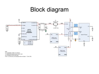
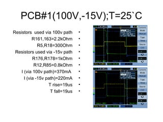
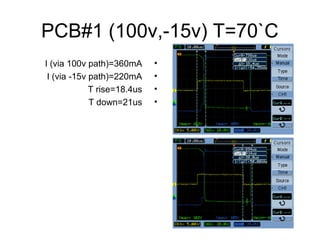
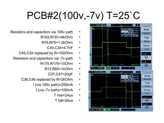
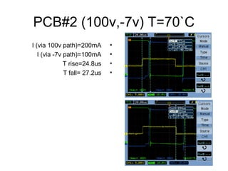
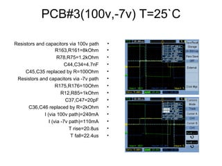
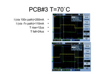


This document summarizes the testing of three printed circuit boards (PCBs) for a switch driver at different temperatures. The switch driver switches between 100V and -7V/-15V voltages at a frequency of 2.5 kHz. Testing was done at room temperature (25°C) and elevated temperature (70°C). Current draw and rise/fall times were measured for the different voltage paths on each PCB. Minor variations were observed between temperatures but all measurements were within specifications. Notes are provided on the function of feedback circuits and proper connection of input signals.


