Project’s goal
•Download as PPTX, PDF•
0 likes•134 views

This document describes the design, testing, and implementation of a switch driver circuit for a cellular signal blocking system. The author redesigned an existing switch driver board that was malfunctioning due to overheating transistors. Through testing and redesign, the author optimized the switch time and removed current spikes and interruptions. The improved switch driver board successfully switched voltages at 2.5 kHz and was integrated into the full system, which then passed all tests and was demonstrated to clients.

Recommended
Recommended
More Related Content
What's hot
What's hot (18)
Viewers also liked
Viewers also liked (20)
Similar to Project’s goal
Similar to Project’s goal (20)
Project’s goal
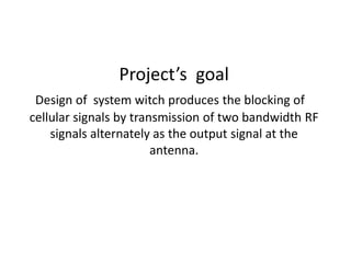
- 1. Project’s goal Design of system witch produces the blocking of cellular signals by transmission of two bandwidth RF signals alternately as the output signal at the antenna.
- 2. My part of project My part of project was testing , debugging and redesign of the existed switch driver witch was the trouble unit of the whole system. I joined the project at the middle when RF switch board was already prepared but it didn’t operate. The transistors on the board was burned due to the excessively high currents flowed through them. During my work by testing and redesign of the switch board I succeeded to achieve the nice performance of the circuit witch switched on frequency=2.5 kHz and more between 100v and -7v. The board was successively integrated as the part of the whole system , passed all tests and the system was sent to U.S.A and presented successfully to client as a demo unit.
- 3. Solved problems 1) Removing of current spikes witch appeared during switch operation 2) Improvement and optimization of switch time. 3) Removing of interruption in RF switch unit caused by driver power dripping up to 10 MHz by involving HPF into switch board. 4) Integrating and operating of the whole system as one unit until getting the required results. 5) Power consumption optimization. 6)Documentation of the design process ,tests and changes were made.
- 4. The function of switch driver •Switching on/off between two diodes in RF block •Switching is made between 100V to -7V/-15V voltage value •Switching frequency is 2.5 kHz
- 8. Checking of driver Three PCB’s of driver were checked under temperature of the room (25`C) and also under temperature of 70`C
- 9. PCB#1(100V,-15V);T=25`C •Resistors used via 100v path •R161,163=2.2kOhm •R5,R18=300Ohm •Resistors used via -15v path •R176,R178=1kOhm •R12,R85=0.8kOhm •I (via 100v path)=370mA •I (via -15v path)=220mA •T rise=19us •T fall=19us
- 10. PCB#1(100V,-15V);T=25`C •Resistors used via 100v path •R161,163=2.2kOhm •R5,R18=300Ohm •Resistors used via -15v path •R176,R178=1kOhm •R12,R85=0.8kOhm •I (via 100v path)=370mA •I (via -15v path)=220mA •T rise=19us •T fall=19us
- 11. PCB#1 (100v,-15v) T=70`C •I (via 100v path)=360mA •I (via -15v path)=220mA •T rise=18.4us •T down=21us
- 12. PCB#2(100v,-7v) T=25`C •Resistors and capacitors via 100v path •R163,R161=8kOhm •R78,R75=1.2kOhm •C44,C34=4.7nF •C45,C35 replaced by R=100Ohm •Resistors and capacitors via -7v path •R175,R176=10Ohm •R12,R85=1kOhm •C37,C47=20pF •C36,C46 replaced by R=2kOhm •I (via 100v path)=200mA •I (via -7v path)=100mA •T rise=24us •T fall=24us
- 13. PCB#2(100v,-7v) T=25`C •Resistors and capacitors via 100v path •R163,R161=8kOhm •R78,R75=1.2kOhm •C44,C34=4.7nF •C45,C35 replaced by R=100Ohm •Resistors and capacitors via -7v path •R175,R176=10Ohm •R12,R85=1kOhm •C37,C47=20pF •C36,C46 replaced by R=2kOhm •I (via 100v path)=200mA •I (via -7v path)=100mA •T rise=24us •T fall=24us
- 14. PCB#2 (100v,-7v) T=70`C •I (via 100v path)=200mA •I (via -7v path)=100mA •T rise=24.8us •T fall= 27.2us
- 15. PCB#3(100v,-7v) T=25`C •R163,R161=8kOhm •R78,R75=1.2kOhm •C44,C34=4.7nF •C45,C35 replaced by R=100Ohm •Resistors and capacitors via -7v path •R175,R176=10Ohm •R12,R85=1kOhm •C37,C47=20pF •C36,C46 replaced by R=2kOhm •I (via 100v path)=240mA •I (via -7v path)=110mA •T rise=20.8us •T fall=22.4us •Resistors and capacitors via 100v path
- 16. PCB#3 T=70`C •I (via 100v path)=250mA •I (via -7v path)=110mA •T rise=12us •T fall=24us
- 17. Attentions and notes •The time delay is caused during of feedback circuit that prevents spikes of high current to appear witch provides to the driver much more stability and defense •The Switch signal input should be connected to the driver just after all other inputs are connected ;that because of feature of HV supply and circuit logic
Editor's Notes
- Igning