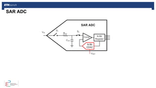
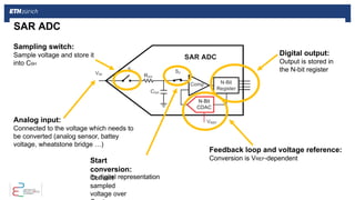
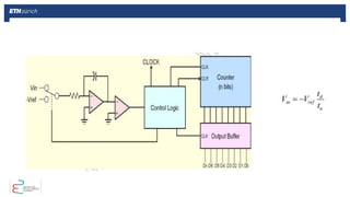
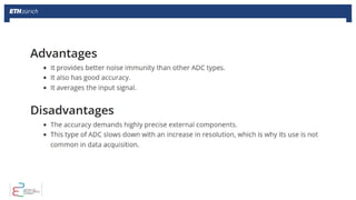
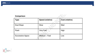
SAR ADC
Digital output:
Outputis stored in
the N-bit register
Sampling switch:
Sample voltage and store it
into CSH
Analog input:
Connected to the voltage which needs to
be converted (analog sensor, battey
voltage, wheatstone bridge …)
Start
conversion:
Convert
sampled
voltage over
Feedback loop and voltage reference:
Conversion is VREF-dependent
its digital representation
7.
| |
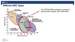
SAR ADCSTM32U585xx – Architecture
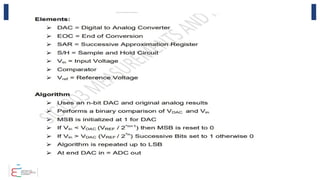
Successive approximation ADC (SAR-ADC)
Converts analog voltage into a digital
representation (Vref dependent).
ADC input selection
over multiplexer
Multiple ADC
channels per
SAR-ADC.
Analog voltage domain and reference voltage
VDDA powers the analog domain. The voltage
needs to stable for precise conversions.
Vref builds the reference voltage for the ADC
conversion.
Calibration registers
ADC needs to be calibrated for precise
measurements.
ADC trigger
Software and
hardware
trigger
available.
Control the start of
a conversion.
8.
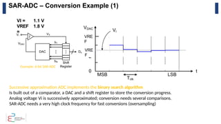
SAR-ADC – ConversionExample (1)
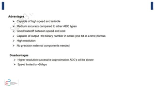
Successive approximation ADC implements the binary search algorithm
Is built out of a comparator, a DAC and a shift register to store the conversion progress.
Analog voltage Vi is successively approximated; conversion needs several comparisons.
SAR-ADC needs a very high clock frequency for fast conversions (oversampling)
Example: 6-bit SAR-ADC
VRE
F
VRE
F
VI =
VREF
=
1.1 V
1.8 V
9.
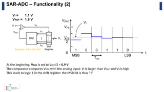
SAR-ADC – Functionality(2)
At the beginning, VDAC is set to VREF/2 = 0.9 V
The comparator compares VDAC with the analog input: Vi is larger than VDAC and VX is high
This leads to logic 1 in the shift register: the MSB bit is thus “1”
Example: 6-bit SAR-ADC
Vi =
VREF =
1.1 V
1.8 V
10.
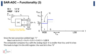
SAR-ADC – Functionality(3)
Since the last conversion yielded logic “1”
VDAC is set to VFS/2 + VFS/4 = 0.9 V + 0.45 V = 1.35 V
The comparator compares VDAC with the analog input: Vi is smaller than VDAC and VX is low
This leads to logic 0 in the shift register: the next bit is thus “0”
Example: 6-bit SAR-ADC
Example: 6-bit SAR-ADC
VI =
VREF
=
1.1 V
1.8 V
11.
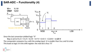
SAR-ADC – Functionality(4)
Since the last conversion yielded logic “0”
VDAC is set to VFS/2 + VFS/4 - VFS/8 = 0.9 V + 0.45 V – 0.225V = 1.125 V
The comparator compares VDAC with the analog input: Vi is smaller than VDAC and VX is low
This leads to logic 0 in the shift register: the next bit is thus “0”
Example: 6-bit SAR-ADC
VI =
VREF
=
1.1 V
1.8 V
12.
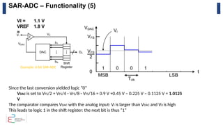
SAR-ADC – Functionality(5)
Since the last conversion yielded logic “0”
VDAC is set to VFS/2 + VFS/4 - VFS/8 - VFS/16 = 0.9 V +0.45 V – 0.225 V – 0.1125 V = 1.0125
V
The comparator compares VDAC with the analog input: Vi is larger than VDAC and VX is high
This leads to logic 1 in the shift register: the next bit is thus “1”
Example: 6-bit SAR-ADC
VI =
VREF
=
1.1 V
1.8 V
13.
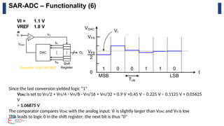
SAR-ADC – Functionality(6)
Since the last conversion yielded logic “1”
VDAC is set to VFS/2 + VFS/4 - VFS/8 - VFS/16 + VFS/32 = 0.9 V +0.45 V – 0.225 V – 0.1125 V + 0.05625
V
= 1.06875 V
The comparator compares VDAC with the analog input: Vi is slightly larger than VDAC and VX is low
This leads to logic 0 in the shift register: the next bit is thus “0”
Example: 6-bit SAR-ADC
VI =
VREF
=
1.1 V
1.8 V
14.
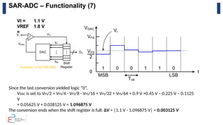
SAR-ADC – Functionality(7)
Since the last conversion yielded logic “0”,
VDAC is set to VFS/2 + VFS/4 - VFS/8 - VFS/16 + VFS/32 + VFS/64 = 0.9 V +0.45 V – 0.225 V – 0.1125
V
+ 0.05625 V + 0.028125 V = 1.096875 V
The conversion ends when the shift register is full: ΔV = |1.1 V - 1.096875 V| = 0.003125 V
Example: 6-bit SAR-ADC
VI =
VREF
=
1.1 V
1.8 V
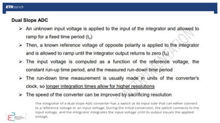
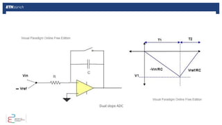
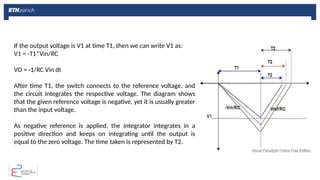
If the outputvoltage is V1 at time T1, then we can write V1 as:
V1 = -T1*Vin/RC
VO = -1/RC Vin dt
After time T1, the switch connects to the reference voltage, and
the circuit integrates the respective voltage. The diagram shows
that the given reference voltage is negative, yet it is usually greater
than the input voltage.
As negative reference is applied, the integrator integrates in a
positive direction and keeps on integrating until the output is
equal to the zero voltage. The time taken is represented by T2.
22.
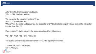
After time T1,the integrator’s output is:
VO = -1 / RC -Vref dt + Vinitial
We can write the equation for time T2 as:
VO = -T2 * (-Vref) / RC + V1
Where V1 is the initial voltage across the capacitor and VO is the total output voltage across the integrator
in total time T1 + T2.
If we replace V1 by its value in the above equation, then it becomes:
VO = T2 * (Vref) / RC + (-T1 * Vin / RC)
The output would be equal to zero after T1+T2. The equation becomes:
T2*(Vref)/RC +(-T1*Vin/RC)=0
T2=T1*Vin/Vref


![Interfacing technique with 8085- ADC[0808]](https://cdn.slidesharecdn.com/ss_thumbnails/adc-160307140900-thumbnail.jpg?width=640&height=640&fit=bounds)


