1
V
V
L
L
S
S
I
I
T
T
E
E
C
C
H
H
N
N
O
O
L
L
O
O
G
G
Y
Y
CHIP
CHIP DESIGN
DESIGN
FET ARRAY DESIGN-STICK DIAGRAMS
2
V
V
L
L
S
S
I
I
T
T
E
E
C
C
H
H
N
N
O
O
L
L
O
O
G
G
Y
Y
CHIP
CHIP DESIGN
DESIGN
FET Array Design – Stick Diagrams
Basics/History
3
V
V
L
L
S
S
I
I
T
T
E
E
C
C
H
H
N
N
O
O
L
L
O
O
G
G
Y
Y
CHIP
CHIP DESIGN
DESIGN
FET Array Design – Stick Diagrams
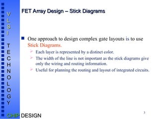
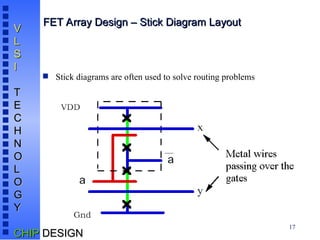
 One approach to design complex gate layouts is to use
Stick Diagrams.
 Each layer is represented by a distinct color.
 The width of the line is not important as the stick diagrams give
only the wiring and routing information.
 Useful for planning the routing and layout of integrated circuits.
4
V
V
L
L
S
S
I
I
T
T
E
E
C
C
H
H
N
N
O
O
L
L
O
O
G
G
Y
Y
CHIP
CHIP DESIGN
DESIGN
FET Array Design – Stick Diagrams
 Commonly used stick diagrams colors are :
 Polysilicon (gates) = red
 Doped n+ / p+ (active) = green
 N-well either by ----- (dashed line) or yellow
 Metal1 = blue
 Metal 2= gray
 Contacts = Black X
5
V
V
L
L
S
S
I
I
T
T
E
E
C
C
H
H
N
N
O
O
L
L
O
O
G
G
Y
Y
CHIP
CHIP DESIGN
DESIGN
FET Array Design – Stick Diagrams
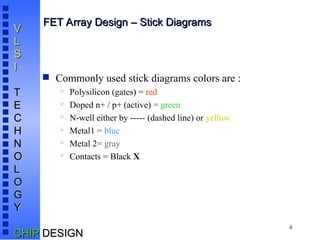
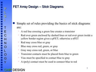
 Simple set of rules providing the basics of stick diagrams
are:
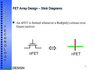
 A red line crossing a green line creates a transistor
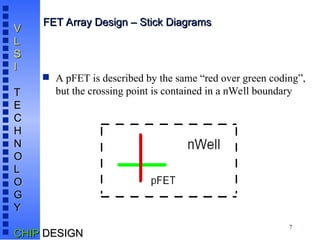
 Red over green enclosed by dashed lines or red over green inside a
yellow border region gives a pFET; otherwise a nFET
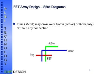
 Red may cross blue or gray
 Blue may cross red, green, or gray
 Gray may cross red, green, or blue
 Transistor contacts must be placed from blue to green
 Vias must be specified to contact blue to gray
 A (poly) contact must be used to connect blue to red
6
V
V
L
L
S
S
I
I
T
T
E
E
C
C
H
H
N
N
O
O
L
L
O
O
G
G
Y
Y
CHIP
CHIP DESIGN
DESIGN
FET Array Design – Stick Diagrams
 An nFET is formed whenever a Red(poly) crosses over
Green (active)
7
V
V
L
L
S
S
I
I
T
T
E
E
C
C
H
H
N
N
O
O
L
L
O
O
G
G
Y
Y
CHIP
CHIP DESIGN
DESIGN
FET Array Design – Stick Diagrams
 A pFET is described by the same “red over green coding”,
but the crossing point is contained in a nWell boundary
8
V
V
L
L
S
S
I
I
T
T
E
E
C
C
H
H
N
N
O
O
L
L
O
O
G
G
Y
Y
CHIP
CHIP DESIGN
DESIGN
FET Array Design – Stick Diagrams
 Blue (Metal) may cross over Green (active) or Red (poly)
without any connection
9
V
V
L
L
S
S
I
I
T
T
E
E
C
C
H
H
N
N
O
O
L
L
O
O
G
G
Y
Y
CHIP
CHIP DESIGN
DESIGN
FET Array Design – Stick Diagrams
 Connections between layers are specified as X. Consider
the Example of nFET. In this layout,
 Poly contact: Metal1-to-Poly
 Active contact: Metal1-to-Active
10
V
V
L
L
S
S
I
I
T
T
E
E
C
C
H
H
N
N
O
O
L
L
O
O
G
G
Y
Y
CHIP
CHIP DESIGN
DESIGN
FET Array Design – Stick Diagrams
 Metal lines on different layers can cross one another.
Contacting two metal lines requires a via
11
V
V
L
L
S
S
I
I
T
T
E
E
C
C
H
H
N
N
O
O
L
L
O
O
G
G
Y
Y
CHIP
CHIP DESIGN
DESIGN
To create CMOS gates
 To Create CMOS gates,
 VDD is represented as,
 VSS is represented as,
12
V
V
L
L
S
S
I
I
T
T
E
E
C
C
H
H
N
N
O
O
L
L
O
O
G
G
Y
Y
CHIP
CHIP DESIGN
DESIGN
FET Array Design – Stick Diagrams
 Consider the example of a NOT gate as shown below
13
V
V
L
L
S
S
I
I
T
T
E
E
C
C
H
H
N
N
O
O
L
L
O
O
G
G
Y
Y
CHIP
CHIP DESIGN
DESIGN
FET Array Design – Stick Diagrams
 Inverter layout is given as shown below,
14
V
V
L
L
S
S
I
I
T
T
E
E
C
C
H
H
N
N
O
O
L
L
O
O
G
G
Y
Y
CHIP
CHIP DESIGN
DESIGN
FET Array Design – Stick Diagram
 Alternate Inverter Layout,
x
x
15
V
V
L
L
S
S
I
I
T
T
E
E
C
C
H
H
N
N
O
O
L
L
O
O
G
G
Y
Y
CHIP
CHIP DESIGN
DESIGN
FET Array Design – Stick Diagrams
 Transmission Gates. The symbol and circuit of a transmission gate is as
shown below.
16
V
V
L
L
S
S
I
I
T
T
E
E
C
C
H
H
N
N
O
O
L
L
O
O
G
G
Y
Y
CHIP
CHIP DESIGN
DESIGN
FET Array Design – Stick Diagrams
 The stick diagram layout for a transmission gate is as shown below.
17
V
V
L
L
S
S
I
I
T
T
E
E
C
C
H
H
N
N
O
O
L
L
O
O
G
G
Y
Y
CHIP
CHIP DESIGN
DESIGN
FET Array Design – Stick Diagram Layout
 Stick diagrams are often used to solve routing problems
18
V
V
L
L
S
S
I
I
T
T
E
E
C
C
H
H
N
N
O
O
L
L
O
O
G
G
Y
Y
CHIP
CHIP DESIGN
DESIGN
FET Array Design – Stick Diagrams
 Uses:
 Provides easy approach to performing simple CMOS circuit
layouts
 Helps in planning physical design before using the actual CAD
tool
 Complicated wiring of gates and cells is often easier to visualize
using stick diagrams
 Crossovers (such as Metal1-Metal2) are easy to plan using stick
diagrams
 Helps in visualizing the signal flow in complex networks
19
V
V
L
L
S
S
I
I
T
T
E
E
C
C
H
H
N
N
O
O
L
L
O
O
G
G
Y
Y
CHIP
CHIP DESIGN
DESIGN
FET Array Design – Stick Diagrams
 References:
 Introduction to VLSI Circuits and Systems, by John P.Uyemura
 Physical Design of CMOS Integrated Circuits, by John P.Uyemura
 Basic VLSI Design – Principles and Applications, by D.A.Pucknell and
K.Eshraghain
 http://www.personal.dundee.ac.uk/~dmgoldie/teaching/eg4013/lectures/10
 http://www.microlab.ch/academics/courses/cbt/cbt-vlsi/layers_repres.html
 http://www.stanford.edu/class/ee271/stick_to_layout/stick_to_layout.html
20
V
V
L
L
S
S
I
I
T
T
E
E
C
C
H
H
N
N
O
O
L
L
O
O
G
G
Y
Y
CHIP
CHIP DESIGN
DESIGN
Thank you…
Thank you…

FET ARRAY DESIGN - STICK DIAGRAMS presentation