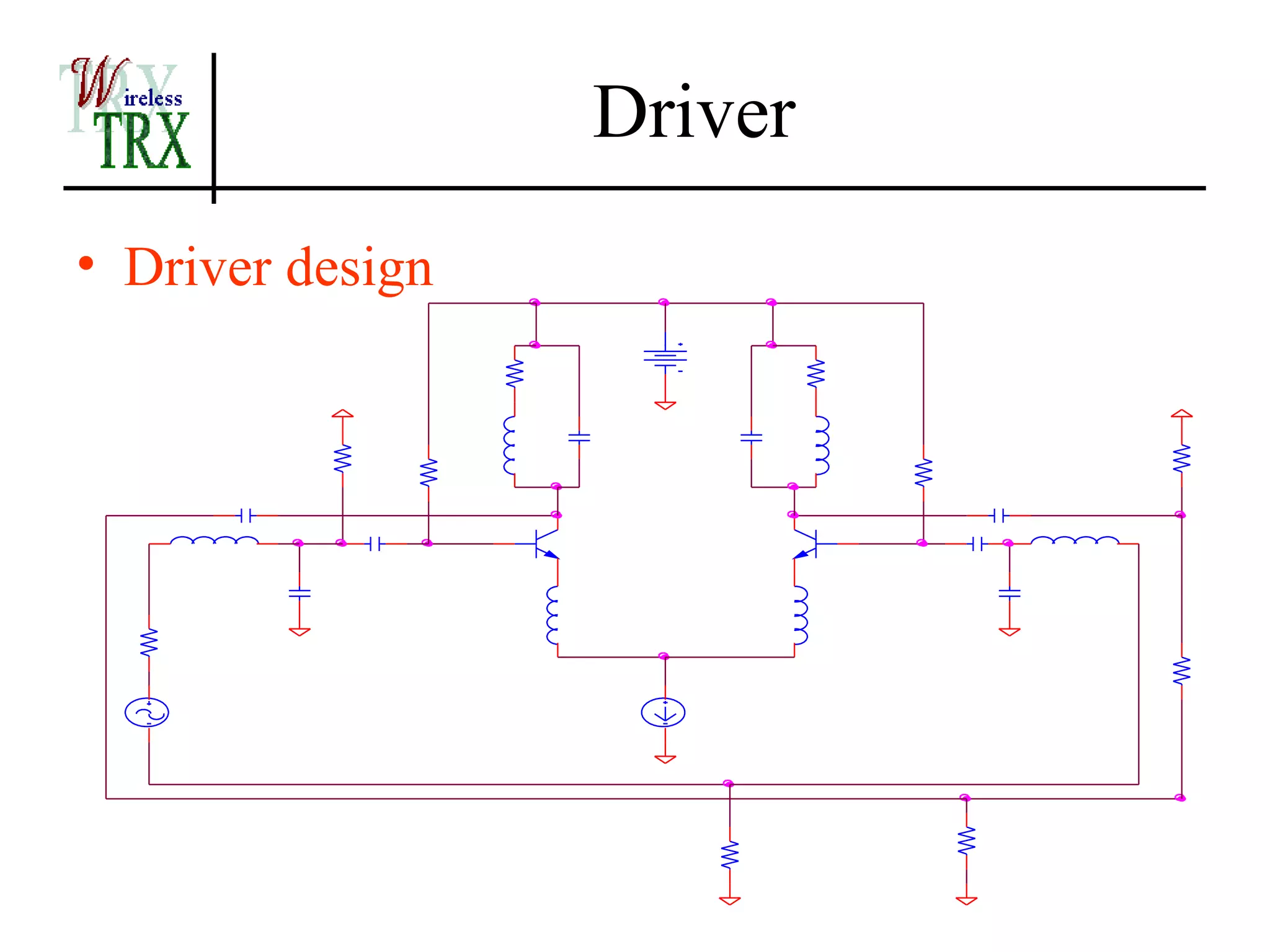
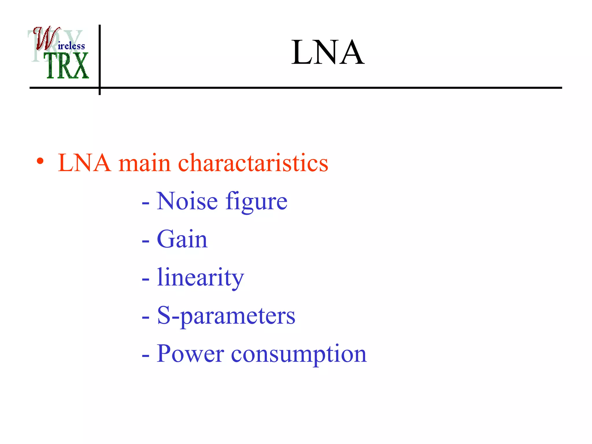
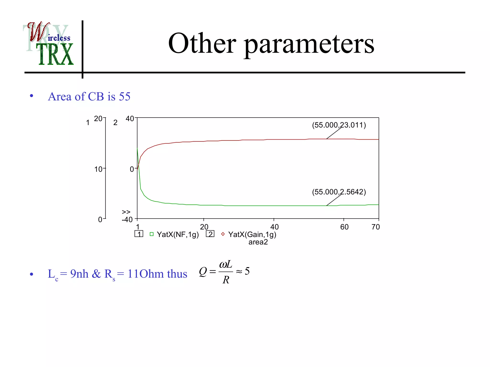
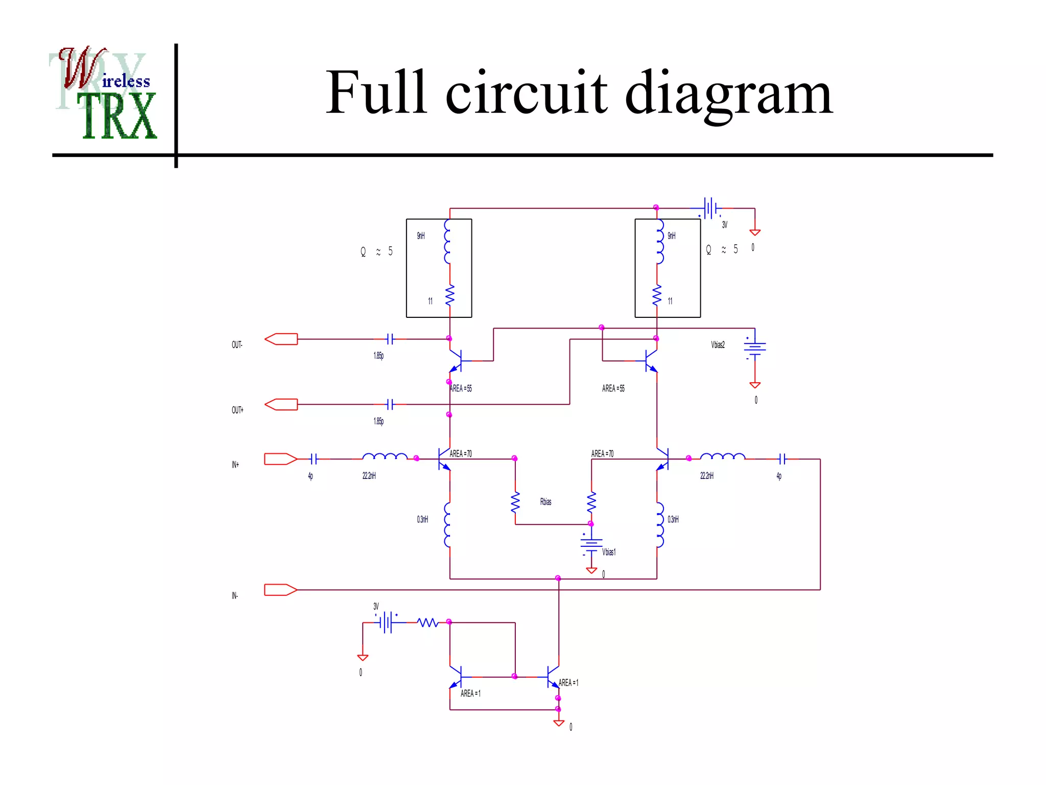
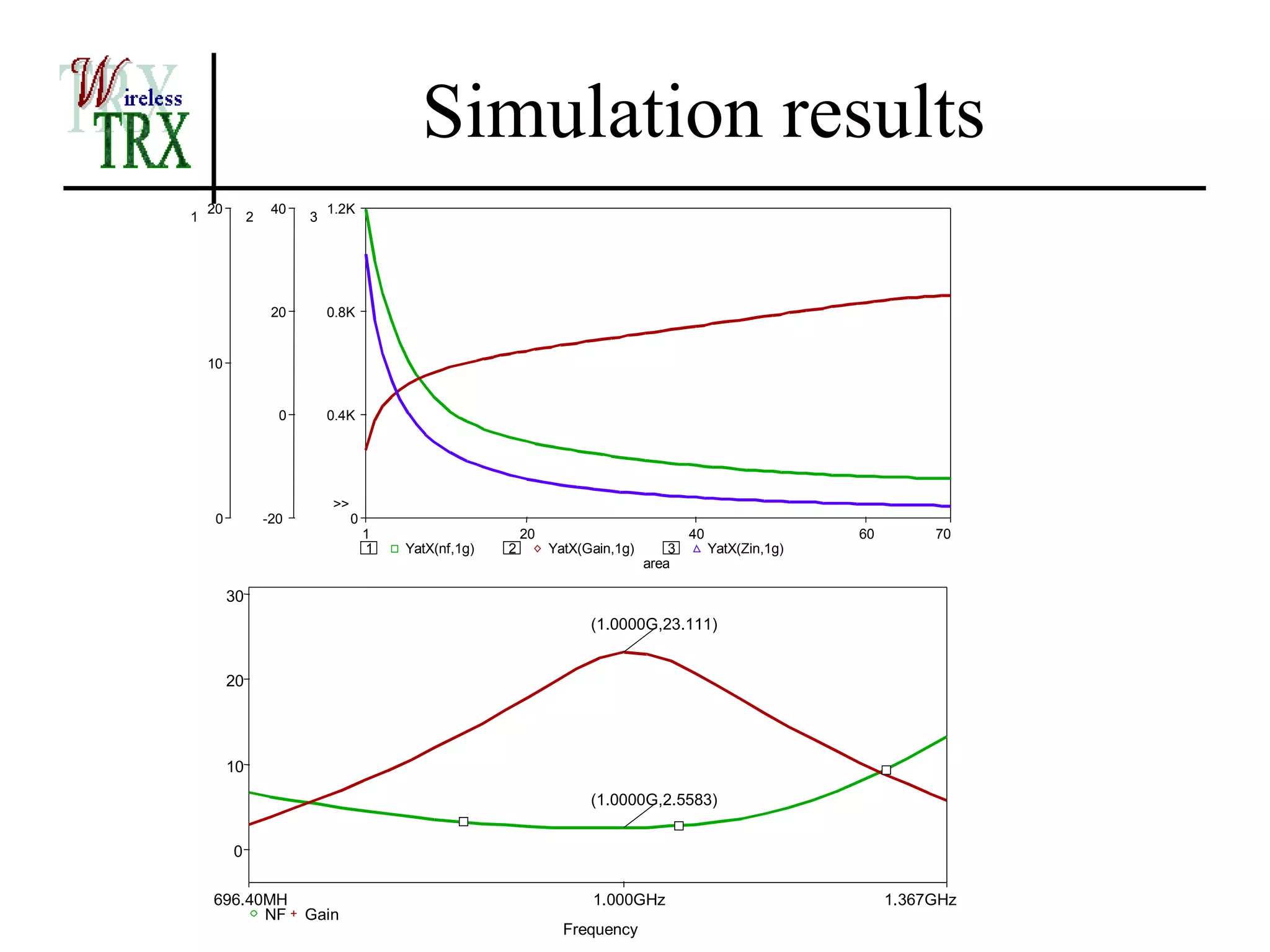
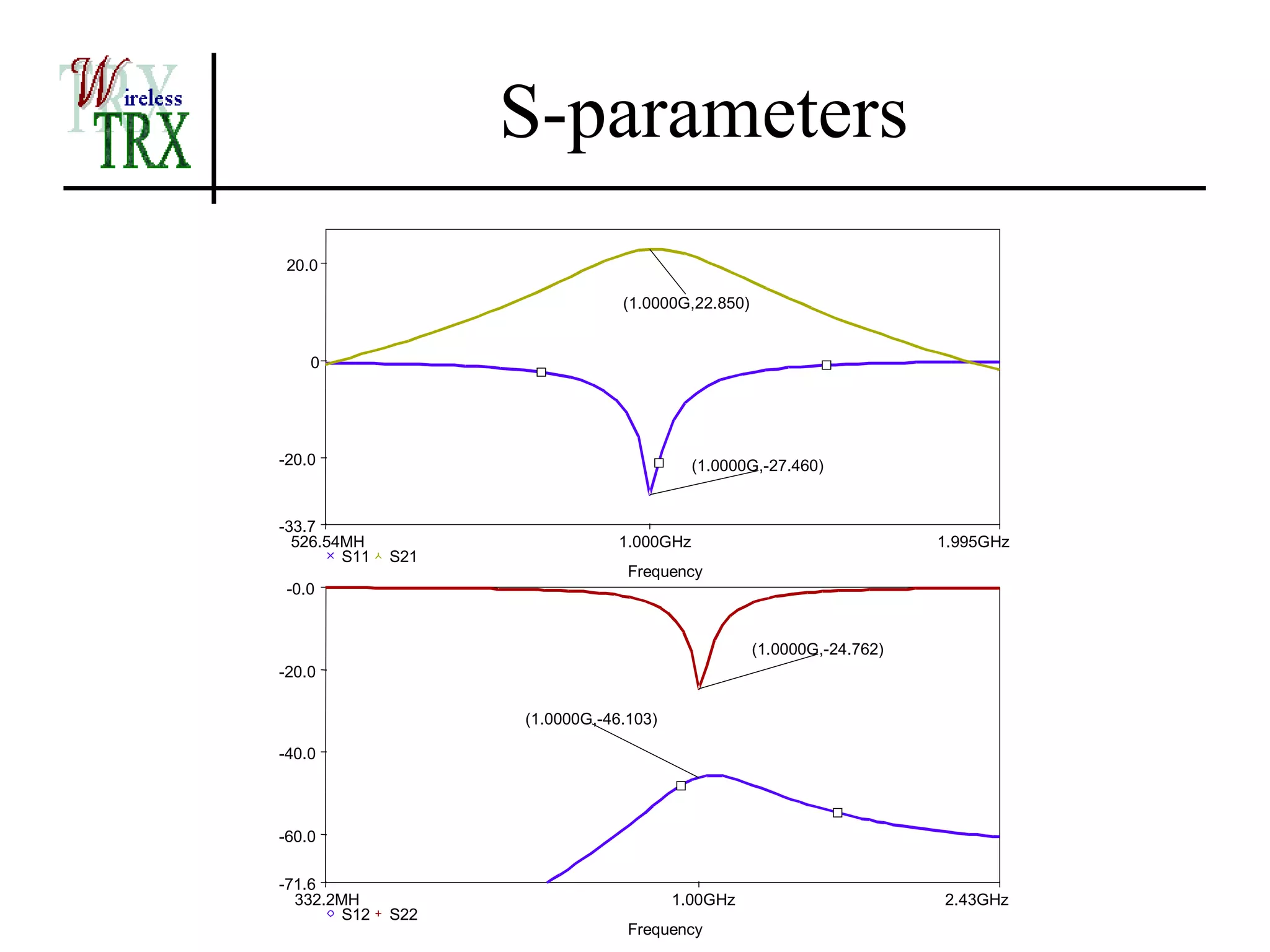
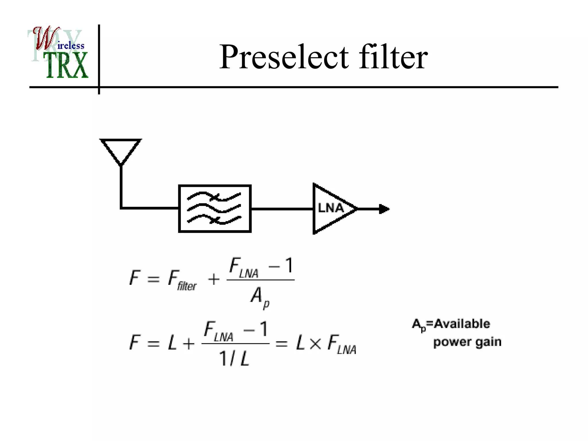
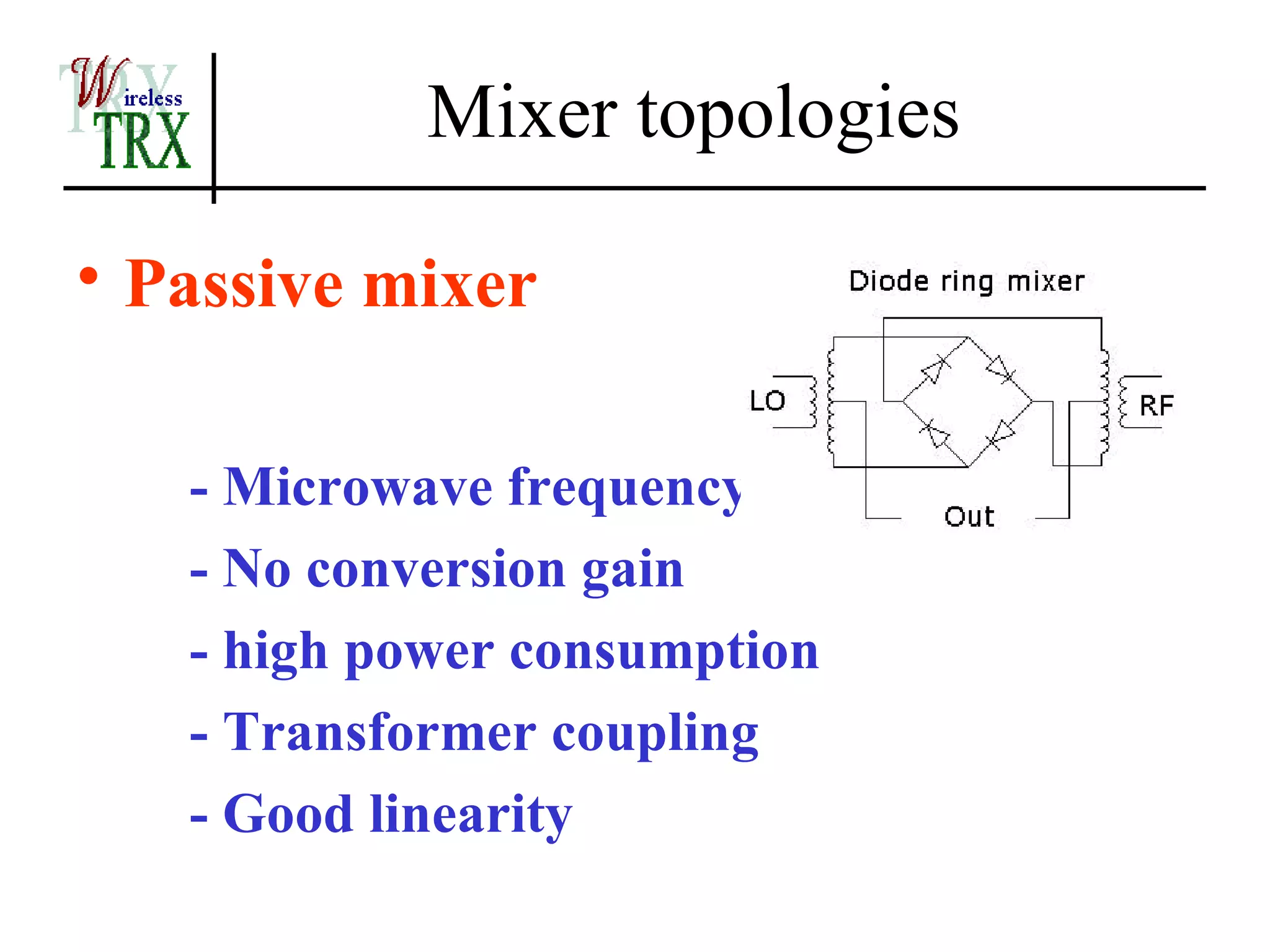
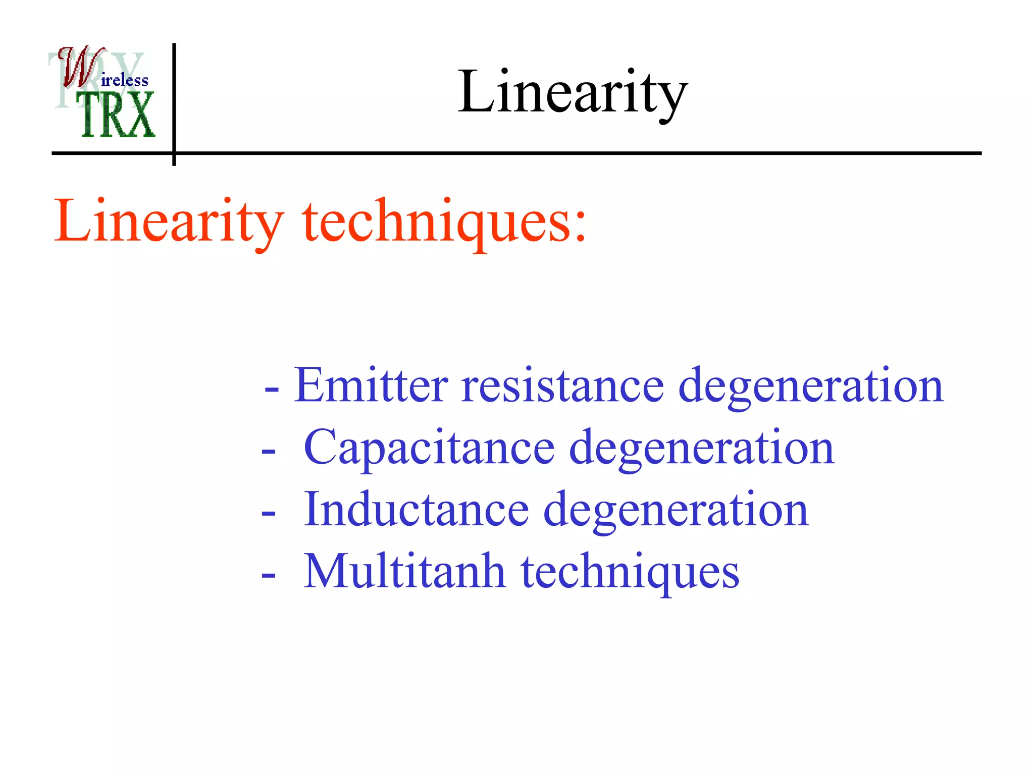
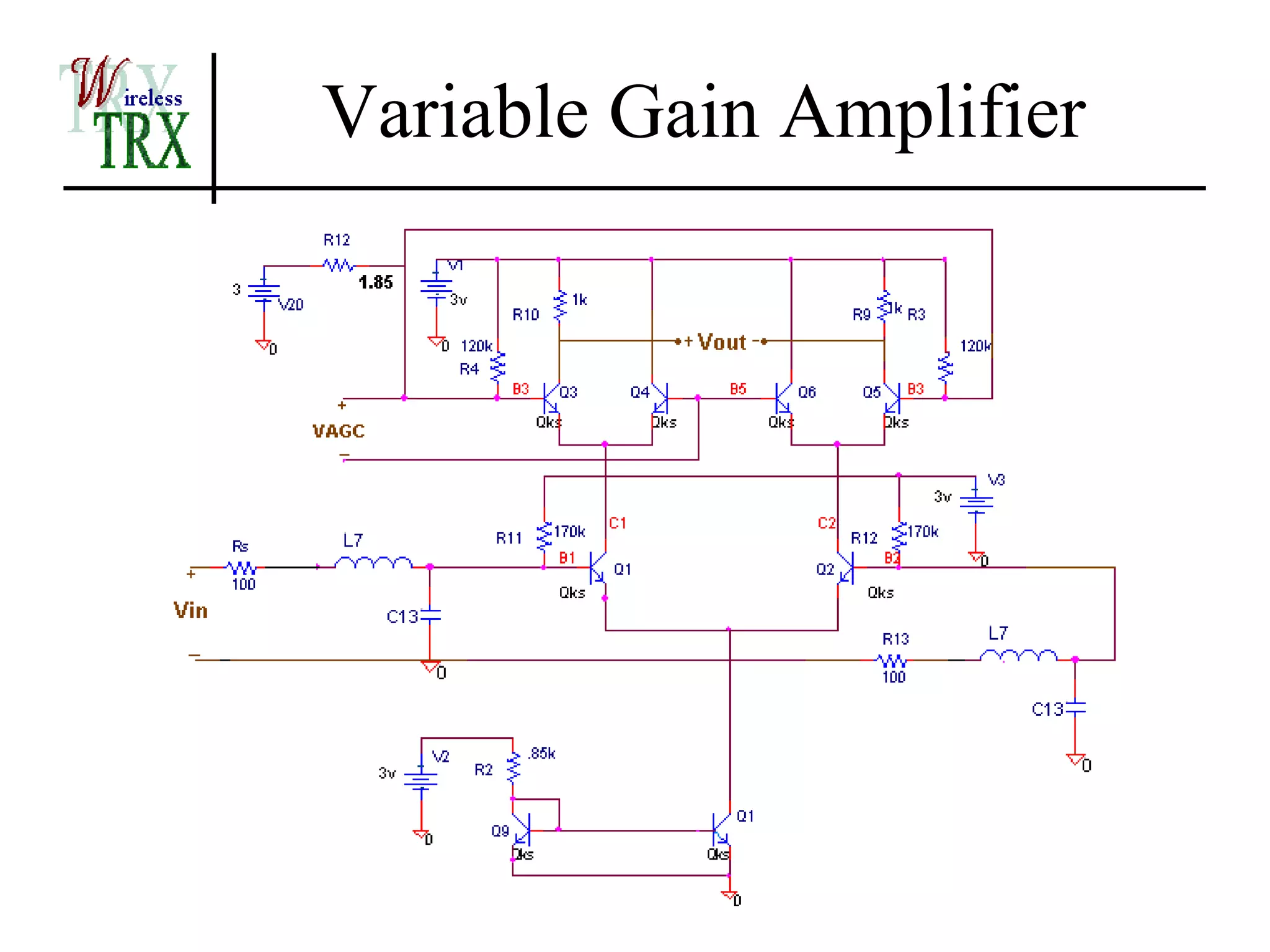
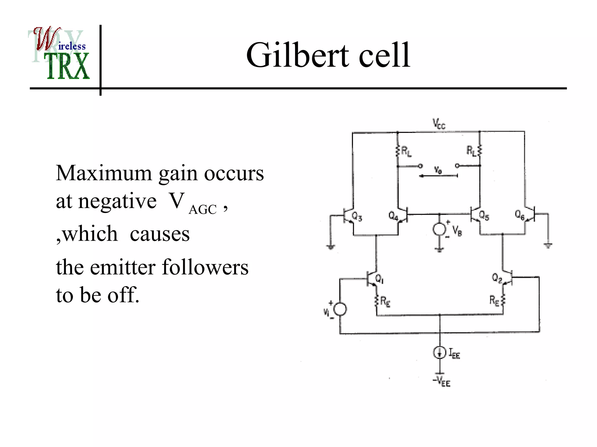
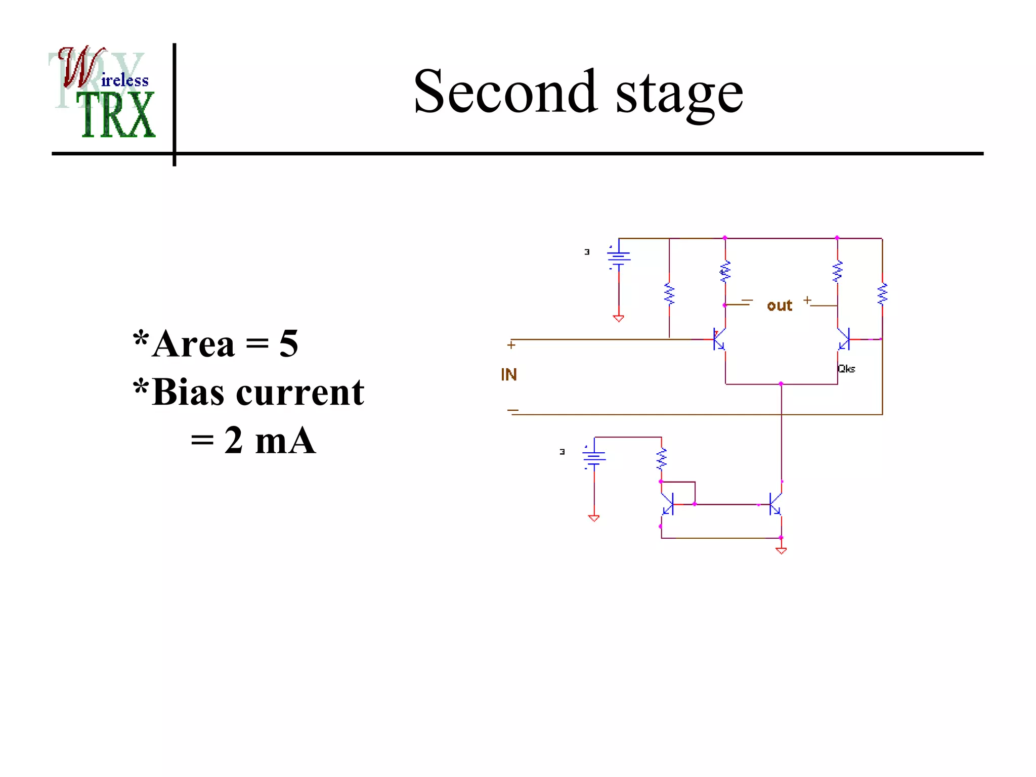
Here are the key steps to design an LNA:
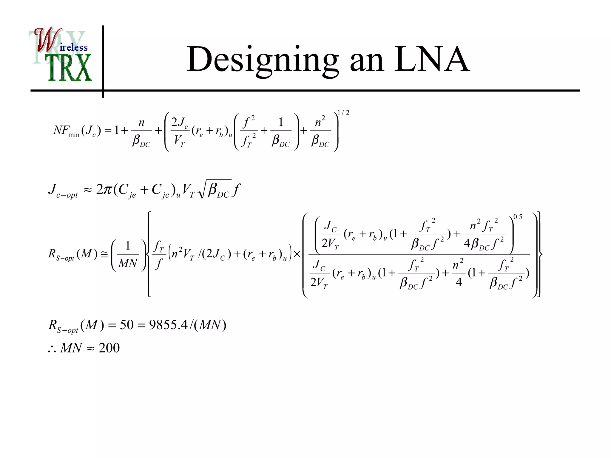
1. Calculate the minimum achievable noise figure NFmin using the noise parameter Fmin. This depends on device parameters like transconductance gm, output resistance ro, bias current density Jc, etc.
2. Choose an optimal value for Jc that minimizes NFmin. This Jc-opt depends on device capacitances, bias voltage, and frequency of operation.
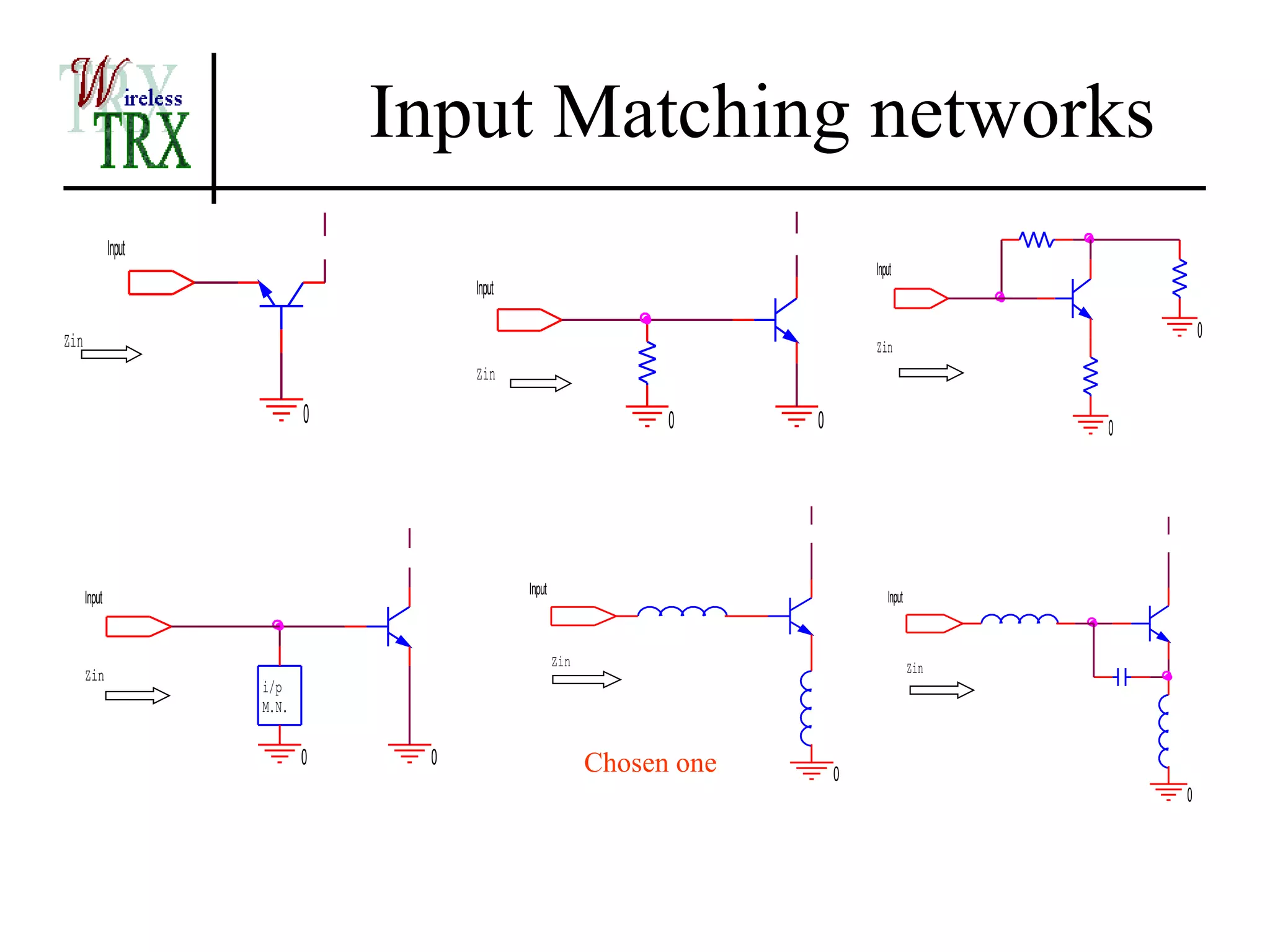
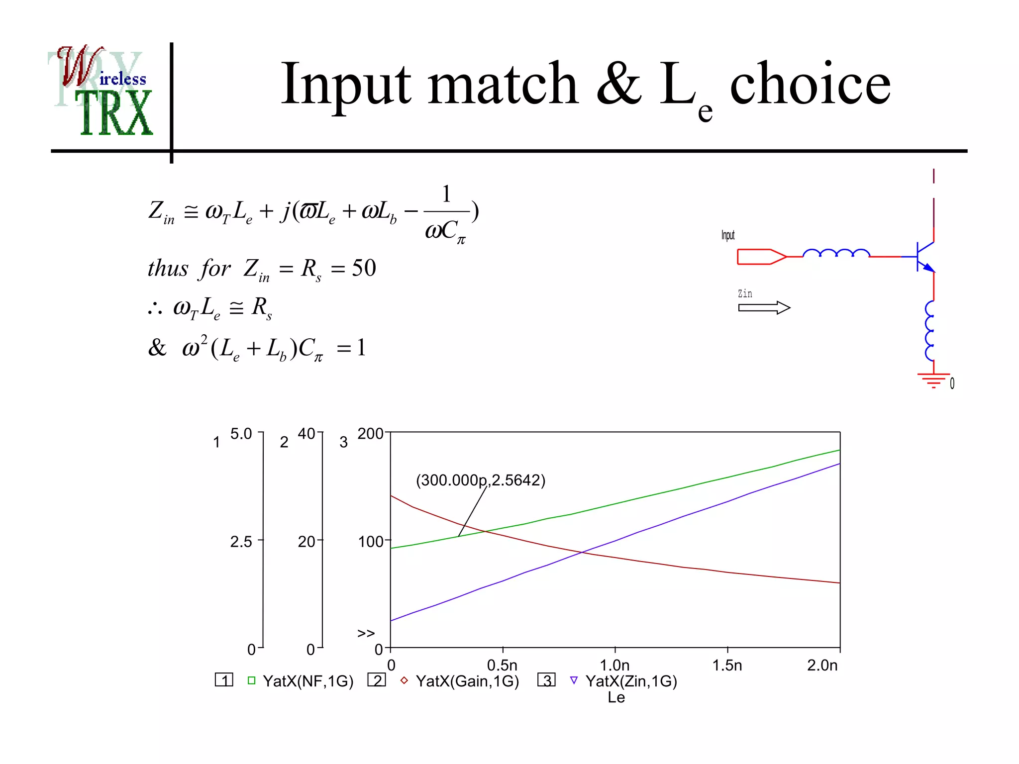
3. Design the input matching network to transform the source impedance (usually 50 ohms) to the optimal impedance looking into the transistor for minimum noise. This involves choosing component values for the matching network.
4. Design the biasing circuitry to provide stable bias point


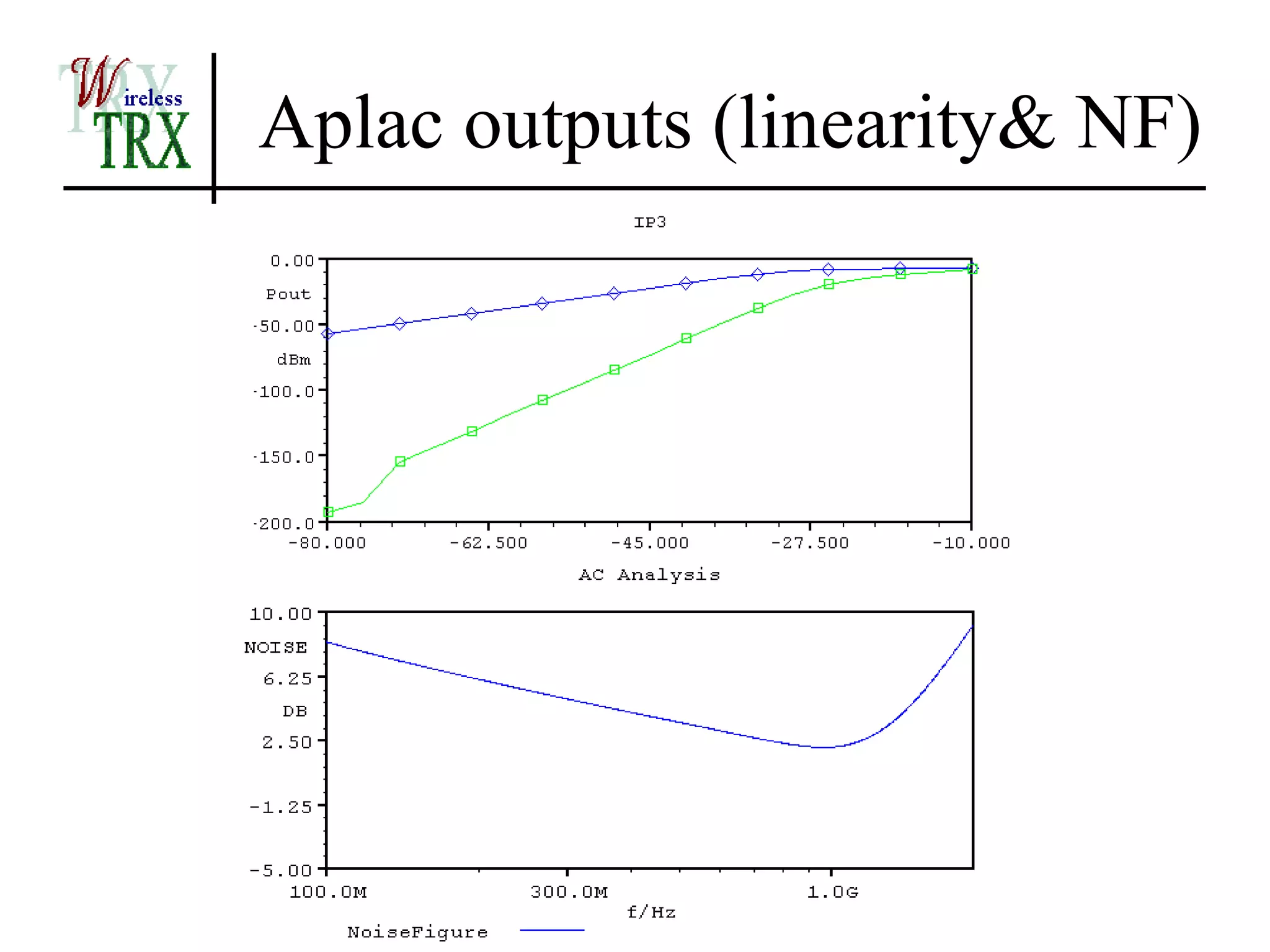
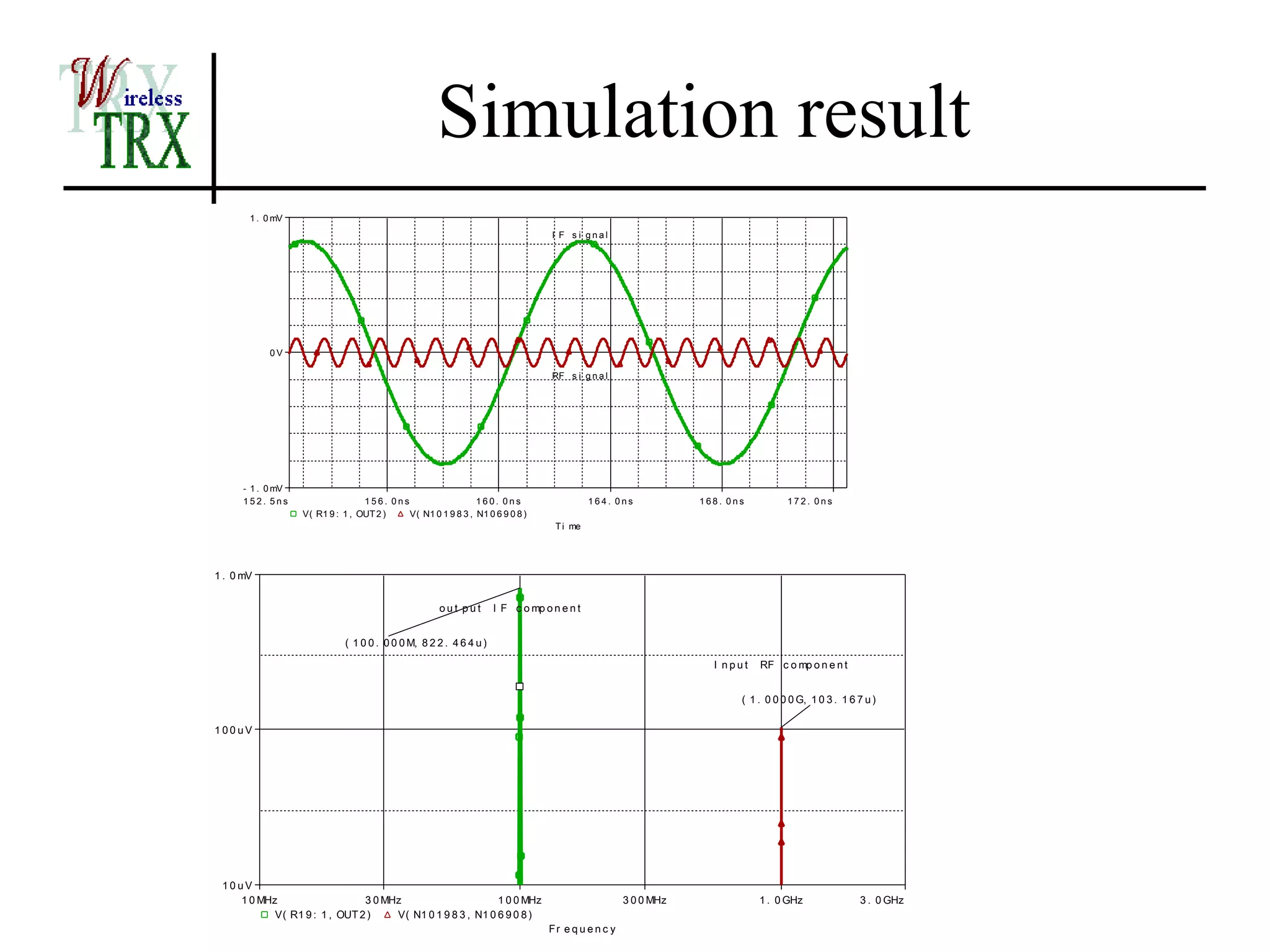
![MWO outputs(linearity &
S-parameters)
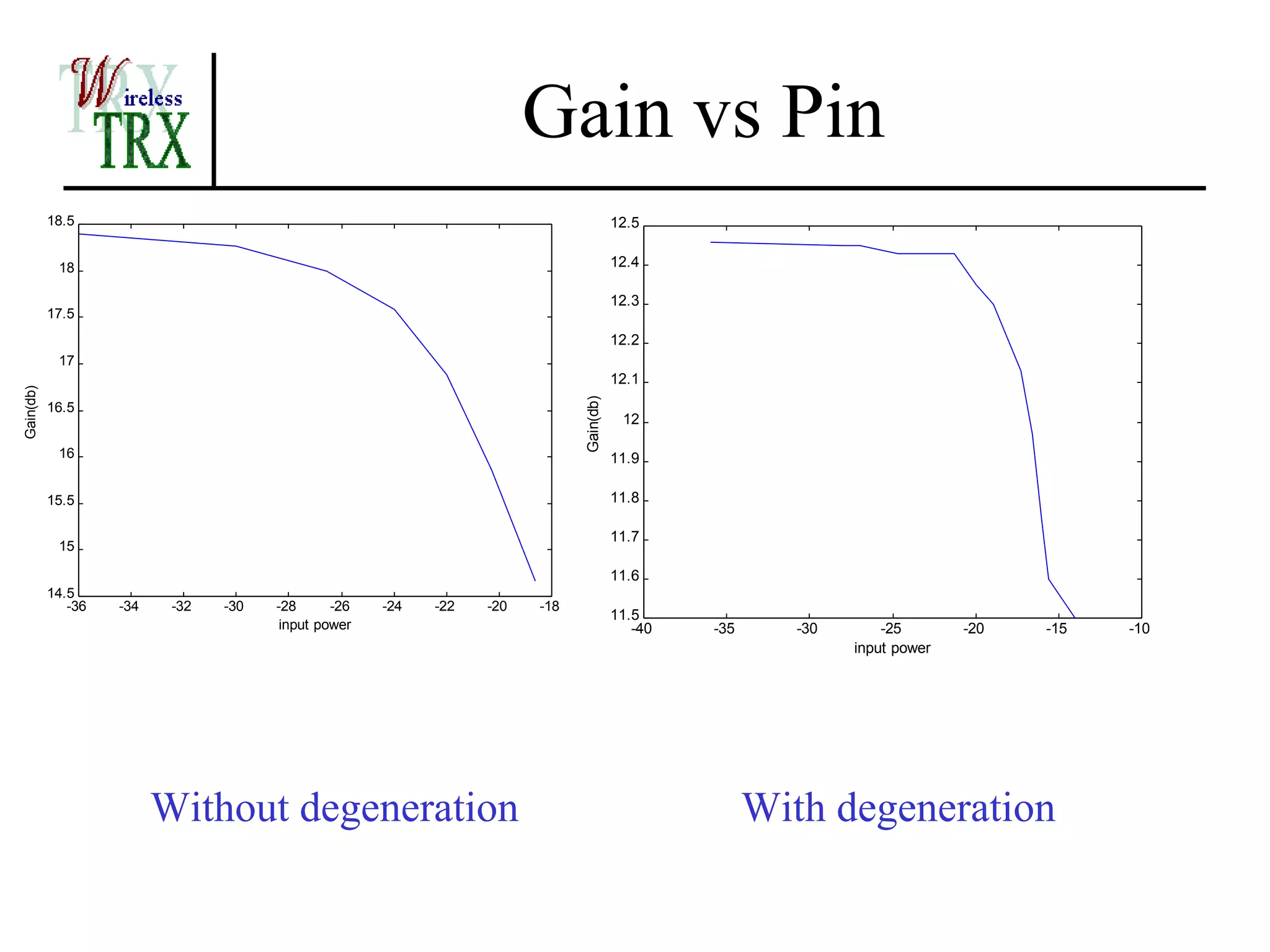
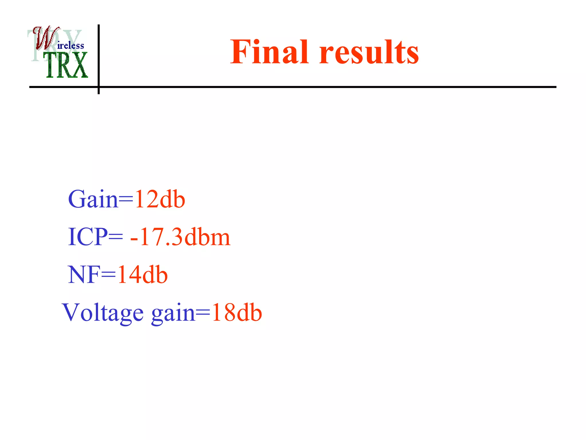
Pout vs Pin
0
-50
IM1_SP[PORT_2,1] (dBm)
Schematic 1
-100 IM3_SP[PORT_2,1] (dBm)
Schematic 1
-150
-60 -50 -40 -30 -20
Power (dBm)
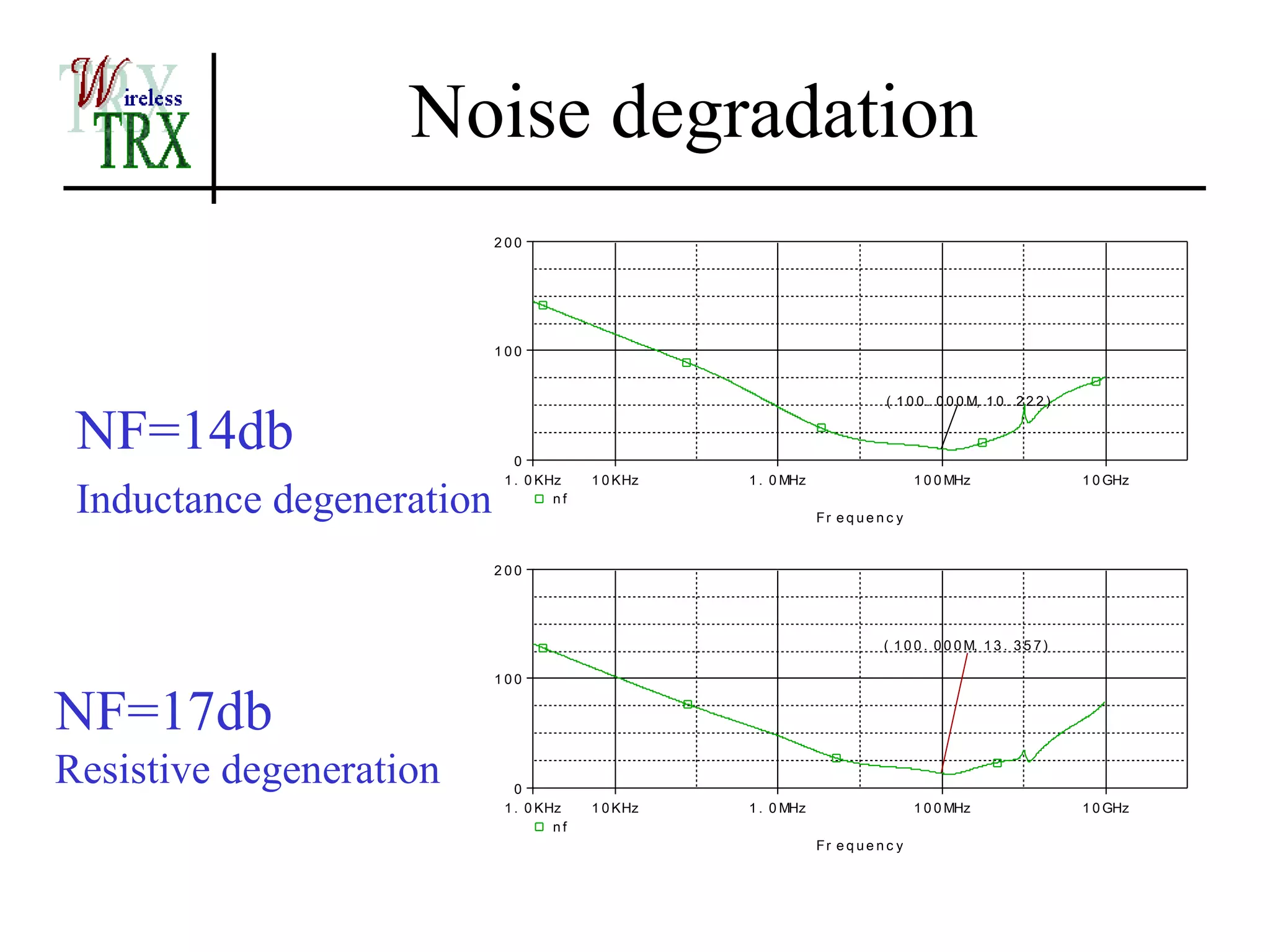
s-parameters
Swp Max
1.0
s param
0.8
1.1GHz
30
6
0.
0
2.
4
0.
0
3.
S[1,1]
0 Schematic 1 4.
0
5.0
0.2 S[2,1]
Schematic 1
10.0
DB(|S[1,1]|) S[1,2]
-30 Schematic 1
Schematic 1
10.0
0.2
0.4
0.6
0.8
1.0
2.0
3.0
4.0
5.0
0
S[2,2]
DB(|S[2,1]|) Schematic 1
Schematic 1 -10.0
-60 2
-0.
DB(|S[1,2]|) 0
-5.
Schematic 1
0 .
-4
.0
-3
.4
-90 DB(|S[2,2]|) -0
Schematic 1
.0
0.9 0.95 1 1.05 1.1
-2
6.
-0
Frequency (GHz)
-0.8
Swp Min
-1.0
0.9GHz](https://image.slidesharecdn.com/project-120614060157-phpapp01/75/Project-52-2048.jpg)


![automatedbricklayout[1]](https://cdn.slidesharecdn.com/ss_thumbnails/649e4693-3c80-404c-bca7-58bbc24e87cd-150721035354-lva1-app6891-thumbnail.jpg?width=640&height=640&fit=bounds)


