Pcb123v4 manual
•
0 likes•234 views

PCB123 Version 4 is a user guide and reference manual for a PCB design software. The software allows users to complete a printed circuit board design from concept to manufacturing within a single program. It features schematic design and PCB layout within the same application, where the schematic and layout are considered two views of the same underlying database, eliminating the need for a separate netlist file. The guide covers getting started, schematic design, PCB layout, and contains reference sections for the schematic editor and layout tools.

More Related Content
What's hot
What's hot (20)
Viewers also liked
Similar to Pcb123v4 manual
Similar to Pcb123v4 manual (20)
Recently uploaded
Recently uploaded (20)
Pcb123v4 manual
- 1. PCB123 Version 4 User Guide and Reference manual Copyright © 2010,
- 2. 1 Contents Overview..........................................................................14 Introduction............................................................................................................................ 14 Software features out of the box .............................................................................................. 14 User Extendibility..................................................................................................................... 16 One eye on the future.............................................................................................................. 16 Our Commitment..................................................................................................................... 17 Part 1 - Getting Started ...................................................20 Introduction ............................................................................................... 21 Screen Layout............................................................................................. 23 Common functionality ................................................................................ 24 Pan and Zoom......................................................................................................................... 24 Names and Numbers ............................................................................................................... 25 Selection ................................................................................................................................ 27 Context Menus ........................................................................................................................ 28 Commands ............................................................................................................................. 28 Starting a New Design................................................................................ 29 Overview of PCB design tasks................................................................................................... 29 Data Requirements.................................................................................................................. 32 The New-Board Wizard ............................................................................................................ 34 Starting Without the New-Board Wizard .................................................................................... 38 Results of Creating a New Design ............................................................................................. 38 Default Settings....................................................................................................................... 39 PCB123 Directories .................................................................................................................. 40 Part 2 - Schematic User Guide.........................................42 The Schematic/PCB Contract ..................................................................... 43 A little background .................................................................................................................. 43 The Design-by-contract solution ............................................................................................... 44 Properties................................................................................................... 46
- 3. 2 Symbols and Parts...................................................................................... 48 Parts ...................................................................................................................................... 50 Symbols ................................................................................................................................. 50 Pre-Defined Parts .................................................................................................................... 62 The Part Taxonomy .................................................................................... 63 Hierarchy and Inheritance........................................................................................................ 64 Pre-defined Parts..................................................................................................................... 67 The Part Manager.................................................................................................................... 69 Acquiring Data ........................................................................................................................ 70 The Symbol Editor ...................................................................................... 74 Inside/Outside ........................................................................................................................ 75 Adding pins............................................................................................................................. 76 Adding Shapes ........................................................................................................................ 78 Adding Arcs ............................................................................................................................ 80 Adding Text ............................................................................................................................ 81 Adding properties.................................................................................................................... 82 Saving symbols ....................................................................................................................... 83 Sections.................................................................................................................................. 83 Binding to specific symbols....................................................................................................... 84 Mapping pin names to pin numbers .......................................................................................... 85 Hidden pins ............................................................................................................................ 85 Saving parts............................................................................................................................ 86 Finding Parts .............................................................................................. 87 Part search ............................................................................................................................. 87 Define New Part ...................................................................................................................... 88 Ports........................................................................................................... 94 Ports and net names................................................................................................................ 94 Schematic Pages ........................................................................................ 96 Adding Schematic Pages .......................................................................................................... 97 Synchronization pages ............................................................................................................. 98 The Title Block ........................................................................................................................ 98 Page size................................................................................................................................ 98
- 4. 3 The Schematic Editor................................................................................ 100 Adding parts to a page........................................................................................................... 100 Adding ports to a page .......................................................................................................... 100 Adding wires......................................................................................................................... 101 Adding nomenclature............................................................................................................. 101 Properties............................................................................................................................. 102 Cut/copy/paste...................................................................................................................... 102 Moving parts......................................................................................................................... 102 Part 3 - Layout User Guide ............................................104 Layout Views and Panels.......................................................................... 105 Display Panel ........................................................................................................................ 105 Design View.......................................................................................................................... 108 3D View................................................................................................................................ 108 Footprint Editor..................................................................................................................... 109 DRC Panel ............................................................................................................................ 109 Project Panel......................................................................................................................... 109 PCB Design Tasks ..................................................................................... 111 Create missing footprints......................................................................... 112 Creating footprints from scratch.............................................................................................. 113 Modify and existing footprint from a library.............................................................................. 113 Use an existing component as a starting point ......................................................................... 113 Prepare Mechanical Features .................................................................................................. 113 Adjusting the board outline .................................................................................................... 113 Add mounting hardware......................................................................................................... 114 Place components .................................................................................... 117 Fixed component locations ..................................................................................................... 117 Autoplace components........................................................................................................... 118 Manual place components ...................................................................................................... 118 Power, ground, and critical routing.......................................................... 118 Power and ground plane layers............................................................................................... 118 Routed power and ground...................................................................................................... 123
- 5. 4 Critical routing ...................................................................................................................... 124 General routing ..................................................................................................................... 124 Fanout and autorouting ......................................................................................................... 125 Manual routing...................................................................................................................... 127 Routing techniques................................................................................................................ 129 Fills, and Nomenclature............................................................................ 130 Active copper fill regions ........................................................................................................ 130 Nomenclature ....................................................................................................................... 132 Order Boards ............................................................................................ 135 The Order process................................................................................................................. 135 Routing your Design................................................................................. 139 Before you route ................................................................................................................... 139 Routing the board ................................................................................................................. 139 Adding copper regions ........................................................................................................... 141 Design Changes .................................................................................................................... 143 Design Rule Checking ............................................................................................................ 143 Object Editing........................................................................................... 144 Setting the grid ..................................................................................................................... 144 Changing layers .................................................................................................................... 144 Changing line width............................................................................................................... 145 Add a component to the board ............................................................................................... 145 Move a component................................................................................................................ 145 Move a component to the other side of the board .................................................................... 145 Rotate a component .............................................................................................................. 145 Edit a component .................................................................................................................. 146 Add a pin to the board........................................................................................................... 146 Move a pin............................................................................................................................ 146 Change a pin ........................................................................................................................ 146 Add a board outline or polyline ............................................................................................... 147 Add a circle........................................................................................................................... 147 Add an arc............................................................................................................................ 147 Move a board outline ............................................................................................................. 148 Move board outline corners .................................................................................................... 148
- 6. 5 Delete board outline corners................................................................................................... 148 Insert corners in a board outline............................................................................................. 148 Add a connection between two pins ........................................................................................ 148 Remove a pin from a net........................................................................................................ 148 Start routing from a pin ......................................................................................................... 149 Start routing from another route............................................................................................. 149 Add a via between layers ....................................................................................................... 149 Insert corners in a route ........................................................................................................ 149 Delete route corners.............................................................................................................. 149 Move a route corner .............................................................................................................. 150 Move a route segment ........................................................................................................... 150 Change the width of a route segment ..................................................................................... 150 Add text to the board ............................................................................................................ 150 Rename a component............................................................................................................ 151 Designing a board without a netlist ......................................................................................... 151 About loading a Netlist........................................................................................................... 151 Part 4 - Schematic Reference ........................................155 Main Menu................................................................................................ 156 File menu.................................................................................................. 156 New ..................................................................................................................................... 156 Open… ................................................................................................................................. 156 Close.................................................................................................................................... 157 Save..................................................................................................................................... 157 Save As… ............................................................................................................................. 157 Backup Now.......................................................................................................................... 157 Print..................................................................................................................................... 157 Print Setup............................................................................................................................ 158 Exit ...................................................................................................................................... 158 Edit menu ................................................................................................. 158 Undo.................................................................................................................................... 158 Redo .................................................................................................................................... 159 Cut....................................................................................................................................... 159
- 7. 6 Copy .................................................................................................................................... 159 Paste.................................................................................................................................... 159 Delete .................................................................................................................................. 159 Properties............................................................................................................................. 160 Insert menu.............................................................................................. 160 Add Page.............................................................................................................................. 160 Add Part ............................................................................................................................... 161 Add Analog Ground Port......................................................................................................... 161 Add Digital Ground Port ......................................................................................................... 161 Add Voltage Port ................................................................................................................... 161 Add Global Port ..................................................................................................................... 161 Add Off-Page Port ................................................................................................................. 162 Add Wire .............................................................................................................................. 162 Add Line............................................................................................................................... 162 Add Arc ................................................................................................................................ 162 Add Polyline.......................................................................................................................... 162 Add Rectangle....................................................................................................................... 163 Add Board outline.................................................................................................................. 163 Add Text............................................................................................................................... 163 View menu................................................................................................ 164 View Standard Toolbar........................................................................................................... 164 View Add Object Toolbar........................................................................................................ 164 View Zoom Toolbar................................................................................................................ 164 Zoom Submenu..................................................................................................................... 164 Zoom In ............................................................................................................................... 165 Zoom Out ............................................................................................................................. 165 Zoom All............................................................................................................................... 165 Pan Up ................................................................................................................................. 165 Pan Left................................................................................................................................ 165 Pan Right.............................................................................................................................. 165 Pan Down............................................................................................................................. 165 Redraw................................................................................................................................. 165 Tools menu............................................................................................... 166
- 8. 7 Symbol Editor…..................................................................................................................... 166 Manage Parts… ..................................................................................................................... 166 Electrical Rules Check….......................................................................................................... 166 Generate Netlist from Schematic… .......................................................................................... 166 PCB123 menu........................................................................................... 166 MY Account…........................................................................................................................ 167 PCB123 Website… ................................................................................................................. 167 Report a Bug…...................................................................................................................... 167 Window menu .......................................................................................... 167 Cascade................................................................................................................................ 167 Tile ...................................................................................................................................... 167 Arrange Icons ....................................................................................................................... 167 Part 5 - Layout Reference..............................................169 Main Menu................................................................................................ 170 File menu.................................................................................................. 170 New command...................................................................................................................... 170 Open… command.................................................................................................................. 171 Close command..................................................................................................................... 171 Save command ..................................................................................................................... 171 Save As… command .............................................................................................................. 171 Save As Template… command................................................................................................ 171 Export BOM command ........................................................................................................... 172 Export Netlist command......................................................................................................... 172 Backup Now… command........................................................................................................ 172 Print… command................................................................................................................... 172 Print Setup… command.......................................................................................................... 172 Print Artwork… command....................................................................................................... 173 Exit command ....................................................................................................................... 173 Edit menu ................................................................................................. 173 Undo command..................................................................................................................... 174 Redo command..................................................................................................................... 174
- 9. 8 Cut command ....................................................................................................................... 174 Copy command ..................................................................................................................... 174 Paste command..................................................................................................................... 174 Delete command ................................................................................................................... 175 Load Selection… command..................................................................................................... 175 Save Selection… command..................................................................................................... 175 Find… command.................................................................................................................... 175 Bring to Cursor… command.................................................................................................... 175 Line Width command............................................................................................................. 176 Grid command ...................................................................................................................... 176 Select Pins command............................................................................................................. 176 Select Board outlines command .............................................................................................. 176 Select Text command ............................................................................................................ 176 Select Components command................................................................................................. 176 Select Tracks command ......................................................................................................... 176 Select Anything command...................................................................................................... 177 Select Nothing command ....................................................................................................... 177 Properties command.............................................................................................................. 177 Insert menu.............................................................................................. 177 Select command.................................................................................................................... 178 Add Pin command ................................................................................................................. 178 Add Freestyle Route command ............................................................................................... 178 Add Board outline command................................................................................................... 178 Add Arc command ................................................................................................................. 179 Add Circle command.............................................................................................................. 179 Add Text command ............................................................................................................... 179 Add Component command ..................................................................................................... 180 Add Connection command...................................................................................................... 180 View menu................................................................................................ 181 Refresh All............................................................................................................................ 182 Go-To First Error ................................................................................................................... 182 Go-To Next Error................................................................................................................... 182 User Preferences ................................................................................................................... 182
- 10. 9 Toolbars/Edit Panel................................................................................................................ 182 Toolbars/Standard Toolbar..................................................................................................... 182 Toolbars/Add Object Toolbar.................................................................................................. 182 Toolbars/Layers Toolbar......................................................................................................... 182 Toolbars/Selection Toolbar..................................................................................................... 182 Toolbars/Zoom Toolbar.......................................................................................................... 183 Zoom/Zoom In...................................................................................................................... 183 Zoom/Zoom Out.................................................................................................................... 183 Zoom/Zoom All ..................................................................................................................... 183 Zoom/Pan Up........................................................................................................................ 183 Zoom/Pan Left ...................................................................................................................... 183 Zoom/Pan Right .................................................................................................................... 183 Zoom/Pan Down ................................................................................................................... 183 Zoom/Redraw ....................................................................................................................... 184 Layers/Top ........................................................................................................................... 184 Layers/Bottom ...................................................................................................................... 184 Layers/Inner1 ....................................................................................................................... 184 Layers/Inner2 ....................................................................................................................... 184 Layers/Inner3 ....................................................................................................................... 184 Layers/Inner4 ....................................................................................................................... 184 Layers/Silkscreen Top............................................................................................................ 185 Layers/Silkscreen Bottom ....................................................................................................... 185 Layers/Soldermask Top.......................................................................................................... 185 Layers/Soldermask Bottom..................................................................................................... 185 Design menu ............................................................................................ 186 Board Configuration............................................................................................................... 186 New Footprint ....................................................................................................................... 186 Edit Footprint........................................................................................................................ 186 Manage Library ..................................................................................................................... 187 Optimize Net Lengths ............................................................................................................ 187 Autoplace ............................................................................................................................. 187 Fanout SMT Pads .................................................................................................................. 187 Autoroute ............................................................................................................................. 188 Gloss.................................................................................................................................... 188
- 11. 10 Clear DRC Errors ................................................................................................................... 188 Run DRC............................................................................................................................... 189 PCB123 menu........................................................................................... 190 MY Account…........................................................................................................................ 190 PCB123 Website… ................................................................................................................. 190 Report a Bug…...................................................................................................................... 191 Window menu .......................................................................................... 191 Cascade................................................................................................................................ 191 Tile ...................................................................................................................................... 191 Arrange Icons ....................................................................................................................... 191 Toolbars.................................................................................................... 191 Main toolbar.......................................................................................................................... 191 Add Object toolbar ................................................................................................................ 192 Layer toolbar ........................................................................................................................ 192 Selection toolbar ................................................................................................................... 192 Zoom toolbar ........................................................................................................................ 192 3-D View toolbar ................................................................................................................... 193 Wireframe ............................................................................................................................ 193 Show Silkscreen .................................................................................................................... 193 Panels....................................................................................................... 193 Display panel ........................................................................................................................ 193 Project panel......................................................................................................................... 194 DRC/ERC panel ..................................................................................................................... 194 Context Panes .......................................................................................... 195 Pin properties........................................................................................................................ 195 Component properties ........................................................................................................... 195 Board outline properties......................................................................................................... 196 Text properties...................................................................................................................... 196 Net properties....................................................................................................................... 197 Dialog Boxes............................................................................................. 198 About… Dialog ...................................................................................................................... 198 Add Text Dialog .................................................................................................................... 198
- 12. 11 Board Configuration Dialog..................................................................................................... 199 Change Grid Dialog................................................................................................................ 200 Component Property Page...................................................................................................... 201 Create New Library Dialog...................................................................................................... 202 ECO Report Dialog................................................................................................................. 203 Find Object Dialog................................................................................................................. 204 Key Assignments Dialog ......................................................................................................... 204 Line Width Dialog .................................................................................................................. 205 Load Part Dialog (simple mode).............................................................................................. 206 Load Part Dialog (advanced mode) ......................................................................................... 207 Load Selection Dialog............................................................................................................. 208 Manage Library Dialog ........................................................................................................... 209 Merge Nets Dialog ................................................................................................................. 211 Net Property Page ................................................................................................................. 212 Package Print Dialog.............................................................................................................. 213 Pin Property Page.................................................................................................................. 214 Board outline Property Page ................................................................................................... 215 Print Artwork Dialog............................................................................................................... 216 Report Dialog........................................................................................................................ 217 Save Footprint Dialog............................................................................................................. 218 Save Template Dialog ............................................................................................................ 218 Select Color Popup ................................................................................................................ 219 Text Property Page................................................................................................................ 219 Track Property Page .............................................................................................................. 220 Update Components Dialog .................................................................................................... 221 User Preferences General Page............................................................................................... 221 User Preferences Display Page................................................................................................ 222 User Preferences Layer Colors Page ........................................................................................ 224 User Preferences Routing and Spacing Rules Page ................................................................... 225 Zoom To Coordinate Dialog.................................................................................................... 227 Shortcuts........................................................................229 Key Assignments............................................................231
- 13. 12 Accelerated Designs’ Ultralib Parts Definitions.............233 Footprint Patterns: (Construction Standard) ........................................................................... 233 Units of Measure:.................................................................................................................. 233 Entites and Attributes: .......................................................................................................... 233 Component Naming Conventions: ........................................................................................... 233 Library Construction: ............................................................................................................ 234 Naming of padstacks start with a shape designator as follows: ................................................. 235 Placement Points:................................................................................................................. 235 Attributes:............................................................................................................................ 235 Component Naming Conventions:........................................................................................... 236 Silkscreen Data:.................................................................................................................... 236 Vendor Neutral Format from Accelerated Designs Inc.:............................................................ 236
- 14. 13
- 15. 14 Overview Introduction Thank you for your interest in PCB123. With Version 3, Sunstone has fulfilled its commitment to create a PCB design system that delivers superior productivity against other systems regardless of price. In one program, it delivers all the tools needed to complete a printed circuit board from concept to manufacturing. Version 3 is a culmination of a 1 ½ year effort to streamline the entire PCB design process and has yielded a system that is quite unlike any other. PCB layout and schematics not only reside in the same application, but they are considered two isomorphic views of the same database. A netlist is no longer the interface between the two applications. As you create a schematic, you are creating a PCB. If you don’t want to bother creating a schematic, then just create your board and let PCB123 create the schematic for you. Data edits are bidirectional with either side updating the other. Most of the synchronizing is done transparently but some edits required that special facilities be created to ensure both the logical (schematics) and physical (Layout) views stay isomorphic. In fact, loading a pre-version-3 PCB123 file into version 3 will result in the automatic generation of a companion schematic. Likewise, starting a new design either using a netlist from another system or simply creating a PCB from scratch by manually placing new components and drawing the traces will result in a schematic that is automatically created and is continuously updated as the PCB is updated. We are extremely pleased you are reading this guide because it is jam packed with tips and techniques to maximize both your productivity and the quality of your PCB. Software features out of the box With the PCB123 software you installed, you will be able to create a multi-page schematic by placing symbols that represent complete parts or sections of a part such as a gate, and then hooking them up with wires and special port symbols such as power and ground symbols. Locating parts has never been easier. The part database is structured as a taxonomy, which can be navigated in a tree or can be searched by typing in search criteria. Parts can contain a rich set of properties, all of which are searchable. This means you can search for a part by number (distributor or manufacturer) or by some characteristic such as “4.99K, 1%”. With PCB123 V4, you now have access to a fully defined set of parts libraries, delivering over 500,000 parts with schematic symbols, footprints, manufacturer and Digi-Key ordering information, and links to data sheets available immediately after installation. This parts library, derived directly from the Accelerated Designs Inc, Ultralib product, is made available to PCB123 from Accelerated Designs, Inc., an industry leader in electronic parts definition development. Placing a part so its pins touch the pins of a different part will automatically generate wires between the pins as long as they are allowed by the rules. For instance, a power pin cannot be tied to a ground pin,
- 16. 15 and an NC pin (no connect) cannot be tied to anything. Wires can also be added by clicking on a pin or an existing wire (adding a junction) and then simply moving the mouse to the other pin/wire/junction and clicking again. This will automatically draw a wire that obeys the expected aesthetics. The auto-wiring feature is invoked when an already-connected symbol is moved or rotated. Even high-pin-count symbols are neatly rewired as they are moved around. Even though auto-wiring is always in effect, you can also digitize corners exactly where you want them. At any point, you may flip over to the PCB view and you will see the new parts and their wires located at the system origin. You can select AutoPlace to rapidly position parts on the board. AutoPlace will attempt to minimize the overall interconnect distance between components while also locating the components in a reasonably aesthetic pattern. You can then examine and adjust the placement to perform local optimizations and enforce any special placement requirements that you may have. At this point, you may choose to autoroute the design. The autorouter will first escape surface mount pins to a via (a plated hole) to allow the router unrestricted access to all routing layers and or to connect to any internal plane layers. After fanout, the main autorouter will engage which attempts to add traces between objects that must be connected together. In many cases, the autorouter may not complete 100% of the connections or it may do so by using a topology that is unacceptable to you. In these cases, or in the event you just want to route the board completely by hand, there are very efficient editing tools to complete the task. While manual routing or performing other PCB editing tasks by hand, a Design Rule Check (DRC) is performed in real-time and you will see DRC error markers come and go as you create and fix DRC violations. Whether autorouted or manually routed, you can choose at any stage to run the Gloss command to remove redundant corners, segments, and vias. You not only have the ability to designate internal plane layers, but you can also choose to view them as positive or negative images. In addition, you may wish to fill in unoccupied areas on the routing layers of the board with copper planes. These copper planes are typically assigned to a net, such as GND. Pins assigned to the same net, which appear inside the region, will be connected to the copper plane. It does so not with a direct hit between the plane and the pin, but through thermal reliefs to aid soldering. Nomenclature may be added to the board as copper or on silkscreen layers using text strings or drawn polygonal features. A full DRC (Design Rule Check) can be run on the board when it is believed to be complete. A full DRC will check for violations of net rules such as adherence to minimum spacing requirements, shorts, and opens. It will also check for possible manufacturing problems such as drill excursions into SMD features, silkscreen in holes or on SMD features, and even isolated pins in copper pour regions. It is recommended that a final visual check of the PCB be done with the 3D viewer. The photorealistic rendering system displays the board in a perspective projection and allows the board to be viewed from any angle in 3D space. It is good for identifying problems that the DRC engine might otherwise deem valid. These may include problems with drill sizes, holes where there should be none, missing holes, plated/unplated hole problems, and unreadable silkscreens. At any time, either the schematic or the layout may undergo component or net additions, deletions, or changes and the other will be synchronized. This makes tasks such as adjusting the number of decoupling capacitors based on available real estate or routing density a snap.
- 17. 16 Finally, when the design is complete you can press the Order button to begin the process of getting your circuit boards manufactured. User Extendibility In addition to the core system, PCB123 Version 3 now includes a Plugin interface that allows point tools to be added at anytime. Sunstone is making available, free of charge, a Plugin Development System for anyone to download. The Plugin SDK exposes the complete PCB object database for random access and allows for the processing of virtually all PCB123 software events. In addition to editing PCB objects, developers will be able to call upon code libraries such as the 2D geometry library (over 800 analytical operations on 2D objects) and the spatial database and DRC engine. The SDK includes a 120-page manual, code libraries and the header files that describe the various PCB123 objects and resources. There is also a Microsoft Visual Studio Application Wizard that builds a working Plugin complete with TODO comments and example code for many scenarios. It also includes the full source code for a couple of the actual Plugins that are shipped with Version 3. These include a connection density analyzer which plots estimated route density as a function of color in a separate window and a Plugin that minimizes the angular deflection of all route corners and therefore also shortens route length. It does so without causing DRC violations. We hope that over time many creative and productive Plugins will be developed by you, the user, to share or sell to the PCB123 community. One eye on the future First, a quick note on some capabilities that didn’t quite make it into this initial release of the new schematics facility but are certainly expected in an upcoming release. The two main capabilities are bussing and hierarchical designs. The two features share the common requirement of a bus pin/port object. The hierarchical capabilities will be implemented as sub-circuits which get flattened immediately for logical/physical synchronization. You will be able to place one or more instances of a pre-existing schematic page from any design into another schematic page and it will be represented as a symbol with pins that correspond to special ports placed in the hierarchical page. We would like to point out some of the less obvious benefits that the full integration of schematics and layout make possible. Aside from the fact that a netlist is a static snapshot of a schematic at a given time, a netlist also strips all the information from the schematic other than the net graphs. We can point to one example where some of the semantic information from the schematic has been confidently and successfully hoisted into PCB123 layout and that is with the automatic assignment of large net widths for nets that are attached to voltage and ground port symbols. This indicates there may be convenient, logical paradigms for visually documenting and conveying special net and component rules right in the schematic that layout will honor. Proximity information is another example of information that is lost in a netlist. It is possible to bias the autoplacer with symbol proximity data from the schematic. Along those lines, if a schematic sub-circuit was placed and even routed in layout then that sub-circuit could then be replicated via copy and paste or
- 18. 17 through hierarchical instantiation, and the new circuit’s physical layout would be exactly relative to its original source circuit including any routing. The benefits can work the other way too. If a SPICE simulator is hypothetically bolted on to PCB123, the simulator would have access to the exact characteristics of the routing topology of a net by simply asking layout and getting an instantaneous response. Signal integrity problems could not only be identified much faster than using separate tools but the iterative process of simulate-analyze-tweak could actually be replaced by driving special tools in layout with the simulation results that take corrective action on the routing topology. This hysteretic optimizing process could be run until it converges on correctness or raises a red flag with a high degree of confidence that a real problem exists. Our Commitment Our business model has worked quite well and you can see with this release our commitment to delivering state-of-the-art productive tools to you. We are really excited about the technology and see the possibilities limited only by yours and our imaginations. With the release of the Plugin SDK we have taken another giant step toward openness and look forward to the prospect that you, the user, may now directly contribute to the product and help guide it into niches that may otherwise be under-served. This especially includes the development of translators to and from the various other CAD systems that you use and know well. We understand you may have a substantial investment in some of these systems and we are not looking to replace them, only augment your company’s design capacity and flexibility in the most economical way. We will always provide this ever-improving software for free to equip all engineers and designers with the tools they need to at least try their ideas at work or at home without starting in red ink. Our revenue is realized only when your ideas are realized. Happy engineering, from Sunstone’s PCB123 division!
- 19. 18
- 20. 19
- 21. 20 Part 1 - Getting Started If this design were music, it would be a Bach Canon
- 22. 21 Introduction Who are you and why did you download this software? Are you an electrical engineer with a new idea for a product? Are you perhaps an expert PCB designer who was just handed a netlist, board outline, and a set of datasheets and requirements? Maybe you are a hobbyist with a soldering iron and a burning need to bring to life that cool circuit you found in a magazine. Your software requirements and your domain knowledge may vary greatly but one thing in common is the need for designing and ordering circuit boards that work the first time. Rather than penalize the experienced engineer or designer with a tool aimed at the lowest common denominator, and rather than traumatize the novice with endless data prep requirements and rigid methodologies PCB123 provides a great deal of flexibility to get started and many powerful features to get you to the finish line. Starting out is easy but reading this guide will allow you to unlock the full power of the software and greatly increase your productivity. It not only explains the operation of the software but delves into process, ergonomics, and tricks of the trade. There are many automatic features that are always present and available but they are designed so as not to be intrusive or restrictive. For instance, when routing a trace you will instantly get a visual clue if you create a short to another object or violate minimum spacing requirements. You will not be prevented from continuing but a small marker is left behind to remind you that there is a problem at that location. The marker is removed as soon as the violation is cleared. The software does not second guess your intent. The system performs an extensive design audit before you submit the design for fabrication but you never have to meet some threshold of system-determined correctness to order boards. It will not however allow you to specify or design with impossible-to-meet criteria such as routes that are less than 0.005” thick. One of the most important reasons for reading this guide before you start an actual design is to prevent bad habits from forming early by being aware of all the different ways in which you can perform common editing tasks. For instance, though you can change to a new layer by clicking on a screen element you will find that it is much more efficient to type the layer number instead. There are many time-saving shortcuts that are less than obvious by just looking at the screen. Once these shortcuts are learned, you will find that you can operate at a continuous fast pace with one hand on the keyboard and the other
- 23. 22 clicking the mouse buttons and spinning that mouse wheel. If your mouse doesn’t have a wheel or something thereof, we recommend you obtain one to operate at maximum speed. In no time, you will have memorized the few keyboard accelerators and mouse techniques that comprise the vast majority of editing operations. After that, editing and other operations such as panning and zooming become so automatic that you will not even be aware of doing them. In fact, if you use other CAD systems you may become acutely aware of the extra click or key-press that the other system may require. The vast majority of editing operations are done with just a few keys and mouse actions. However, there are also wealth of less common operations that are available by clicking the right mouse button to invoke context-based menus. Before we get into specifics, you may find it useful to have PCB123 running to so you can orient this guide against the actual software. If you run it, you should close the splash screen and the New Board Wizard that appear on startup. Just to make sure we are starting from the same point, you should see a screen that looks similar to the image on the left. Click the File menu and select New, or click on this toolbar button. This will invoke the Board Configuration dialog which will be discussed later. For now, just press OK to accept the defaults. If your screen looks similar to the picture on the left then you are ready to explore the design space.
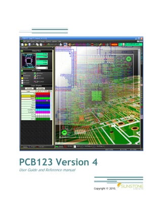
- 24. 23 Screen Layout More than one project at a time can be loaded into PCB123 and data can be copied between them. Each project loaded will appear as a tab at the top of the main window. Only one project can be active at any time and if more that one is loaded, the active project can be changed by clicking on its tab. Tabs from a 2-project session are shown left. Each project will have a minimum of four different views that can be displayed in the main window. They are Layout, 3D View, BOM (Bill Of Materials), and at least one schematic page. You can navigate between the views by clicking on the appropriate tab at the bottom of the main window. The strip of tabs is shown left. As you change views, different toolbars will come and go as different views are activated. To the left of the main window is the Edit Panel. It too contains a strip of tabs on the bottom as shown to the left. The Display tab is quite dynamic, changing its contents not only when the main window is switched between schematics and layout, but when certain types of objects are being edited context panes will be added and removed that provide various options for the selected object or tool. The Project tab contains several report generators and a top-level navigator in the form of a tree that allows you to drill down into the schematic and layout data in minute detail. It also contains many top-level settings and defaults such as title block parameters that can be set for a project. The DRC/ERC tab contains a live listing of all the current design violations in the project. As you can see, tabs are used extensively to display applicable tools and information and hide irrelevant tools and information for a given task.
- 25. 24 Common functionality Common functionality really refers to the common operations between the schematic view and the layout view. The 3D view and BOM view are highly specialized views that demand very little face time. By far, the design views will receive most of your attention so we will focus on the common functionality between them. A good deal of your time in the software will be spent moving the mouse around, poking the keyboard, and clicking on things. We hope we have created a fairly intuitive user interface but even so, we should cover some basic behavior. Pan and Zoom Because a PCB or a schematic can have a large number of objects packed into a small area it is next to impossible to do any work while viewing the entire extents of the data. Instead, you will want to be zoomed into and focused on a small area. Consequently, you will be doing a lot of panning and zooming. These operations are so common they become reflexive actions - you do not think about it, you just do it. First, under the View menu a Zoom submenu lists all the commands pertaining to zoom. The first four commands pertain to the view scale or zoom factor. Zoom In and Zoom Out magnify and… um… un-magnify the view. Using the menu commands or their keyboard accelerators, PgUp and PgDn, scale the zoom factor based on the ubiquitous Golden Ratio beloved since eternity. Using the mouse wheel scales the zoom factor by smaller increments. Zoom All adjusts the zoom factor and view center so the entire board outline fits within the viewport. The Zoom Actual Size command, which is not accelerated, relies on your display hardware to accurately report the number of pixels per inch of display and uses that factor to scale the view accordingly. The next four menu items pan, or scroll the view north, east, south, and west. The pan distance using these menu commands or their keyboard accelerators is the width or height of the window minus a comfortable overlap figure. Besides the obvious reasons for the overlap, it is interesting to note that panning by a full window can actually produce a “lost” sensation at times. The Redraw command will simply refresh the screen. It also rebuilds certain internal lookup tables and in rare situations, when you add or modify objects so their new extents are double or triple the size of the board you may find that you cannot pick them until a Redraw is performed or any number of other commands that trigger a regeneration of the tables is performed.
- 26. 25 Drilling into submenus is probably not the most efficient way to navigate around a design but Microsoft recommends standard practices and we try to oblige. The menu also shows the keyboard accelerators for the zoom commands. There is also a Zoom toolbar on the right edge of the application. It is lacking buttons for pan but there are stock scrollbars for that. The button labeled ‘G’ is not actually a zoom command at all. It is a way to invoke the Grid dialog using the mouse. As with most toolbars, you may hover your mouse over a button to pop up a tooltip for a brief description of the button’s operation. The Zoom Toolbar contains some of the lesser used commands such as Refresh Screen, Zoom All, and Zoom Actual Size. The Zoom Toolbar is for new users who don’t read the manual. You, however, deserve better. Most likely you will find that using the keyboard to perform zoom operations is superior to the menu and toolbar. The numeric keypad is dedicated to the zoom functions. The chart on the left shows the keypad assignments for the different zoom commands. By far, the best way to pan and zoom around the design canvas is to use the wheel on your mouse if it has one. The wheel can accomplish both pan and zoom. To zoom in, roll the wheel forward and to zoom out, roll it back toward you. The pan behavior is a byproduct of how Zoom In and Out work with the wheel. Wherever the mouse is pointing in the design window becomes the new viewport center. Zooming in and out actually does a pan so that whatever you were pointing at is now in the middle of the screen. The closer the mouse already is to the center, the finer the pan behavior. You point the cursor in the direction you want to pan and spin the wheel. It becomes very natural in just a short time. There is one additional behavior to mention. If you hold down the Shift key while moving the mouse in the main window then the window will smoothly pan in real-time. Names and Numbers Objects such as nets and components require unique names. Other objects may be optionally named or, in the case of PCB component pins, if they are named the names must be unique just within the component. In general, most objects that require a name will in fact have a name auto-generated during interactive design. Object names will be upper case and they currently will be restricted to the ANSI character set. There are no restrictions on name lengths. character set due to the stroked font requirements for Gerber data. In general, if you name an object do not include any spaces or other non-printable characters in the name. Whitespace, ‘|’, ‘&’, ‘[‘, and ‘]’ are reserved characters and will be replaced with an underscore ‘_’. Refresh Screen Pan Down Zoom Out Pan Left Pan Right Zoom All Pan Up Zoom In
- 27. 26 Unless absolutely necessary, names should not begin with numerical digits. There is nothing inherent in PCB123 for this, but names that begin with numbers may generate XML validation errors in 3rd party Plugins or future PCB123 facilities. The basic unit of measurement internal to PCB123 is 1/10,000,000th of an inch (one ten-millionth). This ensures that no conversion routines are required when switching between metric and imperial user units as the round off is insignificant. It does however mean that the extent of the world coordinate system is limited to +/- 200 inches as coordinates are stored as 32-bit integers. A 400-inch domain is more than sufficient for PCB boards and schematics but be careful if you intend to use the software for other purposes. When you supply values for physical parameters and coordinates, the values you enter are assumed to be in whatever the current system units are in. Additionally, four suffixes may be used when entering numeric data that allow an absolute unit basis to be specified. The table below lists these suffixes and shows examples of their use. Suffix Description Example in Inches 0.109in, -0.00002in mil Mils (1,000th of an inch) 109mil, -0.02mil cm Centimeters 0.27686cm, -0.0000508cm mm Millimeters 2.7686mm, 0.000508mm Anywhere the system asks for a physical value such as the Grid dialog box or a pad size form, you can perform local overrides of the current system units by supplying the appropriate suffix with the value. Any physical value can be entered as an expression so long as the terms are all in the same units. Expressions obey the C/C++ (normal) rules of operator precedence and associatively. Besides the arithmetic operators +, -, *, /, %(mod) the table to the left lists the functions that can be used in an expression. The ability to use expressions can come in real handy when creating footprints since most mechanical drawings of parts use relative dimensioning. The following table shows several examples for converting between polar coordinates and Cartesian coordinates. Objective problem What to type (in red) To locate an object at 15 degrees on a circle that is centered at 0,0 and has a radius of 2 inches. X = 2in*cos(15) Y = 2in*sin(15) Function Description abs(n) Absolute value of n acos(n) Arccosine (in degrees) of n asin(n) Arcsine (in degrees) of n atan(n) Arctangent (in degrees) of n sin(deg) sine of (degrees) deg cos(deg) cosine of (degrees) deg tan(deg) tangent of (degrees) deg log(n) Natural log of n log10(n) Base-10 log of n log2(n) Base-2 log of n sqrt(n) Square root of n
- 28. 27 To locate an object at 15 degrees on a circle that is centered at 4 inches,2 inches and has a radius of 2 inches. X=(2in*cos(15))+4.0 Y=(2in*sin(15))+2.0 Selection Important: PCB123 differs from many applications in how it treats a mouse click, where a click means pressing and releasing the left mouse button. In many popular applications, clicking on an object selects that object and waits for some operation to be performed on it. In PCB123 a click almost universally selects the object and immediately assumes a move operation on it – it is essentially tied to the cursor until another click releases it. If you hold down the Ctrl key when clicking on an object then it behaves like other applications and simply performs a select on it. In fact, multiple objects can be clicked and selected (or deselected) by holding down the Ctrl key while clicking objects. The way other applications accommodate an immediate move operation on an object is with a mouse drag, which involves pressing the left mouse button and moving the mouse while the button remains depressed. In most cases, PCB123 will accommodate that behavior too. The reason for the departure from standard click behavior is for sheer efficiency. A schematic document and especially a PCB document may contain many objects – tens of thousands in some cases. For this reason, any paradigm that shaves a click off an operation translates into a large cumulative gain in productivity. The details of the efficiency gains are covered under Object Editing later in this document. As you move the cursor over objects in the design windows you will notice they become temporarily highlighted. This is just a visual acknowledgement of which object will be selected if you were to click on it. If you let the cursor hover over an object you will get a tooltip displaying various properties of the object. The tooltip is translucent so as not to fully obscure objects beneath it. The image to the left shows a highlighted wire and its properties in a tooltip. Holding the Ctrl key down while clicking on objects performs a disjoined selection. A continuous selection can be performed by sweeping out a rectangular area which involves pressing the left mouse button down on a spot that contains no objects, dragging until the rectangle encompasses the objects you wish to select, and then releasing the left mouse button. Hold down the Ctrl key while doing so toggles the selection state of the objects.
- 29. 28 Objects are not automatically selectable. Objects that are set to invisible, either by object type or layer visibility will not highlight, nor are they selectable. Additionally, the Layout view has a toolbar, shown at right, which allows the selection of PCB object types to be toggled on or off. This can be very useful to prevent the accidental selection of some object types while performing certain tasks. For instance, while routing traces it can be a nuisance to miss picking a track by just a little and picking a component instead because it will begin moving the component off of any existing routes to the component pins. Of course you can always cancel the operation. Context Menus Pressing the Right Mouse Button (RMB) will always display a context menu populated with commands that are applicable to the current selection. If nothing was selected then an implied selection is carried out on the object the cursor was pointing to when the RMB occurred. Like the tooltip, the context menu (shown left) is translucent to prevent objects underneath the menu from being obscured. If several different types of objects are selected, the context menu may contain submenus for commands that operate on the different object types. Submenus are indicated by a right-pointing, right-justified arrow and will be displayed when the menu item is highlighted. In addition to the mouse, the arrow keys may be used to select different menu items. While a menu is active, all other activity in PCB123 is suspended until a menu selection is made or the menu cancelled. Commands PCB123 supports most of the common Windows editing commands such as Cut, Copy, and Paste. Currently, these commands are specialized to perform data interchange only between PCB123 documents. Undo and Redo is fully supported in PCB123 with one caveat: you cannot undo or redo a schematic edit while in Layout view, and vice versa. Undo and redo are unlimited as long as you remain in either view but as soon as you flip to the other view then undo and redo are flushed.
- 30. 29 Starting a New Design As previously mentioned, PCB123 attempts to accommodate a wide audience of which everyone, regardless of experience, needs to design a PCB. Your project may be using the most common off-the- shelf components and may need to fit in a standard housing but you still need to design that one custom part - the PCB. Because it is custom, the burden falls largely on you to ensure its correct design and operation. Good design software and good design practices will greatly aid you in this effort. PCB123 allows for the specification of rules that can ensure manufacturability and design continuity. Some of these rules can even be used to guarantee adherence to certain standards bodies’ rules such as the UL requirements for minimum spacing between nets of certain voltage potentials. There are issues associated with PCB design that can be extremely complex and are beyond the scope of this guide. As a rule of thumb, if you need to incorporate the electrical or temporal effects that the PCB has on nets as a function of the routing topology (transmission lines, crosstalk, emissions) then you may require more sophisticated (and very expensive) layout tools than PCB123 unless you are at an expert level in such matters. We do not have a button that ensures FCC compliance for your design but we do have a button that ensures everything is hooked up where it should be and nothing is shorted together. We also have a facility so you can add a button to ensure FCC compliance of a design by writing a Plugin that operates on the PCB data in any way you desire. PCB123 will automatically detect and report many of the problems that may arise during the design process. Even so, there are many places where the software cannot second-guess intent. How much checking the software will do, and even how much time the software can save you by performing some tasks automatically can be a direct result of how much information you supply PCB123 at the start of a design. First, let us look at the gross tasks involved in designing a board in PCB123. Overview of PCB design tasks Here is a quick list of the different tasks involved in designing a PCB. For now, it ignores how the design data is acquired and input into the system. It assumes you have already designed a schematic in PCB123 or input a netlist from another tool. This is covered in detail in the next section. The tasks are generally in chronological order but your design or your favorite techniques may differ slightly. The basic tasks are: • Using either the New Board Wizard or the Board Configuration Dialog, specify any manufacturing requirements for your design. These include the number of layers in the design, whether you desire soldermask and/or silkscreen on your boards, and certain non-standard requirements such as board thickness or copper weight. Some features are mutually exclusive and will be clearly indicated as such. All the configuration options can be changed at any time and are only finalized when ordering. However, some options can greatly impact the design rules which, if going from a less to a more restrictive set of rules, can be much more difficult to deal with in the later stages of a design. Examples of this would be specifying less layers than actually routed on, or changing from standard 1oz. copper to 2.5oz copper which requires greater spacing
- 31. 30 and feature sizes to properly etch the thicker copper clad. Incidentally, if you are new to this, then the concept of “adding layers” or “deleting layers” may be confusing to you. A PCB may have more than a front layer and a back layer. Two or more circuit boards can be independently etched and then carefully aligned and glued together, one on top of the other with an insulator between them. These boards are then drilled as one and the holes are then plated. The plated holes allow copper from one layer to be connected to copper on different layers. PCB123 handles 2, 4, and 6-layer boards as a standard process. For boards with more layers than that, you are requested to send the design to Sunstone for quick evaluation. You will then receive back the same design with the desired number of layers enabled and an adjusted price quote. • After the basic board configuration has been specified, ensure the size and shape of your board outline is correct. Closely associated with this is to correctly define and position any mounting holes or other hardware and to position any fixed electrical devices such as connectors, LEDs, and switches. In short, make sure the board will fit in a chassis or enclosure, that it can be secured in place if needed, and that any lights or dials that mount on the PCB are visible or accessible through openings in the enclosure. • Identify the electronic components that your design will use and either map them to “footprints” from our supplied libraries or create any custom footprints as needed. A footprint is a reusable stencil that defines the pattern of copper pads, drill holes, and silkscreen information such as the component outline and a reference designator (name) for the component. • Place all the components on the board so they don’t overlap or violate any special criteria that you may have such as height restrictions or proximity requirements such as locating filters near connectors or other sources. Once the critical mechanical and electrical requirements have been considered, the remaining components typically want to be placed in a way that minimizes the overall interconnect distance between components. Some components may require additional room around them to ensure there all the pins can be connected with routes. It is also desirable to place the components on as coarse a grid as possible. If all the pads are on a regular grid, then routing the board is much faster and easier because you will not have to make as many small bends around pads. • Distribute power and ground. Ensure the supply pins on semiconductors are properly decoupled by placing decoupling capacitors in close proximity to the supply pins. Bulk decoupling or filtering may want to happen close to the connector pins or devices supplying power to the entire board. If the board will have dedicated copper plane layers for power and ground then those nets should be assigned to the proper plane layers. If two or more nets are to share a plane layer but still be isolated from each other (called a split plane) then the isolation needs to be manually drawn on that plane layer. Surface mounted devices may need to have their power and ground pins routed out to a plated-through-hole that ties the surface pad to a plane layer. If the power and ground is to be distributed with routes and not plane layers, then they should be routed using traces that are wide enough to handle the required amount of power. Redundant routing in the form of a matrix may also be desired at the board extremities or at some regular interval to keep voltage levels uniform across all devices.
- 32. 31 • If any signal nets have critical requirements such as complimentary routing or matched/critical length, or they require special attention such as pin-to-pin route sequencing, then these nets should be routed before other nets. • Route all the remaining interconnections. This can be the most time consuming task in PCB design and there are many strategies that can be used. One strategy that is almost always a winner is to assign a direction to a routing layer. There can be a lot of flexibility in this, but by routing mostly vertical on one layer, and horizontal on a different layer, you will be much less likely to create blockages for layer routing. The layers will have a “flow” to them and changing between layers by using vias as the routing direction changes can typically utilize the layers much more efficiently. If your design is moderately to very dense, and a sizable percentage of it uses surface mounted devices, then you can expect that the surface layer(s) will be consumed by short routes that escape a surface pin to a via (a plated drill hole) to effectively allow that pin to be routed on any layer. This process is known as Fanout routing and should be done before bulk routing. It is not only a time saver for bulk routing but can be an early indicator of problems. If you cannot fanout a device then you most likely will not be able to completely route that device without making more room around it, adjusting its location, or adding more routing layers. It is much better to discover these kinds of problems earlier than later. Moving a component after it has been routed hurts more than moving it before it was routed. Additionally, you may have struggled to route most of a dense design only to find that you need two more routing layers to complete the rest of it. Knowing this up front would have made the routing easier right from the beginning. • When all routing is finished, you may wish to improve power and ground distribution or provide ground shielding by flooding regions of the board with a copper plane that is tied to a power or ground net. Any object in the region that does not belong to a net, or has a net other than that of the copper region will be automatically isolated from the copper region. These regions are collectively known as copper pour. • The next task will be to perform a Design Rule Check (DRC) and address any problems that it may have uncovered. The DRC will report on shorts, opens, and violations of manufacturing rules such as minimum spacing between objects of different nets, and pad size vs. drill size violations. Some reported violations such as problems with the silkscreen can be ignored at this stage but certainly DRC violations on routing layers and plane layers should be addressed at this stage. • If your board is to have silkscreen on it, then you will want to place the component reference designators so they can be seen after the board is populated with components. This usually involves moving the reference designators outside the component outlines but close enough to the correct component to prevent an ambiguous reading of which name belongs to which component. You may also wish to add other nomenclature to your design such as the name of the board, a company logo, jumper configurations, or other wording or drawings. Nomenclature can be added to copper layers and silkscreen layers. If text is added to the bottom routing layer or bottom silkscreen then that text should be “mirrored” so it will read correctly when the finished board is flipped over in your hand to observe the back. After adding your nomenclature, you will want to run an additional DRC to make sure you didn’t short anything together or create silkscreen on any pads.
- 33. 32 • As a final check, you may wish to view your design in 3-D. PCB123’s photorealistic 3-D viewer may allow you to visually spot problems that DRC assumes are correct. Because it displays the board in perspective and from any viewing angle, certain errors such as wrong/missing drill sizes or unreadable silkscreen text tend to really stand out compared to looking only at the orthogonal 2-D view. Once you are satisfied that it looks correct and DRC is reporting no errors then you can press the Order button which guides you through the order process. Depending on the board complexity and the time of day you placed the order, you will receive your boards anywhere from 2-5 business days later. Data Requirements PCB123 provides a host of tools to complete all the different tasks but many of them are highly dependent on how you specify or acquire the design data. This can be broken into two methods: with a schematic, or without a schematic. To be even more specific, your design has been “captured” inside a schematic program, or your design resides on a napkin, in a picture, or in your head. It takes effort to capture a design with schematic software but this effort usually pays great dividends. Unless your design is extremely simple and involves only a few parts, it is strongly recommended that you create an electronic schematic of the design before attempting layout. PCB123 provides a schematic capture facility that works in lock-step with its layout facility. In addition, PCB123 also is capable of reading and importing netlists that have been generated by other schematic capture programs. In case you are unfamiliar, a netlist is a file that lists all the components used in a design and defines how those components are connected together. A component, or part, is usually specified in a netlist as a name/type pair. A component name, or reference designator, typically consists of an alpha prefix and a numerical suffix such as R1 or U15. Reference designators must be unique in a design. The component type, or part type, might appear as anything from a proprietary description such as RES_33-OHM_1/4W to a manufacturer’s part number such as SN74LS00N. In some cases, the component may also be augmented with additional data such as the name of a standard package or footprint for the part. After all, a 33-ohm, ¼ watt resistor can come in many physical sizes and shapes. The connectivity information in a netlist is usually specified at the “net” level. A net has a name such as +5V, GND, or RESET, and has a list of one or more “nodes” or pins in the form of R1.2, which reads “pin 2 of component R1.” A net with one node is legal but unusual. The vast majority of nets consist of two or more nodes. A net with two or more nodes inside PCB123 will be displayed as pin-to-pin wires that must be connected by a continuous copper path or plane. Until PCB123 V3, a netlist was the traditional data transport from a schematic program to a layout program. For the first time, PCB123 eliminates the netlist as a data transport as long as the schematic was designed in, or converted to a PCB123 schematic. A schematic designed in PCB123 has a more intimate relationship with the layout than does a netlist from another program. Using a netlist from a different schematic program has the following disadvantages: • A netlist is a static snapshot of a schematic at a particular moment in time. If changes are made to the schematic then a new netlist must be generated that reflects the changes. If the PCB layout is already in progress, then the PCB must be synchronized with the new netlist. Luckily
- 34. 33 there are facilities for this but if the schematic was created in PCB123 to begin with, any change to it is instantly reflected in the layout and vice-versa. • A netlist is not certain to contain part references that are known to PCB123. These unknown references must be resolved. This can actually be done interactively while reading the netlist because whenever an unknown part type is encountered, you will be presented with a browser that allows you to find and graphically verify a footprint from a library to use for the part type. A native PCB123 schematic, on the other hand, will not even allow a schematic symbol to be placed on a page unless it has already defined the PCB footprint it uses, and verifies that the footprint can be found in the library. • Very little context from the schematic is retained in a netlist. That a net is connected to a power or ground symbol is not reflected in the netlist. If it were, than that net could automatically be made to use fatter routing widths. A PCB123 schematic automatically uses that kind of contextual information to adjust the layout rules as needed. A netlist is also missing proximity information or any data that indicates how the schematic was organized by page or through a hierarchy. This information is expected to be widely used in future releases of PCB123 for such things a grouping, replication, and as hints to the autoplacer. • Changes initiated from the PCB design, such as adding a decoupling capacitor, must be manually performed over in the other schematic program. If this is not done then there will be a mismatch when comparing the two databases and performing another netlist comparison will run the risk of undoing the changes, in this case deleting the newly added decoupling capacitor. As mentioned before, PCB123 always synchronizes changes from either side to the other. There is nothing to remember or relay to someone else. Despite the disadvantages listed above, using a netlist from another system is far superior than designing a PCB without one. Most schematic programs have some facility for performing an Electrical Rules Check. This can flush out logic errors very early by detecting such things as outputs connected to outputs or anything connected to a pin designated as N/C (not connected). Many schematic programs also host simulators that can verify the correct operation and timing of circuits. Additionally, capturing your design in a PCB123 schematic or in a netlist allows automated tools in layout such as the autoplacer and autorouter to be used. These tools can save hours or days of labor or they can also be used for early decision-making and early identification of problems. Though PCB123 allows you to create your PCB design using piecewise primitives such as individual pads and line segments, it is not recommended except in the most trivial designs. These designs miss the benefits of context checking and many powerful automatic tools.
- 35. 34 The New-Board Wizard When you first run PCB123, you will first see either a “Latest Information” window or a “Checking for Updates” window, both that assume a connection to the internet. If the computer is not connected to the internet, then a message indicating that fact is displayed. The “Latest Information” window is a small web page that is periodically updated to reflect new services, promotions or important notices. Every so often, the software checks if a new version is available for download. If a new version is available, a summary of new features and bug fixes is presented along with the option of downloading and installing the new version. If you continue to run with older software, you will be asked to update about every tenth time you run the software. You can always check for, and install new updates yourself from the PCB123 menu. After dismissing the “Latest Information” or “Checking for Updates” window, you will be presented with the first step of the “New Board Wizard”. If you want to load an existing design or just start fiddling with the software, you can click the Cancel button or press the Esc key to dismiss the wizard. The New Board Wizard is primarily for new users but many find it useful to begin a new design no matter how long they have used the system. The Wizard has been carried forward from version 2 to version 3 virtually untouched, which makes it a highly board-centric feature. It never even mentions the word ‘Schematic’ once and PCB123 reserves the right to change the Wizard in the future to make it more Project-centric as other Project-level behavior is defined or requested. The New Board Wizard has 4 pages of which the first one is shown below: The Board Name field is essentially the title of your new design and can be anything as long as it is not empty. The Netlist File field is optional. If you have captured your design in a schematic program other than PCB123, then you can either type the name of the netlist file or, more likely, click on the Browse.. button to invoke a standard Windows file dialog box that allows you to navigate to the file. If you do click the browse button, the ‘Files of Type’ will list all the netlist formats currently recognized by PCB123. The netlist will not be read until the wizard is finished.
- 36. 35 Clicking on the Next button brings you to step 2 as shown below: You have a choice of defining your board size by entering a rectangular width and height for your board or selecting an existing board template supplied by Sunstone, a third party, or created previously by you. When selecting templates, you will get a postage-stamp preview of the template. Templates most likely will contain a board outline but may also contain tooling holes, dimension lines, title blocks, and even components such as connectors. Because a netlist may define a component and a template may define a component there exists the possibility for a conflict. If they both attempt to load in a component with the same name, then the component in the template wins and will be used in place of the one in the netlist. A warning will be issued to that effect. The template component wins because it contains a more complete specification by including location, rotation, and board-side data. Step three is where you specify the number of layers in your design and how those layers are used. It appears below:
- 37. 36 In the Number of Layers section, you can select two, four, or six layers for your design. The default is two layers. Selecting more than two layers will enable the Inner Layer Type options. You may need more than two layers because of a mechanical requirements such as high component and interconnect density and unfavorable interconnect topology, or for electrical reasons such as cleaner power distribution and transient return paths, or to form transmission lines on critical nets. You will have to specify which nets are assigned to the plane layers. Any pin belonging to the specified nets will tie to the plane at a plated hole. This plane connection does not occur against a solid plane, but instead the plated hole has an isolation gap around it with “spokes” that bridge the gap at certain places. This isolation prevents the plane layer from sinking too much heat during soldering. It focuses the heat on the pin and allows for a clean solder bond.