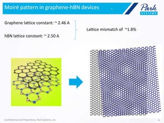
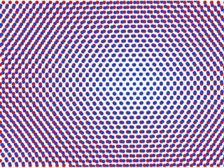
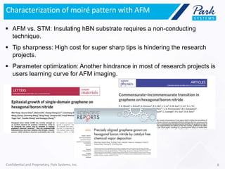
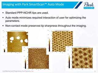
www.parkafm.com
Imaging Moiré Pattern using
SmartScan™ Auto Mode
Park Systems, Inc.
2015
Confidential and Proprietary, Park Systems, Inc.
What is a Moiré pattern?
Confidential and Proprietary, Park Systems, Inc. 2
Potential Applications of graphene
Higher mobility needs appropriate substrate… .
Confidential and Proprietary, Park Systems, Inc. 4
Production methods of Graphene/hBN devices .
- Low yield
- Random
Orientation of
graphene
- Unreliability in
electrical
properties
Direct transfer
- Essentially same
as graphene
growth method
- Complexity in
transfer process
Metal catalytic
CVD
- Graphene growth
on hexagonal BN
- Graphene
nucleation at
substrates defects
CVD without
metal catalyst
Graphene lattice constant: ~ 2.46 A
Lattice mismatch of ~1.8%
hBN lattice constant: ~ 2.50 A
Moiré pattern in graphene-hBN devices .
Confidential and Proprietary, Park Systems, Inc. 6
Moiré pattern in graphene-hBN devices .
Confidential and Proprietary, Park Systems, Inc. 7
Characterization of moiré pattern with AFM
Confidential and Proprietary, Park Systems, Inc. 8
 AFM vs. STM: Insulating hBN substrate requires a non-conducting
technique.
 Tip sharpness: High cost for super sharp tips is hindering the research
projects.
 Parameter optimization: Another hindrance in most of research projects is
users learning curve for AFM imaging.
Imaging with Park SmartScan™ Auto Mode
 Standard PPP-NCHR tips are used.
 Auto mode minimizes required interaction of user for optimizing the
parameters.
 Non-contact mode preserves tip sharpness throughout the imaging.
Confidential and Proprietary, Park Systems, Inc. 9
Park Systems
is a leading manufacturer of atomic force microscopy (AFM) systems
with a complete range of products for researchers and industry
engineers in materials science, chemistry, physics, life sciences,
semiconductor and data storage industries. Park’s products are used by
over a thousand of institutions worldwide. Park’s AFM features unique
patented set of technologies that yields highest data accuracy at
nanoscale resolution, superior productivity and ease of use, and lowest
operating cost to its customers. Park Systems, Inc. is headquartered in
Santa Clara, California with its global manufacturing, and R&D
headquarters in Korea. Park’s products are sold and supported
worldwide with regional headquarters in the US, Korea, Japan, and
Singapore, and distribution partners throughout Europe, Asia, and
America.
Please visit www.parkafm.com or call 408-986-1110 for more
information.
ABOUT US
Confidential and Proprietary, Park Systems, Inc. 10
Thank you.
For more information, please contact:
Park Systems, Inc.
T: 408-986-1110
E: ardavan@parkafm.com
Confidential and Proprietary, Park Systems, Inc. 11

Park Systems Graphene moire

  • 1.
    www.parkafm.com Imaging Moiré Patternusing SmartScan™ Auto Mode Park Systems, Inc. 2015 Confidential and Proprietary, Park Systems, Inc.
  • 2.
    What is aMoiré pattern? Confidential and Proprietary, Park Systems, Inc. 2
  • 3.
  • 4.
    Higher mobility needsappropriate substrate… . Confidential and Proprietary, Park Systems, Inc. 4
  • 5.
    Production methods ofGraphene/hBN devices . - Low yield - Random Orientation of graphene - Unreliability in electrical properties Direct transfer - Essentially same as graphene growth method - Complexity in transfer process Metal catalytic CVD - Graphene growth on hexagonal BN - Graphene nucleation at substrates defects CVD without metal catalyst
  • 6.
    Graphene lattice constant:~ 2.46 A Lattice mismatch of ~1.8% hBN lattice constant: ~ 2.50 A Moiré pattern in graphene-hBN devices . Confidential and Proprietary, Park Systems, Inc. 6
  • 7.
    Moiré pattern ingraphene-hBN devices . Confidential and Proprietary, Park Systems, Inc. 7
  • 8.
    Characterization of moirépattern with AFM Confidential and Proprietary, Park Systems, Inc. 8  AFM vs. STM: Insulating hBN substrate requires a non-conducting technique.  Tip sharpness: High cost for super sharp tips is hindering the research projects.  Parameter optimization: Another hindrance in most of research projects is users learning curve for AFM imaging.
  • 9.
    Imaging with ParkSmartScan™ Auto Mode  Standard PPP-NCHR tips are used.  Auto mode minimizes required interaction of user for optimizing the parameters.  Non-contact mode preserves tip sharpness throughout the imaging. Confidential and Proprietary, Park Systems, Inc. 9
  • 10.
    Park Systems is aleading manufacturer of atomic force microscopy (AFM) systems with a complete range of products for researchers and industry engineers in materials science, chemistry, physics, life sciences, semiconductor and data storage industries. Park’s products are used by over a thousand of institutions worldwide. Park’s AFM features unique patented set of technologies that yields highest data accuracy at nanoscale resolution, superior productivity and ease of use, and lowest operating cost to its customers. Park Systems, Inc. is headquartered in Santa Clara, California with its global manufacturing, and R&D headquarters in Korea. Park’s products are sold and supported worldwide with regional headquarters in the US, Korea, Japan, and Singapore, and distribution partners throughout Europe, Asia, and America. Please visit www.parkafm.com or call 408-986-1110 for more information. ABOUT US Confidential and Proprietary, Park Systems, Inc. 10
  • 11.
    Thank you. For moreinformation, please contact: Park Systems, Inc. T: 408-986-1110 E: ardavan@parkafm.com Confidential and Proprietary, Park Systems, Inc. 11

Editor's Notes

  • #3 It's caused by the interference pattern between the pixel grid in your camera's sensor, the pixel grid on the screen your photographing and the pixel grid on your phone's screen (which is why they change when you zoom) If you take a picture of window screen or other regular square pattern you can see the same thing. You can even see them in the real world by looking through two layers of wire screens (an appropriate distance apart) (The reason they're curved is because different parts of the monitor are different distances from the camera sensor so the interference frequency changes .)