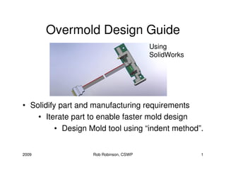
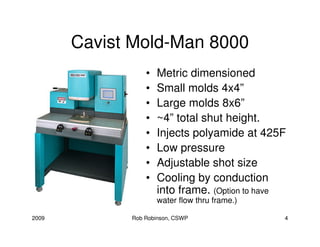
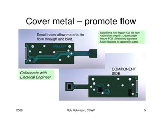
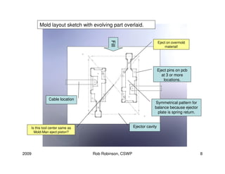
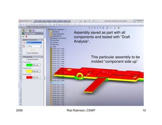
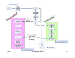
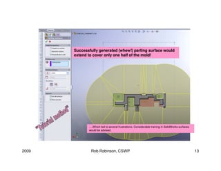
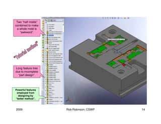
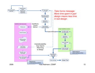
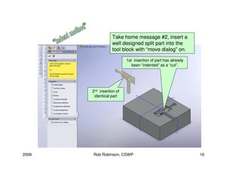
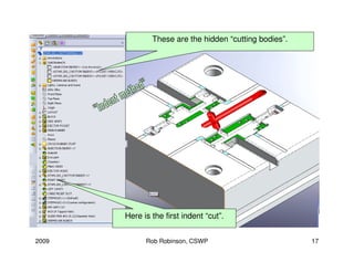
Vacuum technology products used in food, packaging, pharmaceutical, automotive and any application requiring pick and place or handling material. Samples of End of arm tooling technology for robots EOAT.
This document discusses resistive sensors and their applications. It begins by defining resistive sensors as transducers that convert mechanical changes into electrical signals by changing resistance. Common resistive sensors include potentiometers, strain gauges, thermocouples, photoresistors and thermistors. The document then covers the theory of how resistance changes based on length, area, composition and temperature. It provides examples of specific resistive sensors and their typical applications, such as using light dependent resistors for light switches and strain gauges for sensors in electronic balances. In closing, it discusses how the resistance of sensors varies with changes in factors like temperature, strain or light intensity.
This document discusses thermistors, which are temperature sensing elements that measure temperature through changes in resistance. It describes how thermistors are constructed from sintered semiconductor materials and come in various shapes. The document outlines the working principle of thermistors, types including positive and negative temperature coefficient thermistors, advantages like low cost and high sensitivity, disadvantages such as non-linear output, and applications including current limiting devices, digital thermostats, and battery pack monitors.
Faculty of Engineering & Technology , Gurukula Kangri University , Haridwarashwini kumar
Topic:- Tachometer
Description :- This is use to measure the speed of rotating machines in rpm....
Ashwini kumar
Electrical Engineering
ashwinikmr555@gmail.com
+919027134556
This is a presentation that I put together that explains the basic manufacturing process for printed circuit boards. There are many different ways to build a board. This presentation explains the basics of the most common operations. This is a general overview. For more information on the subject visit www.pcbdesignschool.com
A piezoelectric sensor uses the piezoelectric effect to convert changes in pressure, acceleration, temperature, strain or force into an electrical charge. Piezoelectric sensors are versatile tools that are used for quality assurance, process control, and research and development across many industries. They have limitations for static measurements but are otherwise a mature and reliable sensing technology. Piezoresistive sensors undergo a change in electrical resistance when subjected to mechanical strain, and are commonly used in integrated circuits made from piezoresistive materials like silicon.
Ceramics are inorganic, non-metallic materials that are brittle but strong in compression. There are several types of 3D printers that can print with ceramics, including modified FDM printers that extrude clay-like filament or paste, the WASP printer which has an add-on ceramic extruder, and the PotterBot which is exclusively for ceramics. New SLA techniques are also enabling ceramic 3D printing.
In this presentation, we cover how to pick the right technology to measure a coating thickness.
- An introduction to coatings
- Why coatings are used in industry
- Why to measure the thickness of a coating
- The best methods for coating thickness measurement
For more information, visit: Olympus-IMS.com.
A calender is a machine that processes polymer melts into sheets or films using heat and pressure between rollers. It works by softening the polymer and passing it through nips between two or more rollers to form a continuous sheet, with the thickness determined by the gap between the last rollers. Common uses of calendered sheets include flooring, rainwear, wall coverings, and signage. Thermoplastics are well-suited for calendering as they can soften without fully melting. Different roller configurations like I, L, and Z types address issues like separating forces between rollers. Calendering is advantageous for heat-sensitive materials but high capital costs and achieving precise thickness can be challenges
The document discusses Fast Fourier Transform (FFT) analysis. It begins by explaining what Fourier Transform and Discrete Fourier Transform (DFT) are and how they convert signals from the time domain to the frequency domain. It then states that FFT is an efficient algorithm for performing DFT, allowing it to be done much faster on computers. The document proceeds to describe different types of FFT algorithms like Cooley-Tukey, Prime Factor, Bruun's, and Rader's algorithms. It concludes by discussing characteristics of FFT like approximation, accuracy, and complexity bounds, as well as applications and how FFT can be used to analyze vibration signals in the frequency domain.
This document discusses various polymer processing techniques. It begins by outlining three general phases of plastics processes: heating, shaping/forming under constraint, and cooling. It then describes specific processes like thermoforming, compression and transfer molding, rotational molding, extrusion and extrusion-based processes, injection molding, and blow molding. For each process, it provides details on how it works, its advantages and disadvantages, and common applications.
This document provides an introduction to vibration measurement, including:
- Why vibration is measured, where it comes from, and what vibration is
- How to quantify vibration levels using parameters like acceleration, velocity, and displacement
- Details on piezoelectric accelerometers, which are commonly used to measure vibration
- Factors to consider when taking vibration measurements, like sensor mounting, environmental influences, and instrumentation
1. The document discusses various types of sensors including electromagnetic sensors, mechanical sensors, and gas sensors. It provides details on common sensors like resistance sensors, current sensors, voltage sensors, and pressure sensors.
2. Examples of applications mentioned include uses in automobiles, industry, medicine, aerospace, process control, environmental monitoring, and more.
3. The operating principles of different sensors are explained, such as how resistance sensors measure resistance, current sensors detect current, and pressure sensors convert pressure into electrical signals.
The document discusses several common sensor types used for vibration measurements, including accelerometers, velocity sensors, proximity probes, and laser displacement sensors. Accelerometers use piezoelectric crystals to generate a charge proportional to acceleration. Velocity sensors induce a voltage in a coil moving through a magnetic field, proportional to velocity. Proximity probes measure displacement using capacitive or eddy current techniques. Laser displacement sensors use triangulation to determine position with high accuracy. Each sensor type has advantages and disadvantages for different vibration measurement applications.
The document discusses vibration dampers and damping. It defines damping as the ability of a vibrating system to dissipate energy, often by converting mechanical energy to heat. There are two main types of damping: material damping from a material's internal friction, and structural damping from friction between assembled parts. Measurement of damping involves analyzing hysteresis loops for materials or conducting vibration tests on structures. Common damping techniques include using viscoelastic dampers, dynamic dampers, and controlling resonance peaks through damping.
The document discusses various fiber reinforced plastic (FRP) composite manufacturing processes. It defines FRP composites and describes common matrix materials like thermoset and thermoplastic resins. Manufacturing methods covered include hand lay-up, spray-up, resin transfer molding (RTM), filament winding, pultrusion, matched-die molding, and reaction injection molding (RIM). Each process is explained along with associated materials, equipment, advantages, disadvantages and applications.
The document discusses the static and dynamic performance characteristics of measuring instruments. It describes how instruments can be modeled as zero-order, first-order, or second-order systems depending on how their output responds to changes in input over time. Zero-order instruments have an immediate output response, while first-order instruments exhibit a lag due to a time constant. Second-order instruments may also oscillate before reaching steady-state. Examples are given like thermometers and potentiometers to illustrate different order responses. Dynamic inputs like step, ramp and periodic signals are also discussed to analyze instrument behavior under transient and steady-state conditions.
The document provides an overview of injection moulding, including:
- The history of injection moulding beginning in the 1870s.
- The injection moulding process which involves injecting molten plastic into a closed mould.
- The main types of injection moulding machines: hand, plunger, and reciprocating screw types.
- Key machine components like the screw and their functions in plasticizing and injecting the material.
- Common materials used for injection moulding like ABS, nylon, polypropylene.
Data acquisition involves sampling signals from physical processes, converting the analog signals to digital numeric values, and processing the data with a computer. Data acquisition systems typically use transducers to sense physical variables and convert them to electrical signals, condition the signals for analog to digital conversion, and convert the signals to digital formats for computer processing, analysis, storage and display. Signal conditioning improves signal quality and may include amplification, isolation, filtering and linearization. Analog to digital converters change analog voltage or current levels into digital values that computers can process.
This document provides information about the AE-681 Composite Materials course taught by Dr. PM Mohite. The course covers topics such as introduction to unidirectional composites, analysis of lamina using classical laminate theory, design considerations, micromechanics, and performance under adverse environments. Reference materials include textbooks on composite materials and research papers. Students will be evaluated based on midterm exams, assignments, and a final exam. Attendance will be monitored and late or copied assignments will be penalized.
The document discusses a technical seminar on BiCMOS technology. It begins with an introduction and describes the characteristics and fabrication processes of CMOS, bipolar, and BiCMOS technologies. BiCMOS combines the advantages of CMOS, like low power and high density, with bipolar's high speed and current drive. While more complex than CMOS, BiCMOS provides improved performance over both CMOS and bipolar. The document outlines the advantages and applications of BiCMOS, such as mixed-signal integrated circuits, and compares it to CMOS and bipolar technologies. It concludes with a literature survey on books and websites relating to BiCMOS design.
An accelerometer is a device that measures acceleration forces. It contains capacitive plates that move relative to each other in response to acceleration, changing capacitance. This capacitance change can be converted to a voltage proportional to acceleration. Accelerometers are used to measure vibration in many fields. They are specified by factors like range, sensitivity, bandwidth, and axes. Common types include capacitive, piezoelectric, and strain gauge accelerometers. Proper calibration ensures the electrical output accurately represents measured acceleration.
LED, BGA, and QFN Inspection - X-Ray Inspection for SMT Quality Assurance and...Bill Cardoso
In this presentation we will cover the manufacturing of the most challenging surface mount parts to assemble and inspect today: LEDs, BGAs, and QFNs. The presentation will focus on the pitfalls of manufacturing and inspecting PCBs with these devices and solution to the technical challenges encountered by luminaire integrators and contract manufacturers. This presentation is targeted at manufacturing, process, and quality personnel responsible for designing; implementing and/or controlling the surface mount device application and inspection process. Those personnel responsible for training operators and technicians to perform assembly inspection or control the manufacturing process would also benefit from this presentation.
This document describes a new type of battery that is safer and longer-lasting than current lithium-ion batteries. It works by using sodium ions rather than lithium ions to store and release energy. Sodium is more abundant than lithium, which could make the batteries more affordable to produce. The new batteries maintain most of the energy density of lithium-ion batteries and can charge and discharge thousands of times before showing degradation. They represent a promising alternative battery technology.
The surface finish forms a critical interface between electronic components and printed circuit boards. It protects exposed copper circuitry and provides a solderable surface for assembling components. Common surface finishes include HASL, lead free HASL, immersion tin, immersion silver, OSP, and immersion gold, with factors like cost, reliability, and environmental compliance influencing the choice of finish.
There are three main types of flexible circuits: static, flex-to-install, and dynamic. Static circuits are not meant to flex, flex-to-install circuits are meant to flex only during installation/repair and can withstand limited flexing, and dynamic circuits are designed to withstand repeated flexing of over 1 million cycles. Key considerations in flex circuit design include avoiding stacked traces, using hold-down tabs, and calculating minimum bend radii based on circuit thickness. Common flex circuit materials include polyimide films like Kapton but PCB Solutions recommends Taiflex for most applications.
Rule Properties dialog will appear. Here you can:
This document provides a comprehensive reference on setting up - Edit the rule name
design rules for PCB design in Altium Designer. It covers defining - Select the scope of the rule
rules for electrical, placement, routing, manufacturing, and other - Edit the constraint attributes like clearance values
categories. Rules ensure design requirements are followed and can - Set the rule's priority
be checked during design. The software allows exporting and - Enable/disable the rule
importing rule sets for different projects. - View rule dependencies
The document discusses advanced ceramic substrates for microelectronic systems. It describes desired substrate properties such as high electrical resistivity and thermal conductivity. It also discusses common ceramic materials used as substrates like silicon carbide and aluminum nitride and their fabrication methods. The document outlines the definitions, thermal, mechanical, and electrical properties to consider for ceramic substrates. It also covers metallization techniques for ceramic substrates, such as thick film and thin film processes.
Rapid prototyping technologies,applications &part deposition planning 2Johnbin Johnson
Rapid prototyping technologies allow for the quick fabrication of scale models using 3D CAD data. The document discusses several rapid prototyping processes like stereolithography, fused deposition modeling, and selective laser sintering. It also covers part deposition planning, which determines part accuracy, surface quality, build time and cost based on factors like tessellation, slicing, and orientation. While rapid prototyping enables faster design iterations, limitations include poor surface finish and limited strength compared to final production parts.
This document discusses selective laser melting (SLM) technology for manufacturing conformal cooling inserts for injection molds. It describes how SLM allows for complex internal channel geometries to optimize cooling. Several case studies show how SLM inserts improved temperature uniformity, reduced cycle times, and eliminated part warping compared to traditional drilled inserts. Mold designers can leverage SLM to integrate optimized cooling at the design phase for maximum benefits.
Ironwood Electronics offers high performance test sockets and adapters for both laboratory and production use. IC packages covered include QFN, BGA, SOIC, QFP, and other SMT packages.
This presentation is by John Coonrod from the Advanced Circuit Materials Division at Rogers Corporation. It addresses how to determine the dielectric constant (Dk) in circuit materials for printed circuit boards and electronics.
Improving Manufacturing by Simulation: Processes, Microstructure & ToolingWilde Analysis Ltd.
This presentation, made at the inaugural Virtual Engineering Centre Workshop on 25-26th October 2011, provides an overview of the application of simulation to optimise manufacturing processes and determine mechanical properties that can affect in-service performance. These properties can be imported into structural FEA programs such as ANSYS for subsequent analysis of the final product.
Wilde Analysis believes that simulation techniques can play an important part in ensuring that parts are produced to a required standard and in an efficient way. Many of us are aware of simulation techniques such as finite element analysis (FEA) and computational fluid dynamics (CFD) being applied to product design.
These techniques are now used extensively in product development for applications such as checks on structural integrity or pressure drops in fluid applications. However, fewer people are aware of the application of these and similar techniques to design and optimise the manufacturing processes and how they can deliver benefits in areas such as metal forging, machining, heat treatment and the injection moulding.
The simulation of any one of these processes is technically demanding, but is now used extensively by many manufacturers, some of whom will not commit to making tools to produce a new part without first ‘proving’ the process using simulation. These simulations require advanced techniques including the modelling of non linear materials, large displacements, evolving contact surfaces and material removal in a multi-physics environment.
Having mastered the modelling of a single process, the technology is now being applied to multi-stage modelling to simulate multiple operations and predict final properties that can affect in-service performance. This presents many new challenges and for some applications it’s still at the research stage. Nevertheless, current technologies are now being used to optimise manufacturing processes.
JSK Innovative Technology Pvt Ltd is an ISO certified electronics company that specializes in home automation products like LED drivers. It discusses the PCB design and manufacturing process, including types of PCB boards, materials used, design software, manufacturing steps, and surface mount vs through-hole assembly techniques. The document provides details on each stage of the PCB design and production process.
Drilling Bit Introduction and bit Selection (Part 3)Amir Rafati
(PART 1,2 & 3)
1. Drilling mechanisms
2. Bit classifications (fixed cutter and roller cone bits)
3. IADC code descriptions
4. Tri-cone bits life time
5. Geometrical analysis of roller cone bits
• Fundamentals of bit design
• Basics of cone geometry design
• Oversize angle
• Offset
• Teeth and inserts
• Additional design criteria: tooth to tooth and groove clearances and etc.
• Cone-shell thickness
• Bearings factors
• Rock bit metallurgy
• Heat treatment
• Legs and cones material
• Tungsten carbide materials
• Legs and cones hard facing
• Tungsten carbide grade selection for inserts
• Bearings, seals and lubrication
• Bearing shape
• Bearing precisions and geometry
• Seal systems and seal details
• Dull grading system
6. Geometrical analysis of PDC bits
• PDC materials and constructions
• Matrix materials testing
• Differs between matrix & steel body
• Matrix body bits manufacturing
• Steel body bits manufacturing
• PDC bit design parameters: mechanical, hydraulic, rock properties
• Weld strength of PDC bits and cutters
• PDC cutter manufacturing process
• Tsp cutter properties vs PDC
• The influences of bit profile and profile elements
• PDC forces
• PDC bit stability
• PDC bit steer-ability
• Back rake
• Side rake
• Depth of cut
• Cutter exposure
• Cutter density
• Thermal damage and degradation of cutters
• Cutting mechanics
• PDC cutter substrate and its thickness
• Cutting structure elements
• Single set bladed cutting structures
• Plural set bladed cutting structures
• Dull grading system
7. ROP management based on drilling parameters
• WOB
• Rpm
• Sold content of mud
• Mud weight
• Cutter shape
• Cutters geometry
• Depth
• Abnormal pressure
• Drilling formation properties
The document discusses interconnection techniques for integrated circuits, including Tape Automated Bonding (TAB) and flip chip. TAB involves mounting an IC die on a flexible polymer tape with copper beam leads bonded from the die pads to the tape. There are different TAB tape structures. Flip chip involves mounting an IC die face down onto a substrate or circuit board using solder bumps on the die pads. Key aspects of flip chip covered include the interconnect system components, advantages like higher density and performance, and disadvantages like needing more processing steps. Under bump metallization is described as a multilayer thin film deposited on die pads to protect from corrosion and improve solder wetting.
The NM200UW nuclear underwater laser scanner is a landmark technology developed by Newton Labs in partnership with a major U.S. nuclear utility.
The NM200UW system combines rugged, industrial-grade hardware and electronics with sophisticated, Newton-developed software that compensates for the disruption of turbulence, heat and radioactivity characteristic of the in-vessel environment.
The scanner output is a point cloud so detailed, that when utilized with industry standard, three-dimensional software, a fully measurable CAD model can be generated.
The capability of the NM200UW to provide precise, reliable and efficient dimensioning of as-built features, as well as to track cycle-to-cycle degradation, is important to nuclear utility operators, who until now have relied heavily on indirect, inexact measurement techniques.
Designing For Flexibility And ReliabilityAbdul Khan
This document discusses factors that contribute to the reliability of flexible printed circuits (FPCs) that experience flexing during use. It covers the benefits of FPCs including reduced weight and space, improved packaging, and increased functionality. The document discusses standard FPC constructions, materials, manufacturing capabilities, design guidelines, and considerations for designing FPCs to function reliably under flexing conditions.
The Shift to 3D-IC Structures - Manufacturing and Process Control Challengeschiportal
The document discusses the manufacturing and process control challenges of 3D integrated circuit structures. It describes how 3D architectures are being implemented in vertical NAND flash memory and FinFET transistors. The key challenges for 3D manufacturing include precise control of thin film deposition, etch profiles, and detection of defects embedded deep within complex multi-layer stacks. Semiconductor metrology and inspection tools will need to advance to allow 3D imaging and measurement of features located in the third dimension.
The document discusses the shift to 3D integrated circuit structures and the manufacturing and process control challenges involved. It describes how 3D NAND flash memory uses a vertically stacked structure to increase density in a cost-effective manner. Implementing FinFET transistors also builds vertically by using fin-shaped gates on three sides to improve performance. Significant challenges include precise control over multiple thin film depositions and complex etch processes needed for these 3D structures. Advanced metrology and inspection is required to monitor critical dimensions, material properties, defects and other parameters in three dimensions.
The document provides tips for doing well in VLSI design such as attending classes regularly, working independently on assignments, studying effectively in groups, asking questions, and not cheating on exams. It also discusses various steps in the VLSI design flow including front-end design, back-end design, and considerations for power, timing, and area. Students are encouraged to study thoroughly from textbooks and notes to learn rather than just studying for exams.
Step by step guide which will help to understand the PCB fabrication process. PCB manufacturing and assembly must be conducted in a clean environment that is free of contaminants. This is important to produce good quality boards that offer unfailing service for years.
1. Overmold Design Guide
Using
SolidWorks
• Solidify part and manufacturing requirements
• Iterate part to enable faster mold design
• Design Mold tool using “indent method”.
2009 Rob Robinson, CSWP 1
2. Requirements checklist
• Understand Cavist and Henkel products.
• Cover all exposed metal.
• Flow around and through PCB.
• Balance coverage with short cycle time.
• Minimize flow over snapped PCB edges.
• Good appearance builds customer
confidence.
2009 Rob Robinson, CSWP 2
3. Interesting design requirement:
reduce “thermal traffic” at neck.
Snapped edges vary in Guide
precision width, invite Pin
flash
PCB surface is
good for shut off
Long set back reduces material
leak along snapped edges.
2009 Rob Robinson, CSWP 3
4. Cavist Mold-Man 8000
• Metric dimensioned
• Small molds 4x4”
• Large molds 8x6”
• ~4” total shut height.
• Injects polyamide at 425F
• Low pressure
• Adjustable shot size
• Cooling by conduction
into frame. (Option to have
water flow thru frame.)
2009 Rob Robinson, CSWP 4
5. Cover metal – promote flow
SolidWorks hint: Import IGS file from
Small holes allow material to Altium then simplify. Create single
flow through and bind. feature PCB. Selectively suppress
Altium features for assembly speed.
COMPONENT
Collaborate with SIDE
Electrical Engineer
2009 Rob Robinson, CSWP 5
6. Good Appearance plus
great functionality keeps
customer confidence for
Davis Instruments.
2009 Rob Robinson, CSWP 6
7. Part impact on mold checklist
• Mold layout.
• Pull direction.
• Design “Standards”
• Which side down?
• Cable shutoff.
• Sensor protection?
• L.E.D.s or other
components?
2009 Rob Robinson, CSWP 7
8. Mold layout sketch with evolving part overlaid.
Fill
Eject on overmold
material!
Eject pins on pcb
at 3 or more
locations.
Cable location
Symmetrical pattern for
balance because ejector
plate is spring return.
Is this tool center same as Ejector cavity
Mold-Man eject piston?
2009 Rob Robinson, CSWP 8
9. Design dimensional “defaults”
• Consider the coated PCB to be exactly 0.062” thick.
• Design for a nominal 0.063” thickness of Chem 860
over the flat surfaces.
• Less thickness for corners and edges OK.
• Temp-Hum sensor is 0.095” from surface; RTV rubber
should be 0.085” from surface and have a pocket
depth of 0.080” for resilience and reliable shut off.
• Ribbon cable grooves 0.030-.031” deep seems to
work well for shutting off without damage to cable.
• Medical grade rubber tubing from McMaster-Carr is
working well enough to protect L.E.D. from mold
material.
2009 Rob Robinson, CSWP 9
10. Assembly saved as part with all
components and tested with ”Draft
Analysis”.
This particular assembly to be
molded “component side up”
2009 Rob Robinson, CSWP 10
11. Which mold design sequence shall I choose?
• Brute force (tool cuts
calculated and placed
directly in block.)
• SolidWorks “tutorial
method” as typically taught
in a SW instructional course?
(See following “pink” examples.)
• Or the “indent method”
better suited for parts with a
planar parting surface such as
these Davis parts. (Go
“green”.)
2009 Rob Robinson, CSWP 11
12. Requirements
driven
New Overmolded 2D Tool Layout.
Electrical and
Assembly LFV&E
Mechanical
Engineering
Save Assy as Part,
Combine Bodies
Clearances,
Shutoffs, etc
SolidWorks Mold Subroutines SolidWorks
Tutorial
Draft Analysis
Parting Line Method (mold worthiness)
Simpler SolidWorks functions
Cut (split), name
Indent Method and save bodies
Shutoff surfaces
Clearances,
Shutoffs, etc
Parting Surface,
Tooling Split
Insert into Mold
Parts
Unpredicatability
Tool may be
may require
compromised Returning Indent (cut) split
to design part from Mold
Works best for
Rename, save
mold bodies planar parting surface
Detail Mold fill,
vent & eject
features
Insert mold bodies
into new parts
Shop Drawings Great Tool
Required for
curved parting surfaces
2009 Rob Robinson, CSWP 12
13. Successfully generated (whew!) parting surface would
extend to cover only one half of the mold!
….Which led to several frustrations. Considerable training in SolidWorks surfaces
would be advised.
2009 Rob Robinson, CSWP 13
14. Two “half molds”
combined to make
a whole mold is
“awkward”.
Long feature tree
due to incomplete
“part design”.
Powerful features
employed from
designing by
“better method”.
2009 Rob Robinson, CSWP 14
15. Requirements
driven
New Overmolded 2D Tool Layout.
Assembly
Electrical and
Mechanical
LFV&E Take home message:
Engineering
More time spent in part
Save Assy as Part,
Combine Bodies design means less time
in tool design.
Clearances,
Shutoffs, etc
SolidWorks Mold Subroutines SolidWorks
Tutorial
Draft Analysis
Parting Line Method (mold worthiness)
Simpler SolidWorks functions
Cut (split), name
Indent Method and save bodies
Shutoff surfaces
Clearances,
Shutoffs, etc
Parting Surface,
Tooling Split
Insert into Mold
Parts
Unpredicatability
Tool may be
may require
compromised Returning Indent (cut) split
to design part from Mold
Works best for
Rename, save
mold bodies planar parting surface
Detail Mold fill,
vent & eject
features
Insert mold bodies
into new parts
Shop Drawings Great Tool
Required for
curved parting surfaces
2009 Rob Robinson, CSWP 15
16. Take home message #2, insert a
well designed split part into the
tool block with “move dialog” on.
1st insertion of part has already
been “indented” as a “cut”.
2nd insertion of
identical part
2009 Rob Robinson, CSWP 16
17. These are the hidden “cutting bodies”.
Here is the first indent “cut”.
2009 Rob Robinson, CSWP 17
18. Multi-body parts can be inserted
so all cavities are cut at once.
2009 Rob Robinson, CSWP 18
19. Summary
• Spend a lot of time designing and
reviewing the part.
• Don’t hesitate to iterate! Ask why!
• Use layouts, planes and draft analysis.
• Use the flow chart and follow the green.
2009 Rob Robinson, CSWP 19