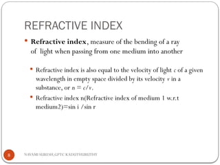
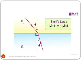
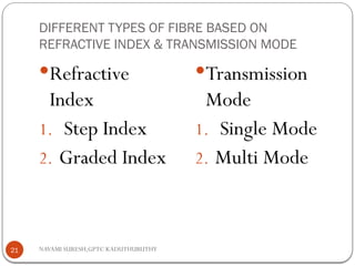
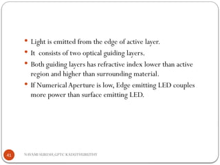
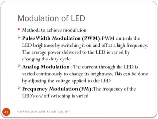
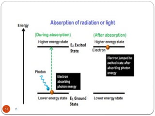
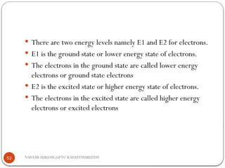
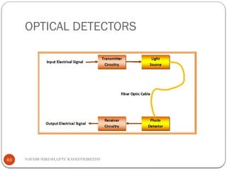
NAVAMI SURESH,GPTC KADUTHURUTHY
SUBMITTED BY,
NAVAMI SURESH
LECTURER IN KADUTHURUTHY
OPTICAL COMMUNICATION
&
NETWORKING
1
NAVAMI SURESH,GPTC KADUTHURUTHY
OPTICAL FIBER COMMUNICATION
 Fiber-optic communication is a method of transmitting
information from one place to another by sending pulses of
light through an optical fiber.
 APPLICATIONS
1. Medical:-Used as light guides, imaging tools and also as
lasers for surgeries
2. Telecommunications- Fiber is laid and used for transmitting
and receiving purposes
3. Used in CCTV surveillance cameras
4. Used in data link for computer networks
2
NAVAMI SURESH,GPTC KADUTHURUTHY
Structure of Optical Fiber
3
NAVAMI SURESH,GPTC KADUTHURUTHY
 Fiber Optic Cable consists of four parts
1. Core
2. Cladding
3. Buffer
4. Jacket
4
NAVAMI SURESH,GPTC KADUTHURUTHY
 Fiber Optic Core: the inner light-carrying member with a high
index of refraction.
 Cladding: the middle layer, which serves to confine the light to
the core. It has a lower index of refraction.
 Buffer:The outer layer, which serves as a "shock absorber" to
protect the core and cladding from damage.The coating usually
comprises one or more coats of a plastic material to protect the
fiber from the physical environment.
 JACKET :Fiber optic cable’s jackets are available in different
colors that can easily make us recognize the exact color of the
cable we are dealing with.
5
NAVAMI SURESH,GPTC KADUTHURUTHY
6
NAVAMI SURESH,GPTC KADUTHURUTHY
REFRACTION
 When a light ray goes from a denser transmission medium
to a rarer one or vice versa, then its direction changes at the
interface of the two medium.This phenomenon is called
refraction of light.
7
NAVAMI SURESH,GPTC KADUTHURUTHY
REFRACTIVE INDEX
 Refractive index, measure of the bending of a ray
of light when passing from one medium into another
 Refractive index is also equal to the velocity of light c of a given
wavelength in empty space divided by its velocity v in a
substance, or n = c/v.
 Refractive index n(Refractive index of medium 1 w.r.t
medium2)=sin i /sin r
8
NAVAMI SURESH,GPTC KADUTHURUTHY
9
NAVAMI SURESH,GPTC KADUTHURUTHY
CRITICAL ANGLE
 Critical angle is defined as the angle of incidence that
provides an angle of refraction of 90-degrees
 sinθc = n2/n1
10
NAVAMI SURESH,GPTC KADUTHURUTHY
Principle of light transmission in a Fiber
 For light propagating from denser medium to rarer medium,
if the angle of refraction is 90 degrees, the corresponding
angle of incidence is called critical angle.
 If a light ray is an incident at the interface of two media with
an angle greater than the critical angle, it is completely
reflected back to the denser medium.This phenomenon is
called total internal reflection.
11
NAVAMI SURESH,GPTC KADUTHURUTHY
12
NAVAMI SURESH,GPTC KADUTHURUTHY
Optical fibers use total internal reflection to transmit
light. It has a solid core of dense glass surrounded by a
less dense cladding.The light ray passing through the
inner core is reflected back instead of being refracted to
the rarer cladding.
13
NAVAMI SURESH,GPTC KADUTHURUTHY
CONDITIONS FOR TOTAL INTERNAL
REFLECTION
 For total internal reflection to take place
(i) light must travel from a denser medium to a rarer medium
(ii) the angle of incidence inside the denser medium must be
greater than the critical angle.
14
NAVAMI SURESH,GPTC KADUTHURUTHY
NUMERICAL APERTURE
 NA is a measure of the light gathering ability of a fiber.
The Numerical Aperture (NA) of a fiber is defined as
the sine of the largest angle an incident ray can have for
total internal reflectance in the core
15
NAVAMI SURESH,GPTC KADUTHURUTHY
ACCEPTANCE ANGLE
 The maximum angle at or below which a ray of light
can enter through one end of the fiber still be total
internal reflection is called as acceptance angle.The
cone is referred as acceptance cone.
16
NAVAMI SURESH,GPTC KADUTHURUTHY
PROBLEMS
 CALCULATETHE SPEED OF LIGHT IN ICE,IF
REFRACTIVE INDEX OF ICE IS 1.31
n=c/v
c=3x10^8 m/s
n=1.31
v=(3x10^8)/1.31
=2.29x10^8m/s
17
NAVAMI SURESH,GPTC KADUTHURUTHY
18
NAVAMI SURESH,GPTC KADUTHURUTHY
19
NAVAMI SURESH,GPTC KADUTHURUTHY
20
NAVAMI SURESH,GPTC KADUTHURUTHY
DIFFERENT TYPES OF FIBRE BASED ON
REFRACTIVE INDEX & TRANSMISSION MODE
Refractive
Index
1. Step Index
2. Graded Index
Transmission
Mode
1. Single Mode
2. Multi Mode
21
NAVAMI SURESH,GPTC KADUTHURUTHY
SINGLE MODE
 Only one path is available.
 Core diameter is small
 Used for long distance communication
 Fabrication is difficult and costly
22
NAVAMI SURESH,GPTC KADUTHURUTHY
Multi Mode
 More than one path is available
 Core radius is larger compared to single mode
 Easy to launch power in to optical fiber
23
NAVAMI SURESH,GPTC KADUTHURUTHY
STEP INDEX FIBER
 The refractive index of the core is uniform throughout and
undergoes on abrupt change at the core cladding boundary
 The path of light propagation is zig- zag in manner
GRADED INDEX FIBER
 The refractive index of the core is made to vary gradually such
that it is maximum at the center of the core.
 The path of light is helical in manner
24
NAVAMI SURESH,GPTC KADUTHURUTHY
25
NAVAMI SURESH,GPTC KADUTHURUTHY
DIFFERENT TYPES OF FIBER MATERIALS
 Optical fibers are used for transmitting light signals over long
distances with minimal loss of signal.They are made from
materials that can guide light effectively.
 The most common materials used for optical fibers are glass
and plastic.
Glass Optical Fibers
 Silica Glass : Most common material due it’s excellent
optical properties, low attenuation, and high-temperature
resistance. Used in most telecommunications and high-speed
data transfer applications
26
NAVAMI SURESH,GPTC KADUTHURUTHY
 Doped Silica: Silica glass doped with materials like
germanium (Ge), phosphorous (P), or boron (B) to modify the
refractive index.
Plastic Optical Fibers
 Polymethyl Methacrylate (PMMA):used in short-
distance applications due to their ease of handling, flexibility,
and lower cost.
 Fluorinated Polymers: These polymers have lower
attenuation than PMMA and are used in specialized applications
requiring higher performance over medium distances
27
NAVAMI SURESH,GPTC KADUTHURUTHY
ADVANTAGES OF OPTICAL FIBERS
1. High Bandwidth: Can transmit significantly higher amounts
of data compared to copper cables.
2. Low Attenuation and Long Distance : Much lower signal
loss
3. High-SpeedTransmission
4. Immunity to Electromagnetic Interference
5. Security : Difficult to tap into a fiber-optic cable without
being detected
6. Easier Installation
7. Lower Operating Costs
28
NAVAMI SURESH,GPTC KADUTHURUTHY
MODULE-2
29
NAVAMI SURESH,GPTC KADUTHURUTHY
OPTICAL SOURCES
 Optical sources refer to devices that emit light or optical
radiation
 FEATURES OF OPTICAL SOURCES
 Size and configuration: Compatible with launching light
into fiber(i.e physical dimensions to suit the optical
fiber).For to couple large amount of power into an optical
fiber, the emitting area should be small.
 High coupling efficiency or have high optical output power
(i.e Adequate output power into the fiber)
30
NAVAMI SURESH,GPTC KADUTHURUTHY
 Narrow spectral width (or line width)
 Stability and efficiency
 The power requirement for its operation must be low.
 High Reliability and low cost
 It must be possible to operate the device continuously at a
variety of temperatures for many years.
31
NAVAMI SURESH,GPTC KADUTHURUTHY
 Main Optical sources for communication are
1. Incoherent sources: Light Emitting
Diode(SLED,ELED,SLD)
2. Coherent Sources : LASER diode(DFB,DBR)
32
NAVAMI SURESH,GPTC KADUTHURUTHY
LIGHT EMITTING DIODE(LED)
 Semiconductor diodes which emits visible or invisible light when
forward biased
 Emits light when voltage is applied
 When forward biased free electrons in the conduction band
recombines with the holes in the valence band and releases
energy in the form of light.
 The process of emitting light in response to the strong electric
field or flow of electric current is called electroluminescence.
 The construction of LED is similar to the normal p-n junction
diode except that gallium, phosphorus and arsenic materials are
used for construction instead of silicon or germanium materials.
33
NAVAMI SURESH,GPTC KADUTHURUTHY
34
NAVAMI SURESH,GPTC KADUTHURUTHY
SYMBOL OF LED
35
NAVAMI SURESH,GPTC KADUTHURUTHY
SURFACE EMITTING & EDGE EMITTING
LEDS
PARAMETER SURFACE EMITTING EDGE EMITTING
Light
Emission
Direction:
Emit light perpendicular to
the surface
Emit light parallel to the surface of the
semiconductor chip
Beam Shape: The light emitted is
usually broad and
somewhat diffuse,
resulting in a wider
beam angle.
narrower beam with higher
directionality.
36
NAVAMI SURESH,GPTC KADUTHURUTHY
PARAMETER SURFACE EMITTING EDGE EMITTING
Applications Commonly used in
indicators, displays, and
lighting applications where a
wide emission pattern is
beneficial.
Commonly used in optical
fiber communications, laser
diodes
Manufacturing: Generally simpler and
cheaper to manufacture
compared to edge-emitting
LEDs
More complex and
expensive to manufacture
Reliability Less Reliable Highly reliable
System Performance Low High
37
NAVAMI SURESH,GPTC KADUTHURUTHY
SURFACE EMITTING LED
38
NAVAMI SURESH,GPTC KADUTHURUTHY
39
NAVAMI SURESH,GPTC KADUTHURUTHY
EDGE EMITTING LED
40
NAVAMI SURESH,GPTC KADUTHURUTHY
 Light is emitted from the edge of active layer.
 It consists of two optical guiding layers.
 Both guiding layers has refractive index lower than active
region and higher than surrounding material.
 If NumericalAperture is low, Edge emitting LED couples
more power than surface emitting LED.
41
NAVAMI SURESH,GPTC KADUTHURUTHY
Modulation of LED
1. Modulating LEDs involves varying their light output by
controlling the electrical input using techniques such as
AM, PWM, and digital modulation.
2. The choice of modulation method depends on the
application requirements, including speed, efficiency, and
complexity.
3. Advances in LED technology and driver circuits continue
to enhance the capabilities and applications of LED
modulation.
42
NAVAMI SURESH,GPTC KADUTHURUTHY
Modulation of LED
 Methods to achieve modulation
 PulseWidth Modulation (PWM):PWM controls the
LED brightness by switching it on and off at a high frequency.
The average power delivered to the LED is varied by
changing the duty cycle
 Analog Modulation :The current through the LED is
varied continuously to change its brightness.This can be done
by adjusting the voltage applied to the LED.
 Frequency Modulation (FM):The frequency of the
LED's on/off switching is varied
43
NAVAMI SURESH,GPTC KADUTHURUTHY
44
NAVAMI SURESH,GPTC KADUTHURUTHY
 Out of these three phenomena transmission and reflection is
of less importance to optical sources and detectors.
 Reflection and transmission are typically considered loss
mechanisms.
45
NAVAMI SURESH,GPTC KADUTHURUTHY
46
NAVAMI SURESH,GPTC KADUTHURUTHY
47
NAVAMI SURESH,GPTC KADUTHURUTHY
48
NAVAMI SURESH,GPTC KADUTHURUTHY
Types of Semiconductors
DIRECT BANDGAP INDIRECT BANDGAP
Generally preferred for
making optical sources.
Cannot be used to
manufacture optical sources.
When an electron
recombines with holes
energy is emitted in form of
light
When an electron
recombines with holes
energy is emitted in form of
light & heat
Example is Gallium
Arsenide (GaAs).
Example is Silicon and
Germanium.
49
NAVAMI SURESH,GPTC KADUTHURUTHY
Theory of Laser action – absorption and emission of
radiation , population inversion, stimulated emission
 LASER is Light Amplification by Stimulated Emission
of Radiation.
 The process by which electrons in the ground state absorbs
energy from external energy sources to vibrate into the
higher energy level is called as absorption.
 Principle of LASER:Absorption and Emission of
Radiation
50
NAVAMI SURESH,GPTC KADUTHURUTHY
51
NAVAMI SURESH,GPTC KADUTHURUTHY
 There are two energy levels namely E1 and E2 for electrons.
 E1 is the ground state or lower energy state of electrons.
 The electrons in the ground state are called lower energy
electrons or ground state electrons
 E2 is the excited state or higher energy state of electrons.
 The electrons in the excited state are called higher energy
electrons or excited electrons
52
NAVAMI SURESH,GPTC KADUTHURUTHY
 When photons or light energy equal to the energy difference
of the two energy levels (E2 – E1) is incident on the atom.
 The ground state electrons gains sufficient energy and
vibrates from ground state (E1) to the excited state (E2).
 Excited state is an unstable state.
 The lifetime of electrons in excited state is of short
period(10 ns).
 After 10 ns, the excited electrons return to the lower energy
state or ground state by releasing energy in the form of
photons
53
NAVAMI SURESH,GPTC KADUTHURUTHY
SPONTANEOUS EMISSION
 This process is a naturally occurring process and is
called as spontaneous emission.
54
NAVAMI SURESH,GPTC KADUTHURUTHY
 But in spontaneous emission no control over excited electron
and it produces incoherent light
 Hence for producing coherent light principle of stimulated
emission is used.
55
NAVAMI SURESH,GPTC KADUTHURUTHY
PRINCIPLE OF LASER
 LASER-LIGHT AMPLIFICATION BY STIMULATED
EMISSION OF RADIATION
 Main principle of LASER IS STIMULATED EMISSION
OF RADIATION
 Stimulated emission involves a process called pumping.
 The electrons in the ground state are vibrated to the excited
states by providing extra energy from energy sources like
electric field(current source) called as electrical pumping
or light called as optical pumping
56
NAVAMI SURESH,GPTC KADUTHURUTHY
STIMULATED EMISSION
57
NAVAMI SURESH,GPTC KADUTHURUTHY
 When incident photon interacts with the excited electron, it
forces the excited electron to return to the ground state
 The excited electron release energy in the form of light while
falling to the ground state
 Two photons are emitted.
 One is due to the incident photon and another one is due to
the energy release of excited electron.
 Hence from one photon, two photons are released.This is
light amplification.
58
NAVAMI SURESH,GPTC KADUTHURUTHY
 All the emitted photons in stimulated emission have the same energy,
same frequency, same polarization and are in phase.
 The number of photons emitted in the stimulated emission depends
on the number of electrons in the higher energy level or excited state
and the incident light intensity.
 The process of achieving greater population in higher energy state
than the lower energy state in order to increase the intensity of light
emitted is called as population inversion.
 To achieve population inversion, atoms must be continuously excited
from a lower energy level to a higher energy level and the process by
which the atoms are excited to a higher energy level is
called pumping.
59
NAVAMI SURESH,GPTC KADUTHURUTHY
LASER diode structure and Radiation
pattern
60
NAVAMI SURESH,GPTC KADUTHURUTHY
 A laser diode is a semiconductor device that transmits
coherent and highly focused light through a process called
stimulated emission.
 It comprises a p-n junction, where electrons and holes
combine, releasing energy as photons.
 The aim of active layer in between p and n-type layers is to
increase the area of electron and hole combination.
 The laser output is taken from active region of the laser
diode.
61
NAVAMI SURESH,GPTC KADUTHURUTHY
62
NAVAMI SURESH,GPTC KADUTHURUTHY
OPTICAL DETECTORS
63
NAVAMI SURESH,GPTC KADUTHURUTHY
PHOTODETECTION
 Photo detector can be defined as a device that is used to detect light
radiations by absorption
 The basic principle of the photo detector is that when an incident
light or radiation falls on the surface of detector and get absorbed, it
converts it into electrical signals.
 Photo detector acts as a reversed biased p-n junction. Let’s
understand how the photo detector works-
 There are three process works in the operation of the photo detector:
 Absorption
 Transportation of Carriers
 Extraction of Carriers As Photocurrent
64
NAVAMI SURESH,GPTC KADUTHURUTHY
 Absorption-In this process, the light energy falls on the photo
detector which gets absorbed by it . Electron-Hole pairs are
generated
 Transportation-In this process, the generated charge carriers
get transported across all the absorption regions.
 Extraction of Carriers As Photocurrent-
 The current is generated mainly because of the photons that
fall on the photo detector, it is called photocurrent.
65
NAVAMI SURESH,GPTC KADUTHURUTHY
PIN Photodiode
66
NAVAMI SURESH,GPTC KADUTHURUTHY
 As the name implies, these photodiodes consist of an un
doped intrinsic layer between two highly doped p-
n junctions.
 Photons hit the intrinsic layer of the PIN diode , they are
absorbed and generate electron-hole pairs. Photons are
absorbed at Intrinsic region .That is the importance of
Intrinsic region.
 The movement of these charge carriers generates a
photocurrent.
 It gives better performance than the common photodiodes.
67
NAVAMI SURESH,GPTC KADUTHURUTHY
68
NAVAMI SURESH,GPTC KADUTHURUTHY
AVALANCHE PHOTODIODE
69
AVALANCHE REGION
INTRINSIC REGION
NAVAMI SURESH,GPTC KADUTHURUTHY
 In the case of p-n photodiodes and p-i-n photodiodes, the output
photocurrent is very small because of the very limited gain.
 To provide a large gain, the avalanche photodiode is used. It is
useful in low light conditions
 Light absorbed in depletion region of P-N junction creating
electron-hole pairs.
 These electron-hole pairs are swept across the depletion region
by reverse bias.
70
NAVAMI SURESH,GPTC KADUTHURUTHY
71
 The key feature of an APD is the high electric field in the
depletion region.As the electron (or hole) accelerates under
this field, it gains enough kinetic energy and collides with
other atoms, creating additional electron-hole pairs.This
process is called Impact Ionization.
 It generates large number of carriers from single photon ,
effectively amplifying signal
NAVAMI SURESH,GPTC KADUTHURUTHY
COMPARE PIN AND AVALANCHE DIODE
PARAMETER PIN DIODE AVALANCHE DIODE
MECHANISM When light strikes the
intrinsic region, electron-
hole pairs are generated
When light generates electron-hole
pairs, the high electric field in the
depletion region causes these carriers
to accelerate and collide with atoms,
creating additional electron-hole
pairs through impact ionization.
RESPONSETIME Faster response since no
multiplication process
involved
Slower response since multiplication
process involved
NOISE Lower noise since there is no
multiplication process
Higher due to avalanche
multiplication process
TEMPERATURE STABILITY Low High
INTERNAL GAIN Low HIGH
REVERSE BIASVOLTAGE Lower Reverse BiasVoltage Higher Reverse biasVoltage
SENSITIVITY Lower since it has no
internal gain
Higher due to avalanche
multiplication process
72

OPTICAL COMMUNICATION AND NETWORKING PRESENTATION

  • 1.
    NAVAMI SURESH,GPTC KADUTHURUTHY SUBMITTEDBY, NAVAMI SURESH LECTURER IN KADUTHURUTHY OPTICAL COMMUNICATION & NETWORKING 1
  • 2.
    NAVAMI SURESH,GPTC KADUTHURUTHY OPTICALFIBER COMMUNICATION  Fiber-optic communication is a method of transmitting information from one place to another by sending pulses of light through an optical fiber.  APPLICATIONS 1. Medical:-Used as light guides, imaging tools and also as lasers for surgeries 2. Telecommunications- Fiber is laid and used for transmitting and receiving purposes 3. Used in CCTV surveillance cameras 4. Used in data link for computer networks 2
  • 3.
  • 4.
    NAVAMI SURESH,GPTC KADUTHURUTHY Fiber Optic Cable consists of four parts 1. Core 2. Cladding 3. Buffer 4. Jacket 4
  • 5.
    NAVAMI SURESH,GPTC KADUTHURUTHY Fiber Optic Core: the inner light-carrying member with a high index of refraction.  Cladding: the middle layer, which serves to confine the light to the core. It has a lower index of refraction.  Buffer:The outer layer, which serves as a "shock absorber" to protect the core and cladding from damage.The coating usually comprises one or more coats of a plastic material to protect the fiber from the physical environment.  JACKET :Fiber optic cable’s jackets are available in different colors that can easily make us recognize the exact color of the cable we are dealing with. 5
  • 6.
  • 7.
    NAVAMI SURESH,GPTC KADUTHURUTHY REFRACTION When a light ray goes from a denser transmission medium to a rarer one or vice versa, then its direction changes at the interface of the two medium.This phenomenon is called refraction of light. 7
  • 8.
    NAVAMI SURESH,GPTC KADUTHURUTHY REFRACTIVEINDEX  Refractive index, measure of the bending of a ray of light when passing from one medium into another  Refractive index is also equal to the velocity of light c of a given wavelength in empty space divided by its velocity v in a substance, or n = c/v.  Refractive index n(Refractive index of medium 1 w.r.t medium2)=sin i /sin r 8
  • 9.
  • 10.
    NAVAMI SURESH,GPTC KADUTHURUTHY CRITICALANGLE  Critical angle is defined as the angle of incidence that provides an angle of refraction of 90-degrees  sinθc = n2/n1 10
  • 11.
    NAVAMI SURESH,GPTC KADUTHURUTHY Principleof light transmission in a Fiber  For light propagating from denser medium to rarer medium, if the angle of refraction is 90 degrees, the corresponding angle of incidence is called critical angle.  If a light ray is an incident at the interface of two media with an angle greater than the critical angle, it is completely reflected back to the denser medium.This phenomenon is called total internal reflection. 11
  • 12.
  • 13.
    NAVAMI SURESH,GPTC KADUTHURUTHY Opticalfibers use total internal reflection to transmit light. It has a solid core of dense glass surrounded by a less dense cladding.The light ray passing through the inner core is reflected back instead of being refracted to the rarer cladding. 13
  • 14.
    NAVAMI SURESH,GPTC KADUTHURUTHY CONDITIONSFOR TOTAL INTERNAL REFLECTION  For total internal reflection to take place (i) light must travel from a denser medium to a rarer medium (ii) the angle of incidence inside the denser medium must be greater than the critical angle. 14
  • 15.
    NAVAMI SURESH,GPTC KADUTHURUTHY NUMERICALAPERTURE  NA is a measure of the light gathering ability of a fiber. The Numerical Aperture (NA) of a fiber is defined as the sine of the largest angle an incident ray can have for total internal reflectance in the core 15
  • 16.
    NAVAMI SURESH,GPTC KADUTHURUTHY ACCEPTANCEANGLE  The maximum angle at or below which a ray of light can enter through one end of the fiber still be total internal reflection is called as acceptance angle.The cone is referred as acceptance cone. 16
  • 17.
    NAVAMI SURESH,GPTC KADUTHURUTHY PROBLEMS CALCULATETHE SPEED OF LIGHT IN ICE,IF REFRACTIVE INDEX OF ICE IS 1.31 n=c/v c=3x10^8 m/s n=1.31 v=(3x10^8)/1.31 =2.29x10^8m/s 17
  • 18.
  • 19.
  • 20.
  • 21.
    NAVAMI SURESH,GPTC KADUTHURUTHY DIFFERENTTYPES OF FIBRE BASED ON REFRACTIVE INDEX & TRANSMISSION MODE Refractive Index 1. Step Index 2. Graded Index Transmission Mode 1. Single Mode 2. Multi Mode 21
  • 22.
    NAVAMI SURESH,GPTC KADUTHURUTHY SINGLEMODE  Only one path is available.  Core diameter is small  Used for long distance communication  Fabrication is difficult and costly 22
  • 23.
    NAVAMI SURESH,GPTC KADUTHURUTHY MultiMode  More than one path is available  Core radius is larger compared to single mode  Easy to launch power in to optical fiber 23
  • 24.
    NAVAMI SURESH,GPTC KADUTHURUTHY STEPINDEX FIBER  The refractive index of the core is uniform throughout and undergoes on abrupt change at the core cladding boundary  The path of light propagation is zig- zag in manner GRADED INDEX FIBER  The refractive index of the core is made to vary gradually such that it is maximum at the center of the core.  The path of light is helical in manner 24
  • 25.
  • 26.
    NAVAMI SURESH,GPTC KADUTHURUTHY DIFFERENTTYPES OF FIBER MATERIALS  Optical fibers are used for transmitting light signals over long distances with minimal loss of signal.They are made from materials that can guide light effectively.  The most common materials used for optical fibers are glass and plastic. Glass Optical Fibers  Silica Glass : Most common material due it’s excellent optical properties, low attenuation, and high-temperature resistance. Used in most telecommunications and high-speed data transfer applications 26
  • 27.
    NAVAMI SURESH,GPTC KADUTHURUTHY Doped Silica: Silica glass doped with materials like germanium (Ge), phosphorous (P), or boron (B) to modify the refractive index. Plastic Optical Fibers  Polymethyl Methacrylate (PMMA):used in short- distance applications due to their ease of handling, flexibility, and lower cost.  Fluorinated Polymers: These polymers have lower attenuation than PMMA and are used in specialized applications requiring higher performance over medium distances 27
  • 28.
    NAVAMI SURESH,GPTC KADUTHURUTHY ADVANTAGESOF OPTICAL FIBERS 1. High Bandwidth: Can transmit significantly higher amounts of data compared to copper cables. 2. Low Attenuation and Long Distance : Much lower signal loss 3. High-SpeedTransmission 4. Immunity to Electromagnetic Interference 5. Security : Difficult to tap into a fiber-optic cable without being detected 6. Easier Installation 7. Lower Operating Costs 28
  • 29.
  • 30.
    NAVAMI SURESH,GPTC KADUTHURUTHY OPTICALSOURCES  Optical sources refer to devices that emit light or optical radiation  FEATURES OF OPTICAL SOURCES  Size and configuration: Compatible with launching light into fiber(i.e physical dimensions to suit the optical fiber).For to couple large amount of power into an optical fiber, the emitting area should be small.  High coupling efficiency or have high optical output power (i.e Adequate output power into the fiber) 30
  • 31.
    NAVAMI SURESH,GPTC KADUTHURUTHY Narrow spectral width (or line width)  Stability and efficiency  The power requirement for its operation must be low.  High Reliability and low cost  It must be possible to operate the device continuously at a variety of temperatures for many years. 31
  • 32.
    NAVAMI SURESH,GPTC KADUTHURUTHY Main Optical sources for communication are 1. Incoherent sources: Light Emitting Diode(SLED,ELED,SLD) 2. Coherent Sources : LASER diode(DFB,DBR) 32
  • 33.
    NAVAMI SURESH,GPTC KADUTHURUTHY LIGHTEMITTING DIODE(LED)  Semiconductor diodes which emits visible or invisible light when forward biased  Emits light when voltage is applied  When forward biased free electrons in the conduction band recombines with the holes in the valence band and releases energy in the form of light.  The process of emitting light in response to the strong electric field or flow of electric current is called electroluminescence.  The construction of LED is similar to the normal p-n junction diode except that gallium, phosphorus and arsenic materials are used for construction instead of silicon or germanium materials. 33
  • 34.
  • 35.
  • 36.
    NAVAMI SURESH,GPTC KADUTHURUTHY SURFACEEMITTING & EDGE EMITTING LEDS PARAMETER SURFACE EMITTING EDGE EMITTING Light Emission Direction: Emit light perpendicular to the surface Emit light parallel to the surface of the semiconductor chip Beam Shape: The light emitted is usually broad and somewhat diffuse, resulting in a wider beam angle. narrower beam with higher directionality. 36
  • 37.
    NAVAMI SURESH,GPTC KADUTHURUTHY PARAMETERSURFACE EMITTING EDGE EMITTING Applications Commonly used in indicators, displays, and lighting applications where a wide emission pattern is beneficial. Commonly used in optical fiber communications, laser diodes Manufacturing: Generally simpler and cheaper to manufacture compared to edge-emitting LEDs More complex and expensive to manufacture Reliability Less Reliable Highly reliable System Performance Low High 37
  • 38.
  • 39.
  • 40.
  • 41.
    NAVAMI SURESH,GPTC KADUTHURUTHY Light is emitted from the edge of active layer.  It consists of two optical guiding layers.  Both guiding layers has refractive index lower than active region and higher than surrounding material.  If NumericalAperture is low, Edge emitting LED couples more power than surface emitting LED. 41
  • 42.
    NAVAMI SURESH,GPTC KADUTHURUTHY Modulationof LED 1. Modulating LEDs involves varying their light output by controlling the electrical input using techniques such as AM, PWM, and digital modulation. 2. The choice of modulation method depends on the application requirements, including speed, efficiency, and complexity. 3. Advances in LED technology and driver circuits continue to enhance the capabilities and applications of LED modulation. 42
  • 43.
    NAVAMI SURESH,GPTC KADUTHURUTHY Modulationof LED  Methods to achieve modulation  PulseWidth Modulation (PWM):PWM controls the LED brightness by switching it on and off at a high frequency. The average power delivered to the LED is varied by changing the duty cycle  Analog Modulation :The current through the LED is varied continuously to change its brightness.This can be done by adjusting the voltage applied to the LED.  Frequency Modulation (FM):The frequency of the LED's on/off switching is varied 43
  • 44.
  • 45.
    NAVAMI SURESH,GPTC KADUTHURUTHY Out of these three phenomena transmission and reflection is of less importance to optical sources and detectors.  Reflection and transmission are typically considered loss mechanisms. 45
  • 46.
  • 47.
  • 48.
  • 49.
    NAVAMI SURESH,GPTC KADUTHURUTHY Typesof Semiconductors DIRECT BANDGAP INDIRECT BANDGAP Generally preferred for making optical sources. Cannot be used to manufacture optical sources. When an electron recombines with holes energy is emitted in form of light When an electron recombines with holes energy is emitted in form of light & heat Example is Gallium Arsenide (GaAs). Example is Silicon and Germanium. 49
  • 50.
    NAVAMI SURESH,GPTC KADUTHURUTHY Theoryof Laser action – absorption and emission of radiation , population inversion, stimulated emission  LASER is Light Amplification by Stimulated Emission of Radiation.  The process by which electrons in the ground state absorbs energy from external energy sources to vibrate into the higher energy level is called as absorption.  Principle of LASER:Absorption and Emission of Radiation 50
  • 51.
  • 52.
    NAVAMI SURESH,GPTC KADUTHURUTHY There are two energy levels namely E1 and E2 for electrons.  E1 is the ground state or lower energy state of electrons.  The electrons in the ground state are called lower energy electrons or ground state electrons  E2 is the excited state or higher energy state of electrons.  The electrons in the excited state are called higher energy electrons or excited electrons 52
  • 53.
    NAVAMI SURESH,GPTC KADUTHURUTHY When photons or light energy equal to the energy difference of the two energy levels (E2 – E1) is incident on the atom.  The ground state electrons gains sufficient energy and vibrates from ground state (E1) to the excited state (E2).  Excited state is an unstable state.  The lifetime of electrons in excited state is of short period(10 ns).  After 10 ns, the excited electrons return to the lower energy state or ground state by releasing energy in the form of photons 53
  • 54.
    NAVAMI SURESH,GPTC KADUTHURUTHY SPONTANEOUSEMISSION  This process is a naturally occurring process and is called as spontaneous emission. 54
  • 55.
    NAVAMI SURESH,GPTC KADUTHURUTHY But in spontaneous emission no control over excited electron and it produces incoherent light  Hence for producing coherent light principle of stimulated emission is used. 55
  • 56.
    NAVAMI SURESH,GPTC KADUTHURUTHY PRINCIPLEOF LASER  LASER-LIGHT AMPLIFICATION BY STIMULATED EMISSION OF RADIATION  Main principle of LASER IS STIMULATED EMISSION OF RADIATION  Stimulated emission involves a process called pumping.  The electrons in the ground state are vibrated to the excited states by providing extra energy from energy sources like electric field(current source) called as electrical pumping or light called as optical pumping 56
  • 57.
  • 58.
    NAVAMI SURESH,GPTC KADUTHURUTHY When incident photon interacts with the excited electron, it forces the excited electron to return to the ground state  The excited electron release energy in the form of light while falling to the ground state  Two photons are emitted.  One is due to the incident photon and another one is due to the energy release of excited electron.  Hence from one photon, two photons are released.This is light amplification. 58
  • 59.
    NAVAMI SURESH,GPTC KADUTHURUTHY All the emitted photons in stimulated emission have the same energy, same frequency, same polarization and are in phase.  The number of photons emitted in the stimulated emission depends on the number of electrons in the higher energy level or excited state and the incident light intensity.  The process of achieving greater population in higher energy state than the lower energy state in order to increase the intensity of light emitted is called as population inversion.  To achieve population inversion, atoms must be continuously excited from a lower energy level to a higher energy level and the process by which the atoms are excited to a higher energy level is called pumping. 59
  • 60.
    NAVAMI SURESH,GPTC KADUTHURUTHY LASERdiode structure and Radiation pattern 60
  • 61.
    NAVAMI SURESH,GPTC KADUTHURUTHY A laser diode is a semiconductor device that transmits coherent and highly focused light through a process called stimulated emission.  It comprises a p-n junction, where electrons and holes combine, releasing energy as photons.  The aim of active layer in between p and n-type layers is to increase the area of electron and hole combination.  The laser output is taken from active region of the laser diode. 61
  • 62.
  • 63.
  • 64.
    NAVAMI SURESH,GPTC KADUTHURUTHY PHOTODETECTION Photo detector can be defined as a device that is used to detect light radiations by absorption  The basic principle of the photo detector is that when an incident light or radiation falls on the surface of detector and get absorbed, it converts it into electrical signals.  Photo detector acts as a reversed biased p-n junction. Let’s understand how the photo detector works-  There are three process works in the operation of the photo detector:  Absorption  Transportation of Carriers  Extraction of Carriers As Photocurrent 64
  • 65.
    NAVAMI SURESH,GPTC KADUTHURUTHY Absorption-In this process, the light energy falls on the photo detector which gets absorbed by it . Electron-Hole pairs are generated  Transportation-In this process, the generated charge carriers get transported across all the absorption regions.  Extraction of Carriers As Photocurrent-  The current is generated mainly because of the photons that fall on the photo detector, it is called photocurrent. 65
  • 66.
  • 67.
    NAVAMI SURESH,GPTC KADUTHURUTHY As the name implies, these photodiodes consist of an un doped intrinsic layer between two highly doped p- n junctions.  Photons hit the intrinsic layer of the PIN diode , they are absorbed and generate electron-hole pairs. Photons are absorbed at Intrinsic region .That is the importance of Intrinsic region.  The movement of these charge carriers generates a photocurrent.  It gives better performance than the common photodiodes. 67
  • 68.
  • 69.
    NAVAMI SURESH,GPTC KADUTHURUTHY AVALANCHEPHOTODIODE 69 AVALANCHE REGION INTRINSIC REGION
  • 70.
    NAVAMI SURESH,GPTC KADUTHURUTHY In the case of p-n photodiodes and p-i-n photodiodes, the output photocurrent is very small because of the very limited gain.  To provide a large gain, the avalanche photodiode is used. It is useful in low light conditions  Light absorbed in depletion region of P-N junction creating electron-hole pairs.  These electron-hole pairs are swept across the depletion region by reverse bias. 70
  • 71.
    NAVAMI SURESH,GPTC KADUTHURUTHY 71 The key feature of an APD is the high electric field in the depletion region.As the electron (or hole) accelerates under this field, it gains enough kinetic energy and collides with other atoms, creating additional electron-hole pairs.This process is called Impact Ionization.  It generates large number of carriers from single photon , effectively amplifying signal
  • 72.
    NAVAMI SURESH,GPTC KADUTHURUTHY COMPAREPIN AND AVALANCHE DIODE PARAMETER PIN DIODE AVALANCHE DIODE MECHANISM When light strikes the intrinsic region, electron- hole pairs are generated When light generates electron-hole pairs, the high electric field in the depletion region causes these carriers to accelerate and collide with atoms, creating additional electron-hole pairs through impact ionization. RESPONSETIME Faster response since no multiplication process involved Slower response since multiplication process involved NOISE Lower noise since there is no multiplication process Higher due to avalanche multiplication process TEMPERATURE STABILITY Low High INTERNAL GAIN Low HIGH REVERSE BIASVOLTAGE Lower Reverse BiasVoltage Higher Reverse biasVoltage SENSITIVITY Lower since it has no internal gain Higher due to avalanche multiplication process 72