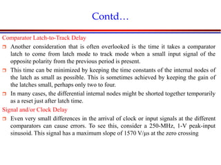
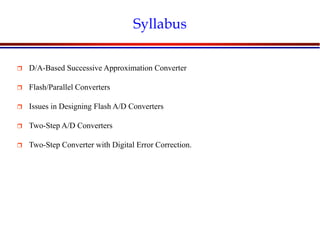
The document provides an overview of Analog-to-Digital Converters (ADCs), particularly focusing on successive approximation and flash converters used in VLSI circuits. It details their operation, advantages, disadvantages, and design considerations, highlighting the importance of factors such as resolution, speed, and power consumption. Additionally, it introduces two-step ADCs as an alternative offering a balance of performance and efficiency in high-speed digital applications.

![Introduction to VLSI Circuits and Systems, NCUT 2007
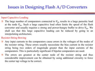
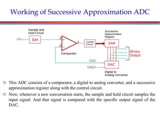
Contd…
Suppose a five-bit SAR ADC. An analog voltage signal of 19 volts is applied at the
input.
Initial Condition
The operation starts by clearing all the bits in SAR. Let’s suppose Q is the output,
since it is a 5-bit ADC, the output will have five bits from Q0 to Q4. Initially, the
contents in successive approximation register (SAR) are given below:
Q = [00000], VDAC = 0V, Vin > VDAC, Vcomp = high](https://image.slidesharecdn.com/module-4-240704091929-d083e500/85/Nyquiest-rate-A-D-conveters-module-4-vasu-5-320.jpg)
![Introduction to VLSI Circuits and Systems, NCUT 2007
Contd…
First Clock Cycle
The comparator output is connected to SAR. As the comparator output goes high,
the device sets the SAR’s most significant bit to one while leaving the other bits at
zero.
Q = [10000], VDAC = 16V, Vin < VDAC, Vcomp = low
Second Clock Cycle
Again, the same procedure will be followed. This time the n-1 bit (that is, the 4th
bit) is set to 1, while all other bits remain unchanged.
Q = [11000], VDAC = 24V, Vin < VDAC, Vcomp = low](https://image.slidesharecdn.com/module-4-240704091929-d083e500/85/Nyquiest-rate-A-D-conveters-module-4-vasu-6-320.jpg)
![Introduction to VLSI Circuits and Systems, NCUT 2007
Contd…
Third Clock Cycle
In this clock cycle, the n-2 bit (that is, the 3rd bit) is set. while the value of the
previous n-1 bit is 0. The value of SAR in the second clock cycle was Q =
[11000] = 24V.
Q = [10100], VDAC = 20V, Vin < VDAC, Vcomp = low
But this value (Q = 10100 or VDAC = 20) is greater than the input voltage.
The approximation is wrong. The output of the comparator goes low.](https://image.slidesharecdn.com/module-4-240704091929-d083e500/85/Nyquiest-rate-A-D-conveters-module-4-vasu-7-320.jpg)
![Introduction to VLSI Circuits and Systems, NCUT 2007
Contd…
Fourth Clock Cycle
In this clock cycle, the n-3 bit (the second bit) is set. while the value of the
previous n-2 bit is 0.
The value of SAR in the third clock cycle was Q = [10100] = 20 V. But this value
is greater than the input voltage. Again, n the approximation is wrong. The n-2 bit
goes low while the n-3 bit goes high.
Q = [10010], VDAC = 18V, Vin < VDAC, Vcomp = high](https://image.slidesharecdn.com/module-4-240704091929-d083e500/85/Nyquiest-rate-A-D-conveters-module-4-vasu-8-320.jpg)
![Introduction to VLSI Circuits and Systems, NCUT 2007
Contd…
Fifth Clock Cycle
In this clock cycle, the n-4 or LSB bit is set. while the other bits remain
unchanged. The value of SAR in the fourth clock cycle was Q = [10010] = 18V.
But this value is less than the input voltage.
The comparator output goes high. The least significant bit goes high.
At the end of the conversion, the input of the DAC is equal to the output of the
DAC.
Q = [10011], VDAC = 19V, End of conversion](https://image.slidesharecdn.com/module-4-240704091929-d083e500/85/Nyquiest-rate-A-D-conveters-module-4-vasu-9-320.jpg)