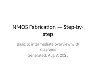
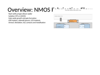
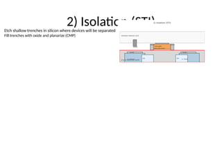
2) Isolation (STI)
Etchshallow trenches in silicon where devices will be separated
Fill trenches with oxide and planarize (CMP)
5.
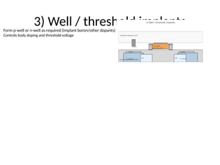
3) Well /threshold implants
Form p-well or n-well as required (implant boron/other dopants)
Controls body doping and threshold voltage
6.
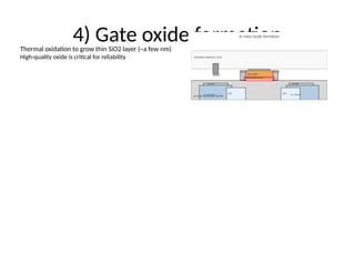
4) Gate oxideformation
Thermal oxidation to grow thin SiO2 layer (~a few nm)
High-quality oxide is critical for reliability
7.
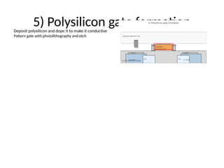
5) Polysilicon gateformation
Deposit polysilicon and dope it to make it conductive
Pattern gate with photolithography and etch
8.
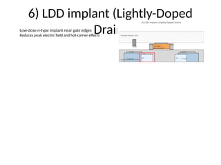
6) LDD implant(Lightly-Doped
Drain)
Low-dose n-type implant near gate edges
Reduces peak electric field and hot-carrier effects
9.
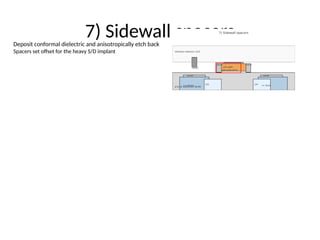
7) Sidewall spacers
Depositconformal dielectric and anisotropically etch back
Spacers set offset for the heavy S/D implant
10.
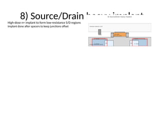
8) Source/Drain heavyimplant
High-dose n+ implant to form low-resistance S/D regions
Implant done after spacers to keep junctions offset
11.
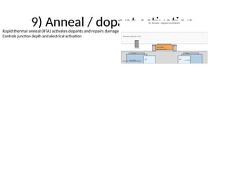
9) Anneal /dopant activation
Rapid thermal anneal (RTA) activates dopants and repairs damage
Controls junction depth and electrical activation
12.
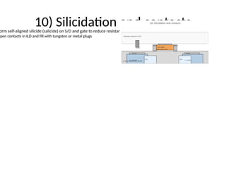
10) Silicidation andcontacts
orm self-aligned silicide (salicide) on S/D and gate to reduce resistance
Open contacts in ILD and fill with tungsten or metal plugs
13.
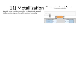
11) Metallization &passivation
Deposit metal interconnects (Al or Cu damascene process)
Add passivation layer and complete back-end processing