1. ICs for Cassette, Cassette Deck
s Overview
The AN6262N and the AN6263N are the pause detec-
tion integrated circuits which select the program on the
cassette tape. In the ordinal method, tape speed is differ-
ent depending on the PLAY and FF/REW, and also non-
signal time between the programs is different. Therefore,
two time constant circuit has been applied in order to
detect each time. The AN6262N and the AN6263N are
proud of detecting the program by making the time corre-
sponding to each non signal time logically in the one time
constant circuit. Furthermore, signal can be detected in
this time constant circuit and beginning of the program is
recognized when sound signal pulse increase more than
specified numbers.
s Features
• Built-in protection circuit to prevent mis-operation when
power switch is turned ON.
• Time-constant circuit for detection of no-signal period
in PLAY and FF/REW.
• No-signal period and output pulse width can be select-
ed by external capacitor.
• Detection level of input signal can be selected by exter-
nal resistor.
• As the ON/OFF input for mode setting and pause
detection, both TTL level and power source level can
be used.
• Very few external components needed.
AN6262N, AN6263N
Pause Detection Circuits of Radio Cassette, Cassette Deck
9
8
7
6
5
4
3
2
0.3 + 0.1
– 0.05
23.3±0.3
6.0±0.3
2.4±0.25
3.3±0.25
1.5±0.25
0.5±0.1
2.54
1.5±0.25
1.4±0.3
3.0±0.3
Unit : mm
30˚
1
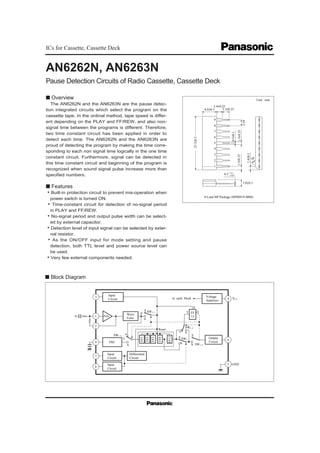
9-Lead SIP Package (SIP009-P-0000)
3 VCC
GND
1
2
9
7
8
6
5
4
Amp.
Input
Circuit
OSC
Input
Circuit
Input
Circuit
Differential
Circuit
Wave
Form
Voltage
Stabilizer
Output
Circuit
FF
13
FF1
FF2
FF8
FF3
FF12
SW1–2
T
b
a
b
P
SW1–1
a
a
a
SW2
b
b
SW1–3
b SW1–4
a
S
QT
Reset
to each block
–
s Block Diagram
2. ICs for Cassette, Cassette DeckAN6262N, AN6263N
*
OFF
FF/REW
PLAY
OFF
Pin No. Pin Name
1
2
3
4
5
6
7
8
9
Signal Input
Negative Feedback
Pause Detection ON/OFF Input
VCC
GND
Output
Mode *
Mode *
Reference Oscillation
s Pin Descriptions
Pin 7
L
H
L
H
Pin 8
L
L
H
H
Mode
16
21
25
336
475
–25 ~ + 75
–55 ~ + 125
VCCSupply Voltage
Supply Current
Power Dissipation
Operating Ambient Temperature
Storage Temperature
V
mA
mA
mW
mW
˚C
˚C
Parameter Unit
s Absolute Maximum Ratings (Ta=25˚C)
AN6262N
AN6263N
AN6262N
AN6263N
ICC
PD
Topr
Tstg
Symbol Rating
Parameter Symbol Condition min. typ. max. Unit
s Electrical Characteristics (VCC=12V, Ta=25˚C)
Supply Current (Output OFF)
Oscillation Frequency
Signal Detection Level
Pause Detection ON/OFF Level
Pause Detection OFF Outcoming Current
Mode Switching
Level
Mode Switching Circuit
Outgoing Current
V3=V7=V8=2V,
V9=1V
V1=0V, V3=V7=V8=0V
f1=10kHz, V3=V7=2V, V8=0V
I3= –100µA, V7=V8=2V, V9=1V
V3=0V, VCC=18V, V7=V8=2V, V9=1V
V3=V8=2V, I7= –100µA, V9=1V
V3=V7=2V, I8= –100µA, V9=1V
V3=V8=2V, VCC=18V, V7=0V, V9=1V
V3=V7=2V, VCC=18V, V8=0V, V9=1V
I4 (OFF)
fOSC
V1
V3–5
I3
V7–5
V8–5
I7
I8
Pin7
Pin8
Pin7
Pin8
AN6262N
AN6263N
11.5
12.5
0.9
1.6
1.1
– 0.6
1.0
1.0
–1.2
–1.2
1.2
20
23
1.47
2.6
1.6
– 0.3
1.5
1.5
– 0.6
– 0.6
mA
mA
kHz
mVrms
V
mA
V
V
mA
mA
t – C
0.01
0.001
0.3
1
3
10
0.003
Oscillation Capacitance C (µF)
Timeofnon-signalperiodt(s)
0.1
0.03
0.01 0.03 0.1 0.3 1
FF/REW
PLAY
OutputPulseW
idth
3. ICs for Cassette, Cassette Deck AN6262N, AN6263N
VCC
(OFF)
1
2
3
4
9
8
7
6
5
–
+
Open (ON)
Search SW
R Ch.
L Ch.
AN6262N
0.027µF
150kΩ
47pF
0.01µF
22kΩ
220kΩ
22kΩ
16V
47µF22kΩ
4.7kΩ
1
2
3
4
9
8
7
6
5
SW (ON)
R Ch.
L Ch.
AN6263N
0.047µF
150kΩ
0.022µF
10kΩ
10kΩ
Open
(OFF)
OpenOpen
–
+16V
47µF
VCC
ON at only
FF/REW
Program detecting circuit only at FF/REW mode.
(1) When the plunger is ON between the program
(2) When the plunger is OFF between the program
s Application Circuits
4. ICs for Cassette, Cassette DeckAN6262N, AN6263N
1) When supply voltage is turned ON and Pin3 is set to “H”
(between the program detection ON), FF1-FF12 are reset and
FF13 is set, Switch SW1 is all connected to a.
2) Mode is set (Pin7 “L”, Pin8 “H”).
3) SW2 is connected to a.
4) Sound signal input to Pin1 becomes pulse after wave
shaped.
5) This sound pulse signal is input to the counter via
SW1-2.
6) Sound pulse signal is input to the counter by 3712
pulses, FF12 is inverted to “H” (L
H
). But no output is
obtained as the SW1– 4 is connected to a.
7) Furthermore sound pulse signal is input by 256, FF12 in
inverted to “L” ( L).
8) When FF12 is inverted from “H” to “L”, FF13 is inverted.
When FF13 is inverted, SW1 is all connected to b.
9) Sound pulse signal, oscillation from oscillator and output of
FF12 are connected to reset pin of the counter, input of the
counter and output circuit, respectively.
10) Counter will count oscillation pulse signal and is reset by
the “H” of sound pulse signal (Program is there).
11) When sound pulse signal is stayed at “L” (program ends),
reset is released. Counter begins to count oscillation pulse
signal and FF12 is inverted to “H” by 3712 pulses.
When static capacitance of the external capacitor at Pin9 is
set to 0.1µF, between the program is detected when no
signal time is more than 3 seconds.
12) Oscillation pulse signal is input furthermore by
256 pulses, FF12 is inverted (“H” “L”), FF13 is
also inverted and SW1 is all connected to a.
13) Returns to 5) mode. Input pulse signal is counted by more
than 3712 + 256 pulses, program is recognized.
s Operational Description
Sound Signal
Pulse
(1) Between the program timing chart (PLAY Mode)
Music MusicPause between the music
(Output polarity is inverted in case of AN6263N)
When sound pulse signal is input by 3712+256
pulses, program is recognized.
Between the program is detected by counting
oscillation pulse signal by 3712 pulses.
3712 Pulse 256 Pulse 3712 Pulse 256 Pulse 3712 Pulse 256 Pulse
(2) Explanation of PLAY mode (Referred to block diagram)
Sound Signal
Reset
Counter Input
FF12
FF13
Output
Oscillation
Signal Pulse
5. ICs for Cassette, Cassette Deck AN6262N, AN6263N
1st music 2nd music
5 sec.
3 sec.
After that, no signal time (more than 3 seconds) comes, between
the program is recognized and output pulse is generated.
If no signal time is less than 3 seconds, it is recognized not
between the program, but program.
Even if noise is contained before more than 3 seconds of 1st
music, between 1st music and 2nd music is detected.
When count of input pulse signal is by less than 3712, it is
recognized as no signal time. So noise is not recognized as
program. Detection of between noise and 1st music is never done.
(3) FF/REW
Mode is set (Pin7 “H”, Pin8 “L”). Switch S2 is connected to
b.
No signal detection time (0.1 seconds) is only different,
count number and pulse width of the sound pulse signal,
which acknowledges program, are the same, and operation is
same, too.
(4) Neither PLAY nor FF/REW
When Pin7, 8 are “H”, “H” and “L” and “L”, between the
program detection is not performed even if between the program
mode is ON.
(5) Switching case of PLAY FF/REW
Always reset and initialized.
(6) Current driving capacitance of the output is minimum 100mA.
When relay is driven directly, equivalent load resistance is most
suitable at 200Ω. (AN6263N).
No signal detection time of PLAY, FF/REW and time of
output pulse width is determined by the relation between
oscillation cycle determined by the oscillation capacitance and
construction stage number of the flip-flop. When oscillation
period is tosc,
Detection time of the PLAY mode : tplay=3712tosc
Detection time of the FF/REW mode : tFF/REW=128tosc
Output pulse width : tout =256tosc
Relation between oscillation cycle and oscillation capacitance is
tosc=8.64C (ms) C : µF,
thus tplay, tFF/REW, tout becomes
tplay=32.07C (s)
tFF/REW=1105.9C (ms)
tout=2211.8C (ms) C : µF.
s How to determine oscillation capacitance
tosc
3712 Pulse
tplay tout
tFF/REW
Oscillation
waveform
Input waveform
(Pin1)
PLAYmode
outputwaveform
(Pin6)
FF/REW mode
outputwaveform
(Pin6)
(Output polarity is inverted in case of AN6263N)
AN6262N
AN6263N
6
Following items should be taken care in order to protect
destruction and keep reliability.
1. Please use it in the absolute maximum ratings. Take care
in case surge voltage shall be applied.
2. Pins except Pin5 should be used in the range of
positive voltage against Pin5.
3. Oscillation capacity should be used with superior thermal
characteristics.
4. When plunger and relay are connected to the output
circuit, diode should be connected to the both side of
coil in order to protect the IC against counter
electromotive force.
s Precautions on Use
VCC