Download as PDF, PPTX


![© 2014 20
Copyrights © Yole Développement SA. All rights reserved.
Terms and Conditions of Sales
Definitions
“Acceptance”: Action by which the Buyer accepts the terms and conditions of sale in their entirety. It is done by signing the purchase order which mentions “I hereby accept Knowmade’s Terms and
Conditions of Sale”.
“Buyer”: Any business user (i.e. any person acting in the course of its business activities, for its business needs) entering into the following general conditions to the exclusion of consumers acting in their
personal interests.
“Contracting Parties” or “Parties”: The Seller on the one hand and the Buyer on the other hand.
“Intellectual Property Rights” (“IPR”) means any rights held by the Seller in its Products, including any patents, trademarks, registered models, designs, copyrights, inventions, commercial secrets and
know-how, technical information, company or trading names and any other intellectual property rights or similar in any part of the world, notwithstanding the fact that they have been registered or not
and including any pending registration of one of the above mentioned rights.
“License”: For the reports and databases, 2 different licenses are proposed. The buyer has to choose one license:
1. Single user license: a single individual at the company can use the report.
2. Corporate license: the report can be used by unlimited users within the company. Subsidiaries are not included.
“Products”: Reports are established in PowerPoint and delivered on a PDF format and the database may include Excel files.
“Seller”: Based in Sophia Antipolis (France headquarters), Knowmade is a technology intelligence company specialized in the research and analysis of scientific and technical information. We provide
patent landscapes and scientific state of the art with high added value to businesses and research laboratories. Our intelligence digests play a key role to define your innovation and development
strategy.
1. Scope
1.1 The Contracting Parties undertake to observe the following general conditions when agreed by the Buyer and the Seller. ANY ADDITIONAL, DIFFERENT, OR CONFLICTING TERMS AND CONDITIONS IN
ANY OTHER DOCUMENTS ISSUED BY THE BUYER AT ANY TIME ARE HEREBY OBJECTED TO BY THE SELLER, SHALL BE WHOLLY INAPPLICABLE TO ANY SALE MADE HEREUNDER AND SHALL NOT BE BINDING
IN ANY WAY ON THE SELLER.
1.2 This agreement becomes valid and enforceable between the Contracting Parties after clear and non-equivocal consent by any duly authorized person representing the Buyer. For these purposes, the
Buyer accepts these conditions of sales when signing the purchase order which mentions “I hereby accept Knowmade’s Terms and Conditions of Sale”. This results in acceptance by the Buyer.
1.3 Orders are deemed to be accepted only upon written acceptance and confirmation by the Seller, within [7 days] from the date of order, to be sent either by email or to the Buyer’s address. In the
absence of any confirmation in writing, orders shall be deemed to have been accepted.
2. Mailing of the Products
2.1 Products are sent by email to the Buyer:
- within [1] month from the order for Products already released; or
- within a reasonable time for Products ordered prior to their effective release. In this case, the Seller shall use its best endeavours to inform the Buyer of an indicative release date and the evolution of
the work in progress.
2.2 Some weeks prior to the release date the Seller can propose a pre-release discount to the Buyer.
The Seller shall by no means be responsible for any delay in respect of article 2.2 above, and including in cases where a new event or access to new contradictory information would require for the
analyst extra time to compute or compare the data in order to enable the Seller to deliver a high quality Products.
2.3 The mailing of the Product will occur only upon payment by the Buyer, in accordance with the conditions contained in article 3.
2.4 The mailing is operated through electronic means either by email via the sales department. If the Product’s electronic delivery format is defective, the Seller undertakes to replace it at no charge to
the Buyer provided that it is informed of the defective formatting within 90 days from the date of the original download or receipt of the Product.
2.5 The person receiving the Products on behalf of the Buyer shall immediately verify the quality of the Products and their conformity to the order. Any claim for apparent defects or for non-conformity
shall be sent in writing to the Seller within 8 days of receipt of the Products. For this purpose, the Buyer agrees to produce sufficient evidence of such defects.
2.6 No return of Products shall be accepted without prior information to the Seller, even in case of delayed delivery. Any Product returned to the Seller without providing prior information to the Seller
as required under article 2.5 shall remain at the Buyer’s risk.](https://image.slidesharecdn.com/reportsamplenanowireledmay2014-140522041238-phpapp01/85/Nanowire-LED-patent-investigation-Sample-20-320.jpg)
![© 2014 21
Copyrights © Yole Développement SA. All rights reserved.
Terms and Conditions of Sales
3. Price, invoicing and payment
3.1 Prices are given in the orders corresponding to each Product sold on a unit basis or corresponding to annual subscriptions. They are expressed to be inclusive of all taxes. The prices may be
reevaluated from time to time. The effective price is deemed to be the one applicable at the time of the order.
3.2 Payments due by the Buyer shall be sent by cheque payable to Knowmade, PayPal or by electronic transfer to the following account:
Banque populaire St Laurent du Var CAP 3000 - Quartier du lac- 06700 St Laurent du Var
BIC or SWIFT code: CCBPFRPPNCE
IBAN: : FR76 1560 7000 6360 6214 5695 126
To ensure the payments, the Seller reserves the right to request down payments from the Buyer. In this case, the need of down payments will be mentioned on the order.
3.3 Payment is due by the Buyer to the Seller within 30 days from invoice date, except in the case of a particular written agreement. If the Buyer fails to pay within this time and fails to contact the
Seller, the latter shall be entitled to invoice interest in arrears based on the annual rate Refi of the «BCE» + 7 points, in accordance with article L. 441-6 of the French Commercial Code. Our publications
(report, database, tool...) are delivered only after reception of the payment.
3.4 In the event of termination of the contract, or of misconduct, during the contract, the Seller will have the right to invoice at the stage in progress, and to take legal action for damages.
4. Liabilities
4.1 The Buyer or any other individual or legal person acting on its behalf, being a business user buying the Products for its business activities, shall be solely responsible for choosing the Products and
for the use and interpretations he makes of the documents it purchases, of the results he obtains, and of the advice and acts it deduces thereof.
4.2 The Seller shall only be liable for (i) direct and (ii) foreseeable pecuniary loss, caused by the Products or arising from a material breach of this agreement
4.3 In no event shall the Seller be liable for:
a) damages of any kind, including without limitation, incidental or consequential damages (including, but not limited to, damages for loss of profits, business interruption and loss of programs or
information) arising out of the use of or inability to use the Seller’s website or the Products, or any information provided on the website, or in the Products;
b) any claim attributable to errors, omissions or other inaccuracies in the Product or interpretations thereof.
4.4 All the information contained in the Products has been obtained from sources believed to be reliable. The Seller does not warrant the accuracy, completeness adequacy or reliability of such
information, which cannot be guaranteed to be free from errors.
4.5 All the Products that the Seller sells may, upon prior notice to the Buyer from time to time be modified by or substituted with similar Products meeting the needs of the Buyer. This modification
shall not lead to the liability of the Seller, provided that the Seller ensures the substituted Product is similar to the Product initially ordered.
4.6 In the case where, after inspection, it is acknowledged that the Products contain defects, the Seller undertakes to replace the defective products as far as the supplies allow and without indemnities
or compensation of any kind for labor costs, delays, loss caused or any other reason. The replacement is guaranteed for a maximum of two months starting from the delivery date. Any replacement is
excluded for any event as set out in article 5 below.
4.7 The deadlines that the Seller is asked to state for the mailing of the Products are given for information only and are not guaranteed. If such deadlines are not met, it shall not lead to any damages or
cancellation of the orders, except for non-acceptable delays exceeding [4] months from the stated deadline, without information from the Seller. In such case only, the Buyer shall be entitled to ask for
a reimbursement of its first down payment to the exclusion of any further damages.
4.8 The Seller does not make any warranties, express or implied, including, without limitation, those of saleability and fitness for a particular purpose, with respect to the Products. Although the Seller
shall take reasonable steps to screen Products for infection of viruses, worms, Trojan horses or other codes containing contaminating or destructive properties before making the Products available, the
Seller cannot guarantee that any Product will be free from infection.
5. Force majeure
The Seller shall not be liable for any delay in performance directly or indirectly caused by or resulting from acts of nature, fire, flood, accident, riot, war, government intervention, embargoes, strikes,
labor difficulties, equipment failure, late deliveries by suppliers or other difficulties which are beyond the control, and not the fault of the Seller.](https://image.slidesharecdn.com/reportsamplenanowireledmay2014-140522041238-phpapp01/85/Nanowire-LED-patent-investigation-Sample-21-320.jpg)

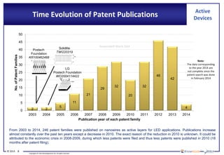
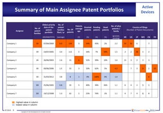
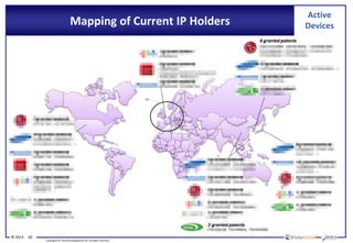
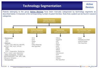
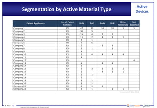
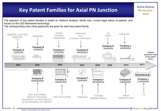
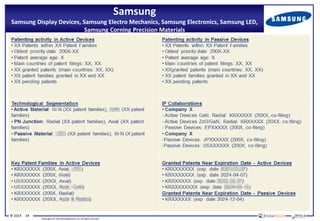
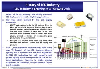
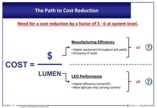
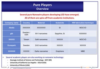
The document outlines a comprehensive report on the patent landscape for LED technology using nanowires, providing insights into the correlation between intellectual property and market trends. It covers over 350 patent families, offering analysis on active and passive devices, key patent holders, and technical segmentation. Additionally, it presents market data, an extensive searchable database of patents, and insights into the evolving LED industry.