Nanowire LED Patent Investigation
New nanowire LED startups compete with Asian LED giants in the IP landscape
KEY FEATURES OF THE REPORT
- Nanowire LED IP landscape
- Focus on key technology issues: deposition method, substrate type, active material type, PN junction type, passive material type
- Main patent applicants' IP collaboration network
- IP collaboration network of main patent applicants
- Matrix patent applicants/technology segments
- Relative strength of main key players' IP
- Key patents and current patents nearing expiration
- "Nanowire LED IP" profiles of six key players incl. their patenting activity, key patents, patented technologies, partnerships, and patents nearing expiration
- Excel database with all patents analyzed incl. technology segmentation
- LED market and industry trends: data and forecasts
- Nanowire LED – Pure-players and their roadmap
Solid electrolytes for lithium ion solid state batteries patent landscape 201...Knowmade
Report’s Key Features
• PDF with > 250 slides
• Excel file > 5,800 patents
• IP trends, including time-evolution of published patents, legal status, countries of patent filings, etc.
• Ranking of main patent assignees
• Patent categorization by type of electrolyte (polymer, inorganic, inorganic/polymer) and inorganic electrolyte materials (sulfide glass ceramics, Thio-LISICON, argyrodite, oxide glass ceramics, NASICON, perovskite, garnet, anti-perovskite, hydride)
• For each technical segment: IP dynamics, ranking of main patent assignees, newcomers, key IP players (leadership, blocking potential, portfolio strength), key patents, and recent development trends
• For each key IP player (100+ companies): Time-evolution of patenting activity, legal status of patents and countries of patent filings, patent segmentation by electrolyte material, IP strengths and weaknesses by electrolyte material
• Excel database containing all patents analyzed in this report, including technology and material segmentations
Microneedles for drug delivery patent landscape 2020 flyerKnowmade
Report’s Key Features
• PDF with > 140 slides
• Excel file > 2,450 patent families
• IP trends, including time-evolution of published patents, and countries of patent filings
• Patents’ legal status
• Ranking of main patent assignees
• Key players’ IP position and relative strength of their patent portfolios
• Summary of the IP related to applications: Cancer therapy, Cosmetic, Diabetes, Ophthalmic, Pain management and Vaccine.
• Summary of the IP related to technologies: Applicators, housing, Coated, Hollow, Porous, Soluble, Hydrogel and Solid microneedles.
• Analysis of patent oppositions (Europe) and review of key patents.
• Excel database containing all patents analyzed in the report, including applications and technologies segmentations
This document provides a summary of a patent landscape analysis report on nanopore sequencing technologies. The analysis found that patent publications on nanopore sequencing have significantly increased from 2008-2013, following early work proving the concept. While industrial players are increasingly active, Harvard University's portfolio remains the strongest, followed by Illumina, Agilent, University of California, and Roche. Oxford Nanopore Technologies' portfolio is not the strongest but the company benefits from university partnerships. Several microelectronics companies have also recently filed solid-state nanopore patents. Most major assignees have an international IP strategy with a strong US and European presence. The report provides a detailed analysis of patents segmented by nanopore technology and application, as well as profiles of key
The presentation introduces the junctionless nanowire transistor biosensor. It works by controlling current flow in a silicon nanowire using a silicon gate separated by an insulating layer. As a biosensor, it can detect positively or negatively charged target molecules binding to receptors on the nanowire, causing a change in conductance. This allows the amount of biomarkers in blood to be quantified. Compared to other technologies, the junctionless nanowire transistor biosensor is faster, uses less power, is simple to build, has reduced costs, and has near-ideal electrical properties.
Nanowire LED Patent Investigation
New nanowire LED startups compete with Asian LED giants in the IP landscape
KEY FEATURES OF THE REPORT
- Nanowire LED IP landscape
- Focus on key technology issues: deposition method, substrate type, active material type, PN junction type, passive material type
- Main patent applicants' IP collaboration network
- IP collaboration network of main patent applicants
- Matrix patent applicants/technology segments
- Relative strength of main key players' IP
- Key patents and current patents nearing expiration
- "Nanowire LED IP" profiles of six key players incl. their patenting activity, key patents, patented technologies, partnerships, and patents nearing expiration
- Excel database with all patents analyzed incl. technology segmentation
- LED market and industry trends: data and forecasts
- Nanowire LED – Pure-players and their roadmap
This document summarizes nanogenerators, which are piezoelectric transducers at the nanoscale that harness mechanical energy and convert it to electrical energy. Dr. Zhong Lin Wang and his colleagues at Georgia Tech have made significant advances in developing nanogenerators using zinc oxide nanowires over the last decade. Nanogenerators consist of a base electrode, piezoelectric nanostructures such as ZnO nanowires, and a counter electrode. When the nanowires are bent or flexed, a voltage is generated via the piezoelectric effect. Nanogenerators have applications powering small electronics and can harvest energy from tiny motions like heartbeats or footsteps.
Next generation power modules - patent landscape 2021 - sampleKnowmade
The advent of EV/HEV technology has acted as a catalyst for innovation, leading to an acceleration in applications for power module related patents since 2010. Who are the main IP players? How do they address the new challenges? Who are the new players and IP challengers taking the big opportunities arising from the emerging EV/HEV market?
KEY FEATURES OF THE REPORT
• IP trends including time evolutions and countries of patent filings
• Current legal status of patents
• Ranking of main patent applicants
• Joint developments and IP collaboration network of main patent applicants
• Key patents and granted patents near expiration
• Relative strength of main companies’ IP portfolios
• Matrix showing patent applicants and their patented technologies
• Segmentation of patents by
- Technology (primary and secondary batteries w/o lithium)
- Design (micro-batteries, solid thin film, flexible, 3D …)
- Components/materials (anode, cathode, electrolyte, barrier layer ...)
- Manufacturing method (CVD, ALD, PVD, sputtering, electrodeposition …)
- Claimed invention (method, product, apparatus)
• Microbattery IP profiles of 10 major companies, with key patents, technological issues, partnerships, IP strength, IP strategy and latest market news
• Excel database with all patents analyzed in the report (3000+ patents), including technology segmentation
Report’s Key Features
• PDF with > 200 slides
• Excel file > 2,500 patents
• IP trends, including time-evolution of published patents, countries of patent filings, etc.
• Patent segmentation per application: Optoelectronics and Photonics, Power, RF, PV and Sensors
• Ranking of main patent assignees
• Key players’ IP position and relative strength of their patent portfolios
• Established players and new entrants
• IP profile of key players, their key patents and their recent IP activity
• Patents recently expired and patents near expiration date
• Excel database containing all patents analyzed in the report, including technology and application segmentations
The report analyzes the patent landscape related to antenna integrated in package (AiP). Over 140 entities have filed AiP patents, with the main assignees being SJ Semiconductor, TSMC, Samsung Electro-Mechanics, Huawei, MediaTek, IBM, ASE, SPIL, NCAP, Qualcomm, and Murata. The report provides a detailed analysis of these players' patent portfolios, technologies, strategies, and key patents. It also includes an Excel database of over 1,500 analyzed AiP patents. The report finds the IP landscape is dominated by foundries/OSATs and major companies, with newcomers being Chinese firms focusing on wafer-level packaging for integrated antennas. The IP
LED phosphor patent investigation 2013 Report by Yole DeveloppementYole Developpement
Phosphor related intellectual property has been and remains a major driving force with strong impact on the shape of the LED industry.
LED phosphor IP is shaping the industry
The first commercial GaN-based blue LEDs were produced in Japan in the mid 90’s after researchers Shuji Nakamura at Nichia and Professor Akasaki at Nagoya University (IP assigned to Toyoda Gosei) succeeded in removing some of the major remaining roadblocks associated with this technology (p-doping, epitaxy quality…).
Quickly leveraging on this success, some fundamental patents describing the use of a blue LED combined with a phosphor to produce white LEDs were filed by Nichia, Osram, ATMI and others. Those fundamental patents were rapidly followed by a fast growing number of applications through 2005 as an increasing number of companies started to compete in the LED market and new applications in cell phone, laptop and LCD TV display, and general lighting were being addressed.
Phosphor IP is a major force in the LED industry. With more than 40 litigation cases, it is also used as leverage by companies which have negotiated close to 70 licensing and supply agreements to date. It can also be argued that in the first half of the 2000 decade, the strict enforcement and lack of license grants for some fundamental IP related to the design and manufacturing of white LEDs might also have slowed down the progress of the industry by preventing more efficient competition that would allow prices to decrease.
The report identifies the key players with the most relevant IP. It provides an overview, of phosphor related IP litigation and licensing, that has shaped the industry since the mid 90s, as well as a detailed analysis for the major players involved.
A vast number of relevant patents
Our search strategy combines automated and manual screenings that have led to the selection of more than 4,500 relevant patent families. Those have been segmented by type (composition patent or phosphor configuration patents) and organized in various technology segments that are analyzed in detail: garnets, silicates, nitrides and oxynitrides, quantum dots. The report also includes a special focus on the emerging LED phosphor IP in China.
For each segment, the report provides a detailed analysis including the time evolution of patent filings, identification of the key players, collaborations and citation networks, as well as the identification of the key patents based-on citation and impacts in litigations.
The report also includes a companion excel database with all patents of the company profiled in the report. This database includes abstracts and hyperlinks to the original documents and allows multi-criteria searches (patent publication number, priority date, title, applicants, technological segments…)
More information on the report at http://www.i-micronews.com/reports/LED-Phosphors-Down-Converters-Patent-Investigation/14/392/
Group III nitride semiconductors are recognized as having great potential for short wave length emission (LEDs, LDs, UV detectors) and high-temperature electronics devices. The field of III-N semiconductors has shown an intensive patenting activity since early 1990s, with a substantial increase during the past decade. Today, there are more than 27,000 patent families filed all over the world. The most active companies are Panasonic, Toshiba, Samsung, Sumitomo and Hitachi. The patents related to LED technology account for more than 40% of filings, followed by those related to GaN substrates (5%) and RF & Advanced Electronics (<5%).
More than 1,570 new patent families were published between early April 2012 and late March 2013. They were filed by about 350 patent applicants mainly located in Japan, Korea, USA and China. The main patent applicants are Sumitomo, Toshiba, Samsung, Sharp and Mitsubishi which represent together almost 25% of the patents published the last 12 months. The academic organisms account for almost 15% of new patent filings and they are mainly located in China. The data set was segmented by type of application (Substrates, Epi-wafers, LED & Laser, Power Devices, RF & Advanced Electronics, Photovoltaics, Sensors-Detectors-MEMS). About 45% of new patent families published the last 12 months are related to LED technology.
They were mainly filed by Toshiba, LG and Samsung, while Chinese companies are increasing their patent activity (Tongfang, Sanan Optoelectronics). The patents claiming an invention related to III-N Substrates and Power Devices represent 20% and 14% of new filings respectively. The patents dedicated to Substrate technology were mainly filed by Sumitomo, Hitachi and Mitsubishi, while University of California and Soitec filed 15 and 8 new patents respectively. The patents dedicated to Power Devices were mainly filed by Advanced Power Device Research Association, Samsung and Sumitomo and the patent filings remain dominated by Japanese companies. Numerous patent applications published this year are offered for sale or for license. This year, the most relevant offers are the ones from the University of California (e.g. Ammonothermal growth technique, CAVET for High Power Application, Defect reduction of semi-polar III-N, GaN substrates, III-N tandem solar cells .
Report’s Key Features
• PDF with > 310+ slides
• Identification of the startups that recently started to work in the field of Microfluidics
• Mapping of the new startups
• Segmentation by technology and application
• Focused analysis of the projects aiming at Oncology, Diabetes and Neurology.
• Description of the startups and their microfluidic-related projects
• Presentation of all their published patent families.
• Description of key people and their background.
• Excel database containing all patents analyzed in the report
Miniaturized Gas Sensors Patent Landscape 2016 SampleKnowmade
KEY FEATURES OF THE REPORT
• IP trends including time evolutions and countries of patent filings
• Current legal status of patents
• Ranking of main patent applicants
• Joint developments and IP collaboration network of main patent applicants
• Key patents and granted patents near expiration
• Relative strength of main companies’ IP portfolios
• Matrix showing patent applicants and their patented technologies
• Segmentation of patents by gas sensor technology: Electrical detector (FET, CMOS, MOS/MIS), chemical sensor, optical detector, acoustic detector, gas chromatography, electro-chemical gas sensor, thermal gas sensor, gas sensor with CNTs/Graphene, electro-mechanical gas sensors
• IP position vs. market positions for each key players
• MEMS gas sensor IP profiles of 19 key companies, with key patents, technological issues, partnerships, IP strength, IP strategy and latest market news
• Excel database with all patents analyzed in the report (2000+ patents), including technology segmentation
This power point presentation talks about key firms that are involved in LED phosphor industry and the strategy adopted by them. This presentaion is based on NanoMarkets' report "LED Phosphor Markets-2014"
Yole led phosphor_qd_ip_january_2016_sampleClotilde Fabre
This document provides an overview of the patent landscape report on phosphors and quantum dots for LED applications. The report analyzes over 7,500 relevant patent families and provides an in-depth examination of the major patent holders, key technologies, litigation and licensing activities, and emerging trends. It identifies the leading companies in different patent segments, such as phosphor compositions and quantum dots, and analyzes the strengths and weaknesses of their intellectual property portfolios.
Power GaN 2016: Epitaxy and Devices, Applications, and Technology Trends - 20...Yole Developpement
GaN power devices: a promising, fast-growing market
A GROWING MARKET WITH LOTS OF EXCITING NEWS IN 2015 - 2016
2015 - 2016 has been an exciting year for the gallium nitride (GaN) power business. Up until late 2014, 600V/650V GaN HEMTs’ commercial availability was still questionable, despite some announcements from different players. Fast-forward to 2016 end users can now buy not only low-voltage GaN (<200V) devices from Efficient Power Conversion (EPC), but also high-voltage (600V/650V) components from several players, including Transphorm, GaN Systems, and Panasonic.
Also, a new start-up, Navitas Semiconductor, announced their GaN power IC in March 2016, followed by Dialog Semiconductors revealing their GaN power IC in August 2016. The idea
of bringing GaN from the power semiconductor market to the much bigger analog IC market is of interest to several other players too. For example, EPC and GaN Systems are both working on a more integrated solution, and Texas Instruments, a well-established analog IC player, has also been engaged in GaN activities, releasing an 80V power stage and 600V power stage in 2015 and 2016, respectively.
Despite these exciting developments, the GaN power market remains small compared to the gigantic $335B silicon semiconductor market. In fact, according to Yole Développement (Yole) investigation the GaN power business was less than $10M in 2015. But before you think twice about GaN, remember that a small market size is not unusual for products just appearing on the market.
The first GaN devices were not commercially available until 2010, so we are talking about an industry that is only six years old. What is most important is the GaN market’s future potential – and Yole expects the GaN power business to grow, reaching a market size of around $300M in 2021 at a 2016 – 2021 CAGR of 86%.
This report provides a structured vision of the GaN power device market in terms of uses, applications, and potential trends.
Consumer Physics Inc. develops and distributes molecular sensors, marketing its product under the SCiO brand name. According to Consumer Physics, the SCiO spectrometer is the world’s first pocket size molecular sensor. The company had over 13,000 backers on Kickstarter and ended up raising over $2.7 million. Consumers can use SCiO to scan objects including fruit, vegetables, dairy food, meat, fish and medications. They can even scan their own bodies to measure total body fat. The SCiO app also includes a DIY applet that allows anyone to scan materials of their choosing and analyze the difference between their molecular identities. Consumer Physics has won numerous awards including an ‘Enabled by Optics’ award from OSA, The Optical Society, in 2016, the World Economic Forum Technology Pioneers Award 2015, the United Nations Netexplo Award 2015 and was a CES Innovation Honoree in 2016. SCiO has regularly appeared in top ‘products to watch’ lists on Forbes, CNN, and Fortune, and has been covered numerous times by the media on television, in print and online. But what technologies are behind Consumer Physics’ success and what are the main features claimed by its patents?
Photolithography Equipment and Materials for Advanced Packaging, MEMS and LED...Yole Developpement
Growing photolithography equipment markets in Advanced Packaging, MEMS and LEDs are attracting new players – but they have to navigate complex roadmaps.
Clear leaders and outsiders: At first glance, the projection systems industry serving the “More Moore” and the “More than Moore” markets are similar…
The semiconductor industry is very often identified by its “More Moore” players, driven by technology downscaling and cost reduction. There’s one clear leader supplying photolithography tools to the “More Moore” industry: ASML, based in The Netherlands. It’s followed by two Japanese outsiders, Nikon and Canon. Providing this market with photolithography equipment is highly complex and there are gigantic barriers to market entry. Enormous R&D investments are required as the key features to print shrink ever further. Also, the tolerances specified are very aggressive and thus equipment complexity keeps on increasing...
Next generation power modules - patent landscape 2021- flyerKnowmade
The advent of EV/HEV technology has acted as a catalyst for innovation, leading to an acceleration in applications for power module related patents since 2010. Who are the main IP players? How do they address the new challenges? Who are the new players and IP challengers taking the big opportunities arising from the emerging EV/HEV market?
Antenna for 5G patent landscape 2019 flyerKnowmade
Report’s Key Features
• PDF >120 slides
• Excel file >3,600 patents
• IP trends, including time-evolution of published patents, and countries of patent filings
• Ranking of main patent assignees
• Patent analysis for main applications (handsets, infrastructures & networks, vehicles) and technologies (MIMO, beamforming, antenna array, mm-wave, monopole antenna, dipole antenna, microstrip antenna, etc.)
• Key patents
• Key players’ IP position, and relative strength of their patent portfolios
• Key players’ IP profile: Samsung Electronics, Oppo Mobile, Huawei, and Intel
• Excel database containing all patents analyzed in this report, including technology and application segmentations
SCiO Molecular Sensor from Consumer Physics: Mobile Spectrometer Dongle - tea...Yole Developpement
The world’s first pocket-sized molecular sensor that can be integrated into consumer smartphones
For a long time, spectral analysis of materials has been limited to academic research. Everyday application of this type of analysis could bring new interactions in areas including food, fitness and medication. Starting with a crowdfunding campaign, and following the path of companies like FLIR, Consumer Physics, which was formerly Verifood Ltd., has created the first dongle molecular sensor, the SCiO Spectrometer. Thanks to big data and cloud technology, the dongle spectrometer claims to take the spectral fingerprint of any substance and quantify or identify any compound.
Consumer Physics is the first to bring spectrometry to consumers. Unlike other spectrometers, Consumer Physics produces a very simple package based on a tiny spectrometer head, with an area of 13 mm x 19 mm.
The SCiO Spectrometer integrates a 1.2 M pixel monochromatic CMOS image sensor from ON Semiconductor, a white LED from OSRAM and a bespoke filter/lens array. The LED is coupled to a reflector in the illumination module, which shines light on the analyzed substance, whose molecules absorb specific wavelengths. The received light in the spectrometer module is filtered and broken up into different wavelengths by the various lenses. Finally, the image sensor gives an instant response from the analyzed substance.
For more information please visit our website: http://www.i-micronews.com/reports.html
IEEE Digital Senses Initiative - Standards Activities 3/30/2017yymedia
IEEE Digital Senses Initiative is an IEEE “future directions” initiative dedicated to hacking human senses for VR, AR and human augmentation.
IEEE P2048 Working Group is developing eight standards for virtual reality (VR) and augmented reality (AR). Having attracted participants from 194 companies and institutions all over the world, the working group now is one of the largest forces dedicated to VR/AR standardization. The working group participants already include device manufacturers, content providers, service providers, technology developers, government agencies and other parties relevant to VR/AR, constituting an excellent mixture for the standards to be widely adopted.
Market & Technology Trends in Materials and Equipement for Printed and Flexib...Yole Developpement
Combined flexible & printed electronic applications could reach US$1B in 2020. Multiple applications are driving growth!
TECHNICAL CHALLENGES ARE CLOSE TO BEING OVERCOME TO REACH US$1B MARKET BY 2020
Today flexible & printed electronics create a lot of hope. And a supply chain is being created to support an industrial infrastructure. In our report, we have identified and tracked the five main functionalities of flexible & printed electronics: displaying, sensing, lighting, energy generating and substrates. The different degrees of freedom in flexibility that can be obtained can be divided into:
- Conformable substrate: the flexible substrate will be shaped in a definitive way after processing
- “Bendable” substrate: they can be rolled and bent many times (even if we consider it will not be a key feature coming from customer needs)
- “Unused” flexibility: in the end, the flexibility is not an added value to the customer
We believe some applications will be more likely than other to be successful – for example, bendable applications will undergo tough stress during use and technological challenges will be hard to overcome. Our report shows the distinction between the functions (displaying, lighting, energy conversion, sensing & substrates) and the seek flexibility “degree of freedom”. We do not make the distinction in our report between organic and inorganic substrates as semiconductors can also be used as flexible substrates.
However, we believe over the next several years, the number of applications using printing processes for flexible electronics will grow (Figure on page 2).
We estimate the printed & flexible electronics market will grow from ~ $176M in 2013 to ~$950M in 2020 with a 27% CAGR in market value. Printed OLED displays for large size (TVs) are likely to become the largest market. For OLED lighting, we believe it will grow but remain a niche market for automotive and/ or office lighting. For PV, the market demand by 2020 will remain very low compared to the demand for rigid PV, largely below 1% of the global market demand by 2020. Sensor, smart system & polytronic applications will include sensors, touchless / touch screens, RF ID applications.
A WIDE, EXCITING RANGE OF NEW APPLICATIONS
Printed & flexible electronics is a new exiting technology with large potential market expectations. Indeed, as semiconductors move to the very small with 22nm critical dimension, printed electronics moves to the other end of the spectrum with its own material, equipment, process challenges and supply chain. Printed electronics will not kill semiconductor electronics as it will not be a replacement for CMOS silicon.
More info at http://www.i-micronews.com/reports/Flexible-Based-Printed-Electronics-Technologies/6/367/
GaN Technology Top-100 IP profiles - SampleKnowmade
The field of III-N semiconductors has shown an intensive patenting activity since early 1990s, with a substantial increase during the past decade. Today, more than 76,200 patents and patent applications related to over 39,700 inventions on GaN technology have been published worldwide through November 2016. This fact is correlated with a rapid growth of the industrial activity related to GaN, mainly due to light-emitting diodes, but also to the emergence of lasers and high-power/high-frequency electronics. Moreover, the current diversification of GaN-related research activities is remarkable, ranging from advanced optical sources and single-electron devices to physical, chemical, and biological sensors, optical detectors, and energy converters. In this dynamic and large context, it is necessary to have a clear overview of main companies and research laboratories involved in this technology domain.
The report provides essential patent data for IP players related to GaN technology. It identifies 100 major patent holders involved in GaN technology, and its provides in a single slide the IP profile of each main patent holder including: time evolution of patent publications, geographic map of patenting activity, technical segments, highly cited patents, main IP competitors and IP collaborators.
Advanced Substrates Overview: From IC Package to Board - 2017 Report by Yole ...Yole Developpement
How can advanced substrates and boards bridge the gap created by front-end scaling?
Advanced substrates as a key enabler of future products and markets
In an uncertain, transformative semiconductor market, advanced packaging is one of the key technologies offering stability and a long-term solution. On one hand it can adapt to product diversification, offering more functionality, system integration, and performance, as well as potentially lower manufacturing cost; and on the other hand it can adhere to future scaling requirements. Advanced substrates are the key interconnect component of advanced packaging architectures and are critical in enabling future products and markets. For this reason, Yole has established this stand-alone dedicated advanced substrate activity, focused on exploring the market and technologies of PCBs, package substrates and RDLs. This first report will serve as an overview of advanced substrate technologies, markets, and supply chain, to be supported by subsequent in-depth reports.
Today’s advanced substrates in volume are Flip Chip (FC) substrates, 2.5D/3D TSV assemblies, and thin-film RDLs (Fan-Out WLP, or “FOWLP”) below an L/S resolution of 15/15 um and with transition below L/S < 10/10 um. These advanced substrates are traditionally linked to higher-end logic (CPUs/GPUs, DSPs, etc.) driven by ICs in the latest technology nodes in the computing, networking, mobile, and high-end consumer market segments (gaming, HD/Smart TV). However, due to additional form factor and low power demands, WLP and advanced FC substrates are also widespread in majority of smartphone functions: application processors, baseband, transceivers, filters, amplifiers, WiFi modules, drivers, codecs, power management, etc.
For more information, please visit our website: http://www.i-micronews.com/reports.html
Report’s Key Features
• PDF with > 230 slides
• Excel file > 3,000 patent families
• Main IP dynamics and key trends.
• IP leaders, most active players and newcomers.
• IP portfolio strength of key players, and their technology/application focus.
• Time evolution of patents filings by company, countries, and technology.
• IP collaborations and IP transfers between key organizations.
• Insights into the status of RF GaN patented technologies, identifying trends for each technology and application.
• Extensive Excel database of over 3,000 patent families with all patent information and technology segmentation.
Cancer diagnostics startup identification 2020 sampleKnowmade
Report’s Key Features
• PDF with > 430+ slides
• Identification & mapping of the startups that recently started to work in the field of cancer diagostics.
• Identification & mapping of the startups that recently started to work in the field of cancer diagnostics.
• Segmentation by technology (Medical imaging, Software, AI-based tool, Biochemical analysis, Molecular diagnostics, Lab-on-chip, Liquid biopsy etc.)
• Description of the startups and their current stage of product development, funding rounds and subsidies.
• Presentation of all their relevant published patent families.
• Description of key people and their background.
More Related Content
Similar to Nanowire LED patent investigation Flyer
Report’s Key Features
• PDF with > 200 slides
• Excel file > 2,500 patents
• IP trends, including time-evolution of published patents, countries of patent filings, etc.
• Patent segmentation per application: Optoelectronics and Photonics, Power, RF, PV and Sensors
• Ranking of main patent assignees
• Key players’ IP position and relative strength of their patent portfolios
• Established players and new entrants
• IP profile of key players, their key patents and their recent IP activity
• Patents recently expired and patents near expiration date
• Excel database containing all patents analyzed in the report, including technology and application segmentations
The report analyzes the patent landscape related to antenna integrated in package (AiP). Over 140 entities have filed AiP patents, with the main assignees being SJ Semiconductor, TSMC, Samsung Electro-Mechanics, Huawei, MediaTek, IBM, ASE, SPIL, NCAP, Qualcomm, and Murata. The report provides a detailed analysis of these players' patent portfolios, technologies, strategies, and key patents. It also includes an Excel database of over 1,500 analyzed AiP patents. The report finds the IP landscape is dominated by foundries/OSATs and major companies, with newcomers being Chinese firms focusing on wafer-level packaging for integrated antennas. The IP
LED phosphor patent investigation 2013 Report by Yole DeveloppementYole Developpement
Phosphor related intellectual property has been and remains a major driving force with strong impact on the shape of the LED industry.
LED phosphor IP is shaping the industry
The first commercial GaN-based blue LEDs were produced in Japan in the mid 90’s after researchers Shuji Nakamura at Nichia and Professor Akasaki at Nagoya University (IP assigned to Toyoda Gosei) succeeded in removing some of the major remaining roadblocks associated with this technology (p-doping, epitaxy quality…).
Quickly leveraging on this success, some fundamental patents describing the use of a blue LED combined with a phosphor to produce white LEDs were filed by Nichia, Osram, ATMI and others. Those fundamental patents were rapidly followed by a fast growing number of applications through 2005 as an increasing number of companies started to compete in the LED market and new applications in cell phone, laptop and LCD TV display, and general lighting were being addressed.
Phosphor IP is a major force in the LED industry. With more than 40 litigation cases, it is also used as leverage by companies which have negotiated close to 70 licensing and supply agreements to date. It can also be argued that in the first half of the 2000 decade, the strict enforcement and lack of license grants for some fundamental IP related to the design and manufacturing of white LEDs might also have slowed down the progress of the industry by preventing more efficient competition that would allow prices to decrease.
The report identifies the key players with the most relevant IP. It provides an overview, of phosphor related IP litigation and licensing, that has shaped the industry since the mid 90s, as well as a detailed analysis for the major players involved.
A vast number of relevant patents
Our search strategy combines automated and manual screenings that have led to the selection of more than 4,500 relevant patent families. Those have been segmented by type (composition patent or phosphor configuration patents) and organized in various technology segments that are analyzed in detail: garnets, silicates, nitrides and oxynitrides, quantum dots. The report also includes a special focus on the emerging LED phosphor IP in China.
For each segment, the report provides a detailed analysis including the time evolution of patent filings, identification of the key players, collaborations and citation networks, as well as the identification of the key patents based-on citation and impacts in litigations.
The report also includes a companion excel database with all patents of the company profiled in the report. This database includes abstracts and hyperlinks to the original documents and allows multi-criteria searches (patent publication number, priority date, title, applicants, technological segments…)
More information on the report at http://www.i-micronews.com/reports/LED-Phosphors-Down-Converters-Patent-Investigation/14/392/
Group III nitride semiconductors are recognized as having great potential for short wave length emission (LEDs, LDs, UV detectors) and high-temperature electronics devices. The field of III-N semiconductors has shown an intensive patenting activity since early 1990s, with a substantial increase during the past decade. Today, there are more than 27,000 patent families filed all over the world. The most active companies are Panasonic, Toshiba, Samsung, Sumitomo and Hitachi. The patents related to LED technology account for more than 40% of filings, followed by those related to GaN substrates (5%) and RF & Advanced Electronics (<5%).
More than 1,570 new patent families were published between early April 2012 and late March 2013. They were filed by about 350 patent applicants mainly located in Japan, Korea, USA and China. The main patent applicants are Sumitomo, Toshiba, Samsung, Sharp and Mitsubishi which represent together almost 25% of the patents published the last 12 months. The academic organisms account for almost 15% of new patent filings and they are mainly located in China. The data set was segmented by type of application (Substrates, Epi-wafers, LED & Laser, Power Devices, RF & Advanced Electronics, Photovoltaics, Sensors-Detectors-MEMS). About 45% of new patent families published the last 12 months are related to LED technology.
They were mainly filed by Toshiba, LG and Samsung, while Chinese companies are increasing their patent activity (Tongfang, Sanan Optoelectronics). The patents claiming an invention related to III-N Substrates and Power Devices represent 20% and 14% of new filings respectively. The patents dedicated to Substrate technology were mainly filed by Sumitomo, Hitachi and Mitsubishi, while University of California and Soitec filed 15 and 8 new patents respectively. The patents dedicated to Power Devices were mainly filed by Advanced Power Device Research Association, Samsung and Sumitomo and the patent filings remain dominated by Japanese companies. Numerous patent applications published this year are offered for sale or for license. This year, the most relevant offers are the ones from the University of California (e.g. Ammonothermal growth technique, CAVET for High Power Application, Defect reduction of semi-polar III-N, GaN substrates, III-N tandem solar cells .
Report’s Key Features
• PDF with > 310+ slides
• Identification of the startups that recently started to work in the field of Microfluidics
• Mapping of the new startups
• Segmentation by technology and application
• Focused analysis of the projects aiming at Oncology, Diabetes and Neurology.
• Description of the startups and their microfluidic-related projects
• Presentation of all their published patent families.
• Description of key people and their background.
• Excel database containing all patents analyzed in the report
Miniaturized Gas Sensors Patent Landscape 2016 SampleKnowmade
KEY FEATURES OF THE REPORT
• IP trends including time evolutions and countries of patent filings
• Current legal status of patents
• Ranking of main patent applicants
• Joint developments and IP collaboration network of main patent applicants
• Key patents and granted patents near expiration
• Relative strength of main companies’ IP portfolios
• Matrix showing patent applicants and their patented technologies
• Segmentation of patents by gas sensor technology: Electrical detector (FET, CMOS, MOS/MIS), chemical sensor, optical detector, acoustic detector, gas chromatography, electro-chemical gas sensor, thermal gas sensor, gas sensor with CNTs/Graphene, electro-mechanical gas sensors
• IP position vs. market positions for each key players
• MEMS gas sensor IP profiles of 19 key companies, with key patents, technological issues, partnerships, IP strength, IP strategy and latest market news
• Excel database with all patents analyzed in the report (2000+ patents), including technology segmentation
This power point presentation talks about key firms that are involved in LED phosphor industry and the strategy adopted by them. This presentaion is based on NanoMarkets' report "LED Phosphor Markets-2014"
Yole led phosphor_qd_ip_january_2016_sampleClotilde Fabre
This document provides an overview of the patent landscape report on phosphors and quantum dots for LED applications. The report analyzes over 7,500 relevant patent families and provides an in-depth examination of the major patent holders, key technologies, litigation and licensing activities, and emerging trends. It identifies the leading companies in different patent segments, such as phosphor compositions and quantum dots, and analyzes the strengths and weaknesses of their intellectual property portfolios.
Power GaN 2016: Epitaxy and Devices, Applications, and Technology Trends - 20...Yole Developpement
GaN power devices: a promising, fast-growing market
A GROWING MARKET WITH LOTS OF EXCITING NEWS IN 2015 - 2016
2015 - 2016 has been an exciting year for the gallium nitride (GaN) power business. Up until late 2014, 600V/650V GaN HEMTs’ commercial availability was still questionable, despite some announcements from different players. Fast-forward to 2016 end users can now buy not only low-voltage GaN (<200V) devices from Efficient Power Conversion (EPC), but also high-voltage (600V/650V) components from several players, including Transphorm, GaN Systems, and Panasonic.
Also, a new start-up, Navitas Semiconductor, announced their GaN power IC in March 2016, followed by Dialog Semiconductors revealing their GaN power IC in August 2016. The idea
of bringing GaN from the power semiconductor market to the much bigger analog IC market is of interest to several other players too. For example, EPC and GaN Systems are both working on a more integrated solution, and Texas Instruments, a well-established analog IC player, has also been engaged in GaN activities, releasing an 80V power stage and 600V power stage in 2015 and 2016, respectively.
Despite these exciting developments, the GaN power market remains small compared to the gigantic $335B silicon semiconductor market. In fact, according to Yole Développement (Yole) investigation the GaN power business was less than $10M in 2015. But before you think twice about GaN, remember that a small market size is not unusual for products just appearing on the market.
The first GaN devices were not commercially available until 2010, so we are talking about an industry that is only six years old. What is most important is the GaN market’s future potential – and Yole expects the GaN power business to grow, reaching a market size of around $300M in 2021 at a 2016 – 2021 CAGR of 86%.
This report provides a structured vision of the GaN power device market in terms of uses, applications, and potential trends.
Consumer Physics Inc. develops and distributes molecular sensors, marketing its product under the SCiO brand name. According to Consumer Physics, the SCiO spectrometer is the world’s first pocket size molecular sensor. The company had over 13,000 backers on Kickstarter and ended up raising over $2.7 million. Consumers can use SCiO to scan objects including fruit, vegetables, dairy food, meat, fish and medications. They can even scan their own bodies to measure total body fat. The SCiO app also includes a DIY applet that allows anyone to scan materials of their choosing and analyze the difference between their molecular identities. Consumer Physics has won numerous awards including an ‘Enabled by Optics’ award from OSA, The Optical Society, in 2016, the World Economic Forum Technology Pioneers Award 2015, the United Nations Netexplo Award 2015 and was a CES Innovation Honoree in 2016. SCiO has regularly appeared in top ‘products to watch’ lists on Forbes, CNN, and Fortune, and has been covered numerous times by the media on television, in print and online. But what technologies are behind Consumer Physics’ success and what are the main features claimed by its patents?
Photolithography Equipment and Materials for Advanced Packaging, MEMS and LED...Yole Developpement
Growing photolithography equipment markets in Advanced Packaging, MEMS and LEDs are attracting new players – but they have to navigate complex roadmaps.
Clear leaders and outsiders: At first glance, the projection systems industry serving the “More Moore” and the “More than Moore” markets are similar…
The semiconductor industry is very often identified by its “More Moore” players, driven by technology downscaling and cost reduction. There’s one clear leader supplying photolithography tools to the “More Moore” industry: ASML, based in The Netherlands. It’s followed by two Japanese outsiders, Nikon and Canon. Providing this market with photolithography equipment is highly complex and there are gigantic barriers to market entry. Enormous R&D investments are required as the key features to print shrink ever further. Also, the tolerances specified are very aggressive and thus equipment complexity keeps on increasing...
Next generation power modules - patent landscape 2021- flyerKnowmade
The advent of EV/HEV technology has acted as a catalyst for innovation, leading to an acceleration in applications for power module related patents since 2010. Who are the main IP players? How do they address the new challenges? Who are the new players and IP challengers taking the big opportunities arising from the emerging EV/HEV market?
Antenna for 5G patent landscape 2019 flyerKnowmade
Report’s Key Features
• PDF >120 slides
• Excel file >3,600 patents
• IP trends, including time-evolution of published patents, and countries of patent filings
• Ranking of main patent assignees
• Patent analysis for main applications (handsets, infrastructures & networks, vehicles) and technologies (MIMO, beamforming, antenna array, mm-wave, monopole antenna, dipole antenna, microstrip antenna, etc.)
• Key patents
• Key players’ IP position, and relative strength of their patent portfolios
• Key players’ IP profile: Samsung Electronics, Oppo Mobile, Huawei, and Intel
• Excel database containing all patents analyzed in this report, including technology and application segmentations
SCiO Molecular Sensor from Consumer Physics: Mobile Spectrometer Dongle - tea...Yole Developpement
The world’s first pocket-sized molecular sensor that can be integrated into consumer smartphones
For a long time, spectral analysis of materials has been limited to academic research. Everyday application of this type of analysis could bring new interactions in areas including food, fitness and medication. Starting with a crowdfunding campaign, and following the path of companies like FLIR, Consumer Physics, which was formerly Verifood Ltd., has created the first dongle molecular sensor, the SCiO Spectrometer. Thanks to big data and cloud technology, the dongle spectrometer claims to take the spectral fingerprint of any substance and quantify or identify any compound.
Consumer Physics is the first to bring spectrometry to consumers. Unlike other spectrometers, Consumer Physics produces a very simple package based on a tiny spectrometer head, with an area of 13 mm x 19 mm.
The SCiO Spectrometer integrates a 1.2 M pixel monochromatic CMOS image sensor from ON Semiconductor, a white LED from OSRAM and a bespoke filter/lens array. The LED is coupled to a reflector in the illumination module, which shines light on the analyzed substance, whose molecules absorb specific wavelengths. The received light in the spectrometer module is filtered and broken up into different wavelengths by the various lenses. Finally, the image sensor gives an instant response from the analyzed substance.
For more information please visit our website: http://www.i-micronews.com/reports.html
IEEE Digital Senses Initiative - Standards Activities 3/30/2017yymedia
IEEE Digital Senses Initiative is an IEEE “future directions” initiative dedicated to hacking human senses for VR, AR and human augmentation.
IEEE P2048 Working Group is developing eight standards for virtual reality (VR) and augmented reality (AR). Having attracted participants from 194 companies and institutions all over the world, the working group now is one of the largest forces dedicated to VR/AR standardization. The working group participants already include device manufacturers, content providers, service providers, technology developers, government agencies and other parties relevant to VR/AR, constituting an excellent mixture for the standards to be widely adopted.
Market & Technology Trends in Materials and Equipement for Printed and Flexib...Yole Developpement
Combined flexible & printed electronic applications could reach US$1B in 2020. Multiple applications are driving growth!
TECHNICAL CHALLENGES ARE CLOSE TO BEING OVERCOME TO REACH US$1B MARKET BY 2020
Today flexible & printed electronics create a lot of hope. And a supply chain is being created to support an industrial infrastructure. In our report, we have identified and tracked the five main functionalities of flexible & printed electronics: displaying, sensing, lighting, energy generating and substrates. The different degrees of freedom in flexibility that can be obtained can be divided into:
- Conformable substrate: the flexible substrate will be shaped in a definitive way after processing
- “Bendable” substrate: they can be rolled and bent many times (even if we consider it will not be a key feature coming from customer needs)
- “Unused” flexibility: in the end, the flexibility is not an added value to the customer
We believe some applications will be more likely than other to be successful – for example, bendable applications will undergo tough stress during use and technological challenges will be hard to overcome. Our report shows the distinction between the functions (displaying, lighting, energy conversion, sensing & substrates) and the seek flexibility “degree of freedom”. We do not make the distinction in our report between organic and inorganic substrates as semiconductors can also be used as flexible substrates.
However, we believe over the next several years, the number of applications using printing processes for flexible electronics will grow (Figure on page 2).
We estimate the printed & flexible electronics market will grow from ~ $176M in 2013 to ~$950M in 2020 with a 27% CAGR in market value. Printed OLED displays for large size (TVs) are likely to become the largest market. For OLED lighting, we believe it will grow but remain a niche market for automotive and/ or office lighting. For PV, the market demand by 2020 will remain very low compared to the demand for rigid PV, largely below 1% of the global market demand by 2020. Sensor, smart system & polytronic applications will include sensors, touchless / touch screens, RF ID applications.
A WIDE, EXCITING RANGE OF NEW APPLICATIONS
Printed & flexible electronics is a new exiting technology with large potential market expectations. Indeed, as semiconductors move to the very small with 22nm critical dimension, printed electronics moves to the other end of the spectrum with its own material, equipment, process challenges and supply chain. Printed electronics will not kill semiconductor electronics as it will not be a replacement for CMOS silicon.
More info at http://www.i-micronews.com/reports/Flexible-Based-Printed-Electronics-Technologies/6/367/
GaN Technology Top-100 IP profiles - SampleKnowmade
The field of III-N semiconductors has shown an intensive patenting activity since early 1990s, with a substantial increase during the past decade. Today, more than 76,200 patents and patent applications related to over 39,700 inventions on GaN technology have been published worldwide through November 2016. This fact is correlated with a rapid growth of the industrial activity related to GaN, mainly due to light-emitting diodes, but also to the emergence of lasers and high-power/high-frequency electronics. Moreover, the current diversification of GaN-related research activities is remarkable, ranging from advanced optical sources and single-electron devices to physical, chemical, and biological sensors, optical detectors, and energy converters. In this dynamic and large context, it is necessary to have a clear overview of main companies and research laboratories involved in this technology domain.
The report provides essential patent data for IP players related to GaN technology. It identifies 100 major patent holders involved in GaN technology, and its provides in a single slide the IP profile of each main patent holder including: time evolution of patent publications, geographic map of patenting activity, technical segments, highly cited patents, main IP competitors and IP collaborators.
Advanced Substrates Overview: From IC Package to Board - 2017 Report by Yole ...Yole Developpement
How can advanced substrates and boards bridge the gap created by front-end scaling?
Advanced substrates as a key enabler of future products and markets
In an uncertain, transformative semiconductor market, advanced packaging is one of the key technologies offering stability and a long-term solution. On one hand it can adapt to product diversification, offering more functionality, system integration, and performance, as well as potentially lower manufacturing cost; and on the other hand it can adhere to future scaling requirements. Advanced substrates are the key interconnect component of advanced packaging architectures and are critical in enabling future products and markets. For this reason, Yole has established this stand-alone dedicated advanced substrate activity, focused on exploring the market and technologies of PCBs, package substrates and RDLs. This first report will serve as an overview of advanced substrate technologies, markets, and supply chain, to be supported by subsequent in-depth reports.
Today’s advanced substrates in volume are Flip Chip (FC) substrates, 2.5D/3D TSV assemblies, and thin-film RDLs (Fan-Out WLP, or “FOWLP”) below an L/S resolution of 15/15 um and with transition below L/S < 10/10 um. These advanced substrates are traditionally linked to higher-end logic (CPUs/GPUs, DSPs, etc.) driven by ICs in the latest technology nodes in the computing, networking, mobile, and high-end consumer market segments (gaming, HD/Smart TV). However, due to additional form factor and low power demands, WLP and advanced FC substrates are also widespread in majority of smartphone functions: application processors, baseband, transceivers, filters, amplifiers, WiFi modules, drivers, codecs, power management, etc.
For more information, please visit our website: http://www.i-micronews.com/reports.html
Similar to Nanowire LED patent investigation Flyer (20)
Report’s Key Features
• PDF with > 230 slides
• Excel file > 3,000 patent families
• Main IP dynamics and key trends.
• IP leaders, most active players and newcomers.
• IP portfolio strength of key players, and their technology/application focus.
• Time evolution of patents filings by company, countries, and technology.
• IP collaborations and IP transfers between key organizations.
• Insights into the status of RF GaN patented technologies, identifying trends for each technology and application.
• Extensive Excel database of over 3,000 patent families with all patent information and technology segmentation.
Cancer diagnostics startup identification 2020 sampleKnowmade
Report’s Key Features
• PDF with > 430+ slides
• Identification & mapping of the startups that recently started to work in the field of cancer diagostics.
• Identification & mapping of the startups that recently started to work in the field of cancer diagnostics.
• Segmentation by technology (Medical imaging, Software, AI-based tool, Biochemical analysis, Molecular diagnostics, Lab-on-chip, Liquid biopsy etc.)
• Description of the startups and their current stage of product development, funding rounds and subsidies.
• Presentation of all their relevant published patent families.
• Description of key people and their background.
Cancer diagnostics startup identification 2020 flyerKnowmade
Report’s Key Features
• PDF with > 430+ slides
• Identification & mapping of the startups that recently started to work in the field of cancer diagostics.
• Identification & mapping of the startups that recently started to work in the field of cancer diagnostics.
• Segmentation by technology (Medical imaging, Software, AI-based tool, Biochemical analysis, Molecular diagnostics, Lab-on-chip, Liquid biopsy etc.)
• Description of the startups and their current stage of product development, funding rounds and subsidies.
• Presentation of all their relevant published patent families.
• Description of key people and their background.
Report’s Key Features
• PDF with > 80 slides
• Excel file > 4,350 patents
• Overview of the most recent patents published in 2019 by MEMS players.
• Main patent applicants.
• Main MEMS technologies and devices analyzed:
– Inertial sensors (accelerometers, gyroscopes, IMUs)
– Microphones
– Microspeakers
– Ultrasonic sensors
– Gas sensors
– Pressure sensors
– Micromirrors
– MEMS Packaging
• IP dynamics and trends of the different MEMS devices.
• Comparison of recent IP and market activities.
• Noticeable 2019 patents from main players.
• Excel database containing all patents analyzed in the report, including technology and application segmentation.
Report’s Key Features
• PDF with > 280+ slides
• Identification & mapping of the startups that recently started to work in the field of Onco-Immunotherapy.
• Segmentation by technology (Immune check point inhibitor, Adoptive cell transfer, Bispecific antibody, Vaccine etc.)
• Description of the startups and their pipeline, funding rounds and subsidies.
• Presentation of all their published patent families.
• Description of key people and their background.
Report’s Key Features
• PDF with > 310+ slides
• Identification of the startups that recently started to work in the field of Microfluidics
• Mapping of the new startups
• Segmentation by technology and application
• Focused analysis of the projects aiming at Oncology, Diabetes and Neurology.
• Description of the startups and their microfluidic-related projects
• Presentation of all their published patent families.
• Description of key people and their background.
• Excel database containing all patents analyzed in the report
Report’s Key Features
• PDF with > 160 slides
• Excel file > 5,500 patents
• IP trends, including time-evolution of published patents, and countries of patent filings
• Patents’ legal status
• Ranking of main patent assignees
• Key players’ IP position and relative strength of their patent portfolios
• Summary of the IP related to the physical isolation: size, deformability, electrical charges or density.
• Summary of the IP related to the biological isolation: positive or negative enrichment.
• Summary of the IP related to the CTC detection: nucleic acid, protein or functional assay.
• Analysis of patent litigations and review of key patents.
• Excel database containing all patents analyzed in the report, including biological and physical isolation and detection segmentations
Report’s Key Features
• PDF with > 270 slides
• Excel file > 9,500 patents
• IP trends, including time-evolution of published patents, countries of patent filings, etc.
• Ranking of main patent assignees
• Key players’ IP position and relative strength of their patent portfolios
• Patent segmentation:
– Vertical power device (vertical transistor, vertical diode),
– Normally-off (E-mode transistor, cascode topology),
– Integration (monolithic E/D-mode, SiP/SoC, power IC),
– GaN-on-Si,
– GaN-on-Sapphire,
– Selective area p-type doping (ion implantation, p-GaN regrowth),
– Current collapse,
– Thermal management,
– Stray inductance,
– EV/HEV,
– fast charging,
– wireless charging.
• Key patent identification and details
• IP profile of 40 key players: Infineon, Panasonic, Toshiba etc.
• Excel database containing all patents analyzed in the report, including technology and application segmentations
Report’s Key Features
• PDF with > 80 slides
• Excel file > 1,000 patents
• IP trends, including time-evolution of published patents, countries of patent filings, etc.
• Ranking of main patent assignees
• Key players’ IP position and relative strength of their patent portfolios
• Patent segmentation per application:
– CMOS image sensor (CIS)
– Memory
– MEMS
– LED
• Key patent identification and details
• IP profile of key players: Xperi, TSMC, YMTC
• Excel database containing all patents analyzed in the report, including technology and application segmentations
Report’s Key Features
• PDF >160 slides
• Excel file >18,500 patents
• IP trends, including time-evolution of published patents, countries of patent filings, etc.
• Ranking of main patent assignees
• Main technologies IP analysis:
– Temperature-compensated acoustic wave filters
– Packaging (flip-chip, wafer-level packaging
– Functions and modules (duplexers, multiplexers)
• IP players’ key patents
• Key players’ IP position and relative strength of their patent portfolios
• IP profile of key players: Murata, TDK, Taiyo Yuden, Skyworks, Qualcomm, Broadcom, Qorvo, Samsung Electro Mechanics, Akoustis, Resonant, Infineon, CETC
• Excel database containing all patents analyzed in the report, including technology and application segmentations
Artifical intelligence in medical diagnostics 2019 patent landscape sampleKnowmade
Report’s Key Features
• PDF >170 slides
• Excel file >22,600 patents
• IP trends, including time-evolution of published patents, and countries of patent filings
• Ranking of main patent assignees
• Identifications of over 90 start-up firms and IP newcomers
• Summary of the IP related to the medical exams: ECG, EEG, EMG, MRI, CT scan, PET scan, facial analysis, speech analysis, OCT, etc.
• Summary of the IP related to the clinical areas involved: Cardiology, Oncology, Diabetes, Osteology, etc.
• Key patents & main litigations analysis
• Excel database containing all patents analyzed in this report, including technology and application segmentations
Artifical intelligence in medical diagnostics 2019 patent landscape flyerKnowmade
Report’s Key Features
• PDF >170 slides
• Excel file >22,600 patents
• IP trends, including time-evolution of published patents, and countries of patent filings
• Ranking of main patent assignees
• Identifications of over 90 start-up firms and IP newcomers
• Summary of the IP related to the medical exams: ECG, EEG, EMG, MRI, CT scan, PET scan, facial analysis, speech analysis, OCT, etc.
• Summary of the IP related to the clinical areas involved: Cardiology, Oncology, Diabetes, Osteology, etc.
• Key patents & main litigations analysis
• Excel database containing all patents analyzed in this report, including technology and application segmentations
Antenna for 5G patent landscape 2019 sampleKnowmade
Report’s Key Features
• PDF >120 slides
• Excel file >3,600 patents
• IP trends, including time-evolution of published patents, and countries of patent filings
• Ranking of main patent assignees
• Patent analysis for main applications (handsets, infrastructures & networks, vehicles) and technologies (MIMO, beamforming, antenna array, mm-wave, monopole antenna, dipole antenna, microstrip antenna, etc.)
• Key patents
• Key players’ IP position, and relative strength of their patent portfolios
• Key players’ IP profile: Samsung Electronics, Oppo Mobile, Huawei, and Intel
• Excel database containing all patents analyzed in this report, including technology and application segmentations
Cree (Wolfspeed) has the strongest patent portfolio in RF GaN technology, especially for GaN-on-SiC devices, well ahead of competitors like Sumitomo Electric and Fujitsu. The report provides an analysis of over 3,750 patents related to GaN devices for radio frequency applications, identifying the key patent holders and technology trends. It examines the intellectual property landscape for GaN semiconductors, integrated circuits, packaging, and key applications like power amplifiers, switches, and filters. The analysis shows American and Japanese companies dominating the RF GaN patent landscape, with growing activity from Chinese firms like HiWafer and new entrants focusing on areas like GaN-on-Silicon technology.
Report’s Key Features
• PDF >130 slides
• Excel file with >3,800 patents
• Competitive landscape from a patent perspective, offering a very complementary vision to market research.
• Key patent owners, their IP and technology strategies and their future intents.
• New entrants, their technology and their market areas of interest.
• Know competitors’ strengths and weaknesses in terms of patents and technologies.
• Follow technology developments, identify emerging technologies and know key technical solutions to solve hot technical issues.
• Identify free technologies which can be used safely and to mitigate the risks of patent infringement.
• Identify technologies to acquire and potential R&D partners.
• Benefit from a useful Excel database with all patents analyzed in the report, including technology segmentation.
I phone X proximity sensor and food illuminator patent to product mapping sa...Knowmade
Report’s Key Features
• PDF > 110 slides
• Link between key product features and patents owned by STMicroelectronics, Lumentum, and Philips
• Essential patent portfolio analysis for STMicroelectronics, Lumentum, and Philips, related to VCSEL and ToF sensors. Includes:
– Time evolution of patent publications, and countries of patent filings
– Current legal status of patents
– Citation network and competitive IP networks
• Deep insight into technology data, including teardown analysis of:
– STMicroelectronics ToF sensor
– Philips’ VCSEL source
– Lumentum’s VCSEL array
3D NAND Flash Memory devices appeared on the market in 2015 with 3D V-NAND – 32L of Samsung Electronics, followed in 2016 with 3D NAND V2 – 36L of SK Hynix, 3D NAND – 48L of Toshiba/SanDisk and 3D NAND – 32L of Micron/Intel. In recent times, it happens a lot in the 3D non-volatile memory (3D NVM) field with the acquisition of SanDisk by Western Digital, The investments of Chinese government in memory, or the Intel announcement of the Intel/Micron separation for further development of 3D NAND. We witnessed these evolves in the IP landscape through the recent increase of 3D NVM-related patents filed by Chinese players (YMTC/YRST) and the numerous Samsung’s patents published the latest months in China, USA and Korea, reflecting its willing to strengthen its 3D NVM IP portfolio. Also, we observed non-practicing entities (NPEs) like Conversant IP and WiLAN are entering the landscape. The presence of such companies is a tangible sign of the market explodes, heralding future IP battles when they will assert their patents to make money.
In this report, KnowMade has thoroughly investigated the patents related to 3D non-volatile memories and draws a picture of the current patent landscape and its potential evolution. SanDisk/Western Digital, Samsung and Toshiba are leading the 3D NVM patent landscape. They hold together more than 65% of the patents, Western Digital and Toshiba signed a JV extension until 2029, and Samsung and Western Digital renewed a patent cross-license agreement until 2024. On the other hand, we witness the emergence of Chinese players in the IP landscape. Patent activity related to 3D non-volatile memory (3D NVM) emerged in the 1990s with Toshiba and SanDisk. They signed Joint Venture agreement on Flash Memory in 1999. In the end 2000s, the research and development of 3D architectures appeared with IP related to BiCS (Bit Cost Scalable, SanDisk and Toshiba), TCAT (Terabit Cell Array Transistor, Samsung Electronics) and FG (Floating Gate, SK Hynix). Few years later Micron Technology developed also FG architecture, and Macronix International developed in 2015 SGVC architecture (Single Gate Vertical Channel). Since 2008, the number of patents related to 3D NVM has continuously increased, and today the 3D NVM patent landscape represents over 3,400 patent families including more than 9,400 patents. The landscape is very competitive, with several big companies and the entrance of Chinese players these last years.
Unlocking Productivity: Leveraging the Potential of Copilot in Microsoft 365, a presentation by Christoforos Vlachos, Senior Solutions Manager – Modern Workplace, Uni Systems
Cosa hanno in comune un mattoncino Lego e la backdoor XZ?Speck&Tech
ABSTRACT: A prima vista, un mattoncino Lego e la backdoor XZ potrebbero avere in comune il fatto di essere entrambi blocchi di costruzione, o dipendenze di progetti creativi e software. La realtà è che un mattoncino Lego e il caso della backdoor XZ hanno molto di più di tutto ciò in comune.
Partecipate alla presentazione per immergervi in una storia di interoperabilità, standard e formati aperti, per poi discutere del ruolo importante che i contributori hanno in una comunità open source sostenibile.
BIO: Sostenitrice del software libero e dei formati standard e aperti. È stata un membro attivo dei progetti Fedora e openSUSE e ha co-fondato l'Associazione LibreItalia dove è stata coinvolta in diversi eventi, migrazioni e formazione relativi a LibreOffice. In precedenza ha lavorato a migrazioni e corsi di formazione su LibreOffice per diverse amministrazioni pubbliche e privati. Da gennaio 2020 lavora in SUSE come Software Release Engineer per Uyuni e SUSE Manager e quando non segue la sua passione per i computer e per Geeko coltiva la sua curiosità per l'astronomia (da cui deriva il suo nickname deneb_alpha).
Programming Foundation Models with DSPy - Meetup SlidesZilliz
Prompting language models is hard, while programming language models is easy. In this talk, I will discuss the state-of-the-art framework DSPy for programming foundation models with its powerful optimizers and runtime constraint system.
Removing Uninteresting Bytes in Software FuzzingAftab Hussain
Imagine a world where software fuzzing, the process of mutating bytes in test seeds to uncover hidden and erroneous program behaviors, becomes faster and more effective. A lot depends on the initial seeds, which can significantly dictate the trajectory of a fuzzing campaign, particularly in terms of how long it takes to uncover interesting behaviour in your code. We introduce DIAR, a technique designed to speedup fuzzing campaigns by pinpointing and eliminating those uninteresting bytes in the seeds. Picture this: instead of wasting valuable resources on meaningless mutations in large, bloated seeds, DIAR removes the unnecessary bytes, streamlining the entire process.
In this work, we equipped AFL, a popular fuzzer, with DIAR and examined two critical Linux libraries -- Libxml's xmllint, a tool for parsing xml documents, and Binutil's readelf, an essential debugging and security analysis command-line tool used to display detailed information about ELF (Executable and Linkable Format). Our preliminary results show that AFL+DIAR does not only discover new paths more quickly but also achieves higher coverage overall. This work thus showcases how starting with lean and optimized seeds can lead to faster, more comprehensive fuzzing campaigns -- and DIAR helps you find such seeds.
- These are slides of the talk given at IEEE International Conference on Software Testing Verification and Validation Workshop, ICSTW 2022.
AI-Powered Food Delivery Transforming App Development in Saudi Arabia.pdfTechgropse Pvt.Ltd.
In this blog post, we'll delve into the intersection of AI and app development in Saudi Arabia, focusing on the food delivery sector. We'll explore how AI is revolutionizing the way Saudi consumers order food, how restaurants manage their operations, and how delivery partners navigate the bustling streets of cities like Riyadh, Jeddah, and Dammam. Through real-world case studies, we'll showcase how leading Saudi food delivery apps are leveraging AI to redefine convenience, personalization, and efficiency.
How to Get CNIC Information System with Paksim Ga.pptxdanishmna97
Pakdata Cf is a groundbreaking system designed to streamline and facilitate access to CNIC information. This innovative platform leverages advanced technology to provide users with efficient and secure access to their CNIC details.
Best 20 SEO Techniques To Improve Website Visibility In SERPPixlogix Infotech
Boost your website's visibility with proven SEO techniques! Our latest blog dives into essential strategies to enhance your online presence, increase traffic, and rank higher on search engines. From keyword optimization to quality content creation, learn how to make your site stand out in the crowded digital landscape. Discover actionable tips and expert insights to elevate your SEO game.
Infrastructure Challenges in Scaling RAG with Custom AI modelsZilliz
Building Retrieval-Augmented Generation (RAG) systems with open-source and custom AI models is a complex task. This talk explores the challenges in productionizing RAG systems, including retrieval performance, response synthesis, and evaluation. We’ll discuss how to leverage open-source models like text embeddings, language models, and custom fine-tuned models to enhance RAG performance. Additionally, we’ll cover how BentoML can help orchestrate and scale these AI components efficiently, ensuring seamless deployment and management of RAG systems in the cloud.
Unlock the Future of Search with MongoDB Atlas_ Vector Search Unleashed.pdfMalak Abu Hammad
Discover how MongoDB Atlas and vector search technology can revolutionize your application's search capabilities. This comprehensive presentation covers:
* What is Vector Search?
* Importance and benefits of vector search
* Practical use cases across various industries
* Step-by-step implementation guide
* Live demos with code snippets
* Enhancing LLM capabilities with vector search
* Best practices and optimization strategies
Perfect for developers, AI enthusiasts, and tech leaders. Learn how to leverage MongoDB Atlas to deliver highly relevant, context-aware search results, transforming your data retrieval process. Stay ahead in tech innovation and maximize the potential of your applications.
#MongoDB #VectorSearch #AI #SemanticSearch #TechInnovation #DataScience #LLM #MachineLearning #SearchTechnology
AI 101: An Introduction to the Basics and Impact of Artificial IntelligenceIndexBug
Imagine a world where machines not only perform tasks but also learn, adapt, and make decisions. This is the promise of Artificial Intelligence (AI), a technology that's not just enhancing our lives but revolutionizing entire industries.
UiPath Test Automation using UiPath Test Suite series, part 6DianaGray10
Welcome to UiPath Test Automation using UiPath Test Suite series part 6. In this session, we will cover Test Automation with generative AI and Open AI.
UiPath Test Automation with generative AI and Open AI webinar offers an in-depth exploration of leveraging cutting-edge technologies for test automation within the UiPath platform. Attendees will delve into the integration of generative AI, a test automation solution, with Open AI advanced natural language processing capabilities.
Throughout the session, participants will discover how this synergy empowers testers to automate repetitive tasks, enhance testing accuracy, and expedite the software testing life cycle. Topics covered include the seamless integration process, practical use cases, and the benefits of harnessing AI-driven automation for UiPath testing initiatives. By attending this webinar, testers, and automation professionals can gain valuable insights into harnessing the power of AI to optimize their test automation workflows within the UiPath ecosystem, ultimately driving efficiency and quality in software development processes.
What will you get from this session?
1. Insights into integrating generative AI.
2. Understanding how this integration enhances test automation within the UiPath platform
3. Practical demonstrations
4. Exploration of real-world use cases illustrating the benefits of AI-driven test automation for UiPath
Topics covered:
What is generative AI
Test Automation with generative AI and Open AI.
UiPath integration with generative AI
Speaker:
Deepak Rai, Automation Practice Lead, Boundaryless Group and UiPath MVP
Taking AI to the Next Level in Manufacturing.pdfssuserfac0301
Read Taking AI to the Next Level in Manufacturing to gain insights on AI adoption in the manufacturing industry, such as:
1. How quickly AI is being implemented in manufacturing.
2. Which barriers stand in the way of AI adoption.
3. How data quality and governance form the backbone of AI.
4. Organizational processes and structures that may inhibit effective AI adoption.
6. Ideas and approaches to help build your organization's AI strategy.
Full-RAG: A modern architecture for hyper-personalizationZilliz
Mike Del Balso, CEO & Co-Founder at Tecton, presents "Full RAG," a novel approach to AI recommendation systems, aiming to push beyond the limitations of traditional models through a deep integration of contextual insights and real-time data, leveraging the Retrieval-Augmented Generation architecture. This talk will outline Full RAG's potential to significantly enhance personalization, address engineering challenges such as data management and model training, and introduce data enrichment with reranking as a key solution. Attendees will gain crucial insights into the importance of hyperpersonalization in AI, the capabilities of Full RAG for advanced personalization, and strategies for managing complex data integrations for deploying cutting-edge AI solutions.
Essentials of Automations: The Art of Triggers and Actions in FMESafe Software
In this second installment of our Essentials of Automations webinar series, we’ll explore the landscape of triggers and actions, guiding you through the nuances of authoring and adapting workspaces for seamless automations. Gain an understanding of the full spectrum of triggers and actions available in FME, empowering you to enhance your workspaces for efficient automation.
We’ll kick things off by showcasing the most commonly used event-based triggers, introducing you to various automation workflows like manual triggers, schedules, directory watchers, and more. Plus, see how these elements play out in real scenarios.
Whether you’re tweaking your current setup or building from the ground up, this session will arm you with the tools and insights needed to transform your FME usage into a powerhouse of productivity. Join us to discover effective strategies that simplify complex processes, enhancing your productivity and transforming your data management practices with FME. Let’s turn complexity into clarity and make your workspaces work wonders!
Essentials of Automations: The Art of Triggers and Actions in FME
Nanowire LED patent investigation Flyer
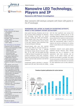
1. Asian giants Samsung, Panasonic and LG are
the top three patent assignees for Nanowire
LED technology. Facing them are several
which between them have raised more than
strong technological challenges.
American Chemical Soc., 122, 1, 188-189)
in 2002 by Postech Foundation for an axial PN
junction architecture. Since then, companies
have shown growing interest in nanowire-based
LED for improved light extraction and thermal
conduction.
Fundamental patents describing a nanowire-
Postech Foundation, Solidlite and LG. In the
mid-2000s, Philips, Nanosys, LG and Seoul Opto
LED patents. Current patented technologies
material and junction architecture to achieve
limited crystal defects and increased luminous
KnowMade’s research covers global patents
published through February 2014. Patents
addressing the use of nanowires in LED
applications have been selected, and an
analysis of the patent holders and their
patented technologies is provided. This report
focuses exclusively on LED and does not include
patents related to the fabrication of nanowires
for other applications such as solar, detectors,
or laser.
Nanowire LED Technology,
Players and IP
Nanowire LED Patent Investigation
NANOWIRE LED: AFTER 10 YEARS OF PATENTING ACTIVITY,
WHAT’S THE CURRENT PATENT SITUATION?
Patent Analysis
Investigation
- Deposition method
- Substrate type
- Active material type
- PN junction type
- Passive material type
technology segments
IP
patents nearing expiration
patents, patented technologies,
partnerships, and patents
nearing expiration
patents analyzed in this report,
and a technology segmentation
data and forecasts
and their roadmap
RELATED REPORTS
Electronics
Investigation
Find all our reports
on www.i-micronews.com
Timeline of patent publications for active devices
(KnowMade, May 2014)
New nanowire LED startups compete with Asian LED giants in
the IP landscape
KnowMade
2 2
5
11
21
29
32
20
32
46
42
4
0
5
10
15
20
25
30
35
40
45
50
2003 2004 2005 2006 2007 2008 2009 2010 2011 2012 2013 2014
No.ofPatentFamilies
Solidlite
TWI220319
LG
Postech Foundation
WO2004114422
Postech
Foundation
KR100462468
2. Nanowire LED Patent Investigation
REFINE YOUR PATENT STRATEGY WITH A DEEP PATENT SEGMENTATION AND
A USEFUL PATENT DATABASE
in Nanowire LED IP, and most of the major Nanowire
LED players are slightly different from the major
LED players. Samsung, LG and Panasonic have
strong IP portfolios related to Nanowire LED,
Nanocrystal, Lextar Electronics and others are
strong new entrants to the Nanowire LED IP
landscape.
and current legal status of patents, this report
Nanowire LED patent holders. Through thorough
includes a detailed portfolio summary including
patents, granted patents near expiration, and
partnerships.
Through a search strategy consisting of
automated and manual screenings, we have been
report, these families are manually segmented
only LED applications but also other applications
i.e. when the PN junction is comprised on the
enhancement). 246 and 116 patent families are
related to active and passive devices, respectively.
The dataset is also organized into various
method, substrate type, active material, passive
material and PN junction architecture. III-N
and ZnO represent the biggest part of patents
architecture, but recently they have started turning toward radial PN junction.
status, citations analysis and impact on Nanowire LED technology.
Our report also includes an Excel database containing all of the analyzed patents. This database allows
priority date, title, abstract, patent assignees, technological segments and legal status for each member
of the patent family.
IDENTIFY KEY PLAYERS AND DISCOVER NEW IP ENTRANTS (I.E. HON
HAI PRECISION INDUSTRY)
Technology segmentation for patents related to active devices
Active devices
Deposition
method
Active
material material
Substrate
PN Junction Type
Mechanisms :
VLS, SLS
Methods :
CVD, MBE, HVPE, PVD,
Other Techniques, Not
Specified
osition Acctive SubstrateSubstr
nism III-N
ZnO
GaAs
III-P
Other Materials
Not Specified
Silicon
Sapphire
SiC
III-N
Glass
ZnO
GaAs
Metal
Spinel
Germanium
III-P
Ceramic
Others
Not Specified
Axial
Radial/Core-Shell
Axial & Radial
Not Specified
(KnowMade & Yole Développement, May 2014)
Partnerships between startups and institutions
(KnowMade & Yole Développement, May 2014)
3. Patent Analysis
Korea Institute etc.).
OBJECTIVES OF THE REPORT
> Segmentation by relevance
> Timeline of patent publications
> Timeline by country of publication
> Current legal status of patents
> Timeline of patent assignees
> Country of publication for patent assignees
> Granted patents nearing expiration
> Summary of assignee’s patent portfolios
> Mapping of current IP holders
> Impact of patent portfolios
> Technology segmentation
> Deposition method
> Substrate
> Active material
> PN junction
- Timeline of patent publication
- Key patent families
> Passive devices 65
> Segmentation by relevance
> Timeline of patent publications
> Timeline by country of publication
> Current legal status of patents
> Timeline of patent assignees
> Country of publication for patent assignees
> Granted patents nearing expiration
> Summary of assignee’s patent portfolios
> Impact of patent portfolios
> Mapping of current IP holders
> Technology segmentation
> Passive material
Includes patenting activity for active and
patents, granted patents near expiration, and
partnerships.
> Samsung
> Panasonic
> LG
> CEA
> Seoul Opto Devices
89
> LED industry history
> GaN deposition reactor capacity vs. demand
> Drivers for adoption of LED for general
> Cost structure of lighting products - Analysis
> Overview of LED Front-End
> Focus on GaN-on-Si LEDs
> Focus on Nanowire LEDs
> Overview
> Partnerships
Conclusions 133
Licensable technologies 137
TABLE OF CONTENTS
COMPANIES CITED IN THE REPORT (non-exhaustive list)
-
-
-
AUTHORS
Dr. Audrey Bastard
and Nanotechnology. She holds a PhD
in Physics from the National Polytechnic
Institute of Grenoble, France in
collaboration with STMicroelectronics,
CEA-Leti and CEMES Toulouse. She also
holds a Materials Engineering Degree
from the Superior Engineering School of
Luminy, Marseille, France.
Dr. Hong Lin
Développement as a technology
She is specialized in compound
semiconductors and provides technical
She was in charge of the development
nanotechnologies. She holds a Ph.D in
Physics and Chemistry of materials.
Dr. Milan Rosina is a Technology
LEDs, compound semiconductors and
in 2002 from the INPG in France and has
experience with prominent research
process development, technology due
and technology roadmap evaluation.
Pars Mukish holds a master degree
Lighting Technologies, Compound
Semiconductors and OLEDs to carry
4. PAYMENT METHODS
Check
To pay your invoice using a check, please mail your check to the
following address:
KnowMade S.A.R.L.
2405 route des Dolines, BP 65
06902 Valbonne Sophia Antipolis
FRANCE
Money Transfer
To pay your invoice using a bank money wire transfer please
contact your bank to complete this process. Here is the
information that you will need to submit the payment:
Payee: KnowMade S.A.R.L.
Bank: Banque populaire St Laurent du Var CAP 3000 - Quartier
du lac- 06700 St Laurent du Var
IBAN: FR76 1560 7000 6360 6214 5695 126
BIC/SWIFT: CCBPFRPPNCE
Paypal
In order to pay your invoice via PAYPAL, you must first register at
www.paypal.com. Then you can send money to the KnowMade
S.A.R.L. by entering our E-mail address contact@knowmade.fr as
the recipient and entering the invoice amount.
RETURN ORDER BY
E-mail: contact@knowmade.fr
Mail: KnowMade S.A.R.L. 2405 route des Dolines, BP 65 06902
Sophia Antipolis FRANCE
CONTACT
E-mail: contact@knowmade.fr
I hereby accept KnowMade’s Terms and Conditions of Sale
Signature:
PRODUCT ORDER
⃝ Single user license EURO 3,990
⃝ Corporate license EURO 5,990
For price in dollars, please use the day’s exchange rate. For
French customer, add 20% for VAT.
All reports are delivered electronically in pdf format
*One user license means only one person at the company
can use the report. Please be aware that our publication
will be watermarked on each page with the name of the
recipient and of the organization (the name mentioned on
the PO). This watermark will also mention that the report
sharing is not allowed.
SHIP TO
Name (Mr/Ms/Dr/Pr):
______________________________________
Job Title:
______________________________________
Company:
______________________________________
Address:
______________________________________
City:
______________________________________
State:
______________________________________
Postcode/Zip:
______________________________________
Country:
______________________________________
VAT ID Number for EU members:
______________________________________
Tel:
______________________________________
Email:
______________________________________
Date:
______________________________________
ORDER FORM
Nanowire LED Patent Investigation
May 2014
5. Definitions
“Acceptance”: Action by which the Buyer accepts the terms and conditions of sale in their entirety. It is done by signing the purchase order which
mentions “I hereby accept Knowmade’s Terms and Conditions of Sale”.
“Buyer”: Any business user (i.e. any person acting in the course of its business activities, for its business needs) entering into the following general
conditions to the exclusion of consumers acting in their personal interests.
“Contracting Parties” or “Parties”: The Seller on the one hand and the Buyer on the other hand.
“Intellectual Property Rights” (“IPR”) means any rights held by the Seller in its Products, including any patents, trademarks, registered models, designs,
copyrights, inventions, commercial secrets and know-how, technical information, company or trading names and any other intellectual property rights
or similar in any part of the world, notwithstanding the fact that they have been registered or not and including any pending registration of one of the
above mentioned rights.
“License”: For the reports and databases, 2 different licenses are proposed. The buyer has to choose one license:
1. Single user license: a single individual at the company can use the report.
2. Corporate license: the report can be used by unlimited users within the company. Subsidiaries are not included.
“Products”: Reports are established in PowerPoint and delivered on a PDF format and the database may include Excel files.
“Seller”: Based in Sophia Antipolis (France headquarters), Knowmade is a technology intelligence company specialized in the research and analysis of
scientific and technical information. We provide patent landscapes and scientific state of the art with high added value to businesses and research
laboratories. Our intelligence digests play a key role to define your innovation and development strategy.
1. Scope
1.1 The Contracting Parties undertake to observe the following general conditions when agreed by the Buyer and the Seller. ANY ADDITIONAL,
DIFFERENT, OR CONFLICTING TERMS AND CONDITIONS IN ANY OTHER DOCUMENTS ISSUED BY THE BUYER AT ANY TIME ARE HEREBY OBJECTED TO BY
THE SELLER, SHALL BE WHOLLY INAPPLICABLE TO ANY SALE MADE HEREUNDER AND SHALL NOT BE BINDING IN ANY WAY ON THE SELLER.
1.2 This agreement becomes valid and enforceable between the Contracting Parties after clear and non-equivocal consent by any duly authorized
person representing the Buyer. For these purposes, the Buyer accepts these conditions of sales when signing the purchase order which mentions “I
hereby accept Knowmade’s Terms and Conditions of Sale”. This results in acceptance by the Buyer.
1.3 Orders are deemed to be accepted only upon written acceptance and confirmation by the Seller, within [7 days] from the date of order, to be sent
either by email or to the Buyer’s address. In the absence of any confirmation in writing, orders shall be deemed to have been accepted.
2. Mailing of the Products
2.1 Products are sent by email to the Buyer:
- within [1] month from the order for Products already released; or
- within a reasonable time for Products ordered prior to their effective release. In this case, the Seller shall use its best endeavours to inform the Buyer
of an indicative release date and the evolution of the work in progress.
2.2 Some weeks prior to the release date the Seller can propose a pre-release discount to the Buyer.
The Seller shall by no means be responsible for any delay in respect of article 2.2 above, and including in cases where a new event or access to new
contradictory information would require for the analyst extra time to compute or compare the data in order to enable the Seller to deliver a high
quality Products.
2.3 The mailing of the Product will occur only upon payment by the Buyer, in accordance with the conditions contained in article 3.
2.4 The mailing is operated through electronic means either by email via the sales department. If the Product’s electronic delivery format is defective,
the Seller undertakes to replace it at no charge to the Buyer provided that it is informed of the defective formatting within 90 days from the date of
the original download or receipt of the Product.
2.5 The person receiving the Products on behalf of the Buyer shall immediately verify the quality of the Products and their conformity to the order.
Any claim for apparent defects or for non-conformity shall be sent in writing to the Seller within 8 days of receipt of the Products. For this purpose, the
Buyer agrees to produce sufficient evidence of such defects.
2.6 No return of Products shall be accepted without prior information to the Seller, even in case of delayed delivery. Any Product returned to the Seller
without providing prior information to the Seller as required under article 2.5 shall remain at the Buyer’s risk.
3. Price, invoicing and payment
3.1 Prices are given in the orders corresponding to each Product sold on a unit basis or corresponding to annual subscriptions. They are expressed to
be inclusive of all taxes. The prices may be reevaluated from time to time. The effective price is deemed to be the one applicable at the time of the
order.
3.2 Payments due by the Buyer shall be sent by cheque payable to Knowmade, PayPal or by electronic transfer to the following account:
Banque populaire St Laurent du Var CAP 3000 - Quartier du lac- 06700 St Laurent du Var
BIC or SWIFT code: CCBPFRPPNCE
IBAN: : FR76 1560 7000 6360 6214 5695 126
To ensure the payments, the Seller reserves the right to request down payments from the Buyer. In this case, the need of down payments will be
mentioned on the order.
3.3 Payment is due by the Buyer to the Seller within 30 days from invoice date, except in the case of a particular written agreement. If the Buyer fails
to pay within this time and fails to contact the Seller, the latter shall be entitled to invoice interest in arrears based on the annual rate Refi of the
«BCE» + 7 points, in accordance with article L. 441-6 of the French Commercial Code. Our publications (report, database, tool...) are delivered only
after reception of the payment.
3.4 In the event of termination of the contract, or of misconduct, during the contract, the Seller will have the right to invoice at the stage in progress,
and to take legal action for damages.
4. Liabilities
4.1 The Buyer or any other individual or legal person acting on its behalf, being a business user buying the Products for its business activities, shall be
solely responsible for choosing the Products and for the use and interpretations he makes of the documents it purchases, of the results he obtains, and
of the advice and acts it deduces thereof.
TERMS AND CONDITIONS OF SALES
6. 4.2 The Seller shall only be liable for (i) direct and (ii) foreseeable pecuniary loss, caused by the Products or arising from a material breach of this
agreement
4.3 In no event shall the Seller be liable for:
a) damages of any kind, including without limitation, incidental or consequential damages (including, but not limited to, damages for loss of profits,
business interruption and loss of programs or information) arising out of the use of or inability to use the Seller’s website or the Products, or any
information provided on the website, or in the Products;
b) any claim attributable to errors, omissions or other inaccuracies in the Product or interpretations thereof.
4.4 All the information contained in the Products has been obtained from sources believed to be reliable. The Seller does not warrant the accuracy,
completeness adequacy or reliability of such information, which cannot be guaranteed to be free from errors.
4.5 All the Products that the Seller sells may, upon prior notice to the Buyer from time to time be modified by or substituted with similar Products
meeting the needs of the Buyer. This modification shall not lead to the liability of the Seller, provided that the Seller ensures the substituted Product is
similar to the Product initially ordered.
4.6 In the case where, after inspection, it is acknowledged that the Products contain defects, the Seller undertakes to replace the defective products as
far as the supplies allow and without indemnities or compensation of any kind for labor costs, delays, loss caused or any other reason. The
replacement is guaranteed for a maximum of two months starting from the delivery date. Any replacement is excluded for any event as set out in
article 5 below.
4.7 The deadlines that the Seller is asked to state for the mailing of the Products are given for information only and are not guaranteed. If such
deadlines are not met, it shall not lead to any damages or cancellation of the orders, except for non-acceptable delays exceeding [4] months from the
stated deadline, without information from the Seller. In such case only, the Buyer shall be entitled to ask for a reimbursement of its first down
payment to the exclusion of any further damages.
4.8 The Seller does not make any warranties, express or implied, including, without limitation, those of saleability and fitness for a particular purpose,
with respect to the Products. Although the Seller shall take reasonable steps to screen Products for infection of viruses, worms, Trojan horses or other
codes containing contaminating or destructive properties before making the Products available, the Seller cannot guarantee that any Product will be
free from infection.
5. Force majeure
The Seller shall not be liable for any delay in performance directly or indirectly caused by or resulting from acts of nature, fire, flood, accident, riot,
war, government intervention, embargoes, strikes, labor difficulties, equipment failure, late deliveries by suppliers or other difficulties which are
beyond the control, and not the fault of the Seller.
6. Protection of the Seller’s IPR
6.1 All the IPR attached to the Products are and remain the property of the Seller and are protected under French and international copyright law and
conventions.
6.2 The Buyer agreed not to disclose, copy, reproduce, redistribute, resell or publish the Product, or any part of it to any other party other than
employees of its company. The Buyer shall have the right to use the Products solely for its own internal information purposes. In particular, the Buyer
shall therefore not use the Product for purposes such as:
- Information storage and retrieval systems;
- Recordings and re-transmittals over any network (including any local area network);
- use in any timesharing, service bureau, bulletin board or similar arrangement or public display;
- Posting any Product to any other online service (including bulletin boards or the Internet);
- Licensing, leasing, selling, offering for sale or assigning the Product.
6.3 The Buyer shall be solely responsible towards the Seller of all infringements of this obligation, whether this infringement comes from its employees
or any person to whom the Buyer has sent the Products and shall personally take care of any related proceedings, and the Buyer shall bear related
financial consequences in their entirety.
6.4 The Buyer shall define within its company point of contact for the needs of the contract. This person will be the recipient of each new report in PDF
format. This person shall also be responsible for respect of the copyrights and will guaranty that the Products are not disseminated out of the
company.
7. Termination
7.1 If the Buyer cancels the order in whole or in part or postpones the date of mailing, the Buyer shall indemnify the Seller for the entire costs that
have been incurred as at the date of notification by the Buyer of such delay or cancellation. This may also apply for any other direct or indirect
consequential loss that may be borne by the Seller, following this decision.
7.2 In the event of breach by one Party under these conditions or the order, the non-breaching Party may send a notification to the other by recorded
delivery letter upon which, after a period of thirty (30) days without solving the problem, the non-breaching Party shall be entitled to terminate all the
pending orders, without being liable for any compensation.
8. Miscellaneous
All the provisions of these Terms and Conditions are for the benefit of the Seller itself, but also for its licensors, employees and agents. Each of them is
entitled to assert and enforce those provisions against the Buyer.
Any notices under these Terms and Conditions shall be given in writing. They shall be effective upon receipt by the other Party.
The Seller may, from time to time, update these Terms and Conditions and the Buyer, is deemed to have accepted the latest version of these terms
and conditions, provided they have been communicated to him in due time.
9. Governing law and jurisdiction
9.1 Any dispute arising out or linked to these Terms and Conditions or to any contract (orders) entered into in application of these Terms and
Conditions shall be settled by the French Commercial Courts of Grasse, which shall have exclusive jurisdiction upon such issues.
9.2 French law shall govern the relation between the Buyer and the Seller, in accordance with these Terms and Conditions.