Electron microscopy
Lightmicroscopes cannot resolve structures closer than
200 nm because shortest wavelength of visible light is
400 nm
Electrons have wavelengths of 0.01 nm to 0.001 nm, so
electron microscopes have greater resolving power and
greater magnification
Magnify objects 10,000X to 100,000X
Provide detailed views of bacteria, viruses, internal
cellular structures, molecules, and large atoms
2.
Electron microscopy
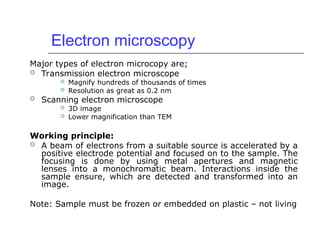
Major typesof electron microcopy are;
Transmission electron microscope
Magnify hundreds of thousands of times
Resolution as great as 0.2 nm
Scanning electron microscope
3D image
Lower magnification than TEM
Working principle:
A beam of electrons from a suitable source is accelerated by a
positive electrode potential and focused on to the sample. The
focusing is done by using metal apertures and magnetic
lenses into a monochromatic beam. Interactions inside the
sample ensure, which are detected and transformed into an
image.
Note: Sample must be frozen or embedded on plastic – not living
3.
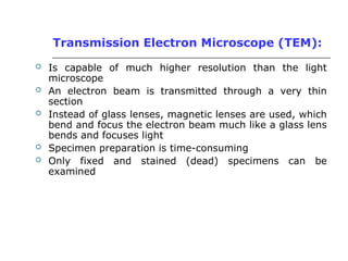
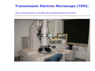
Transmission Electron Microscope(TEM):
Is capable of much higher resolution than the light
microscope
An electron beam is transmitted through a very thin
section
Instead of glass lenses, magnetic lenses are used, which
bend and focus the electron beam much like a glass lens
bends and focuses light
Specimen preparation is time-consuming
Only fixed and stained (dead) specimens can be
examined
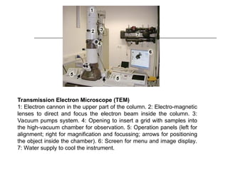
Transmission Electron Microscope(TEM)
1: Electron cannon in the upper part of the column. 2: Electro-magnetic
lenses to direct and focus the electron beam inside the column. 3:
Vacuum pumps system. 4: Opening to insert a grid with samples into
the high-vacuum chamber for observation. 5: Operation panels (left for
alignment; right for magnification and focussing; arrows for positioning
the object inside the chamber). 6: Screen for menu and image display.
7: Water supply to cool the instrument.
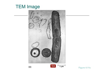
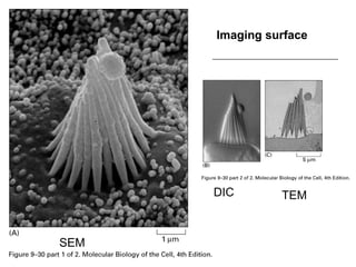
TEM Image: (thinsection of Myrionecta rubra) (Hansen &
Fenchel, Mar. Biol. Res., 2: 169-177, 2006)
9.
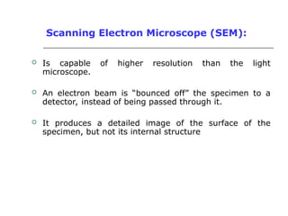
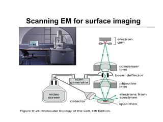
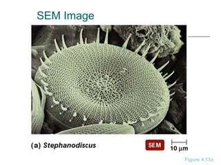
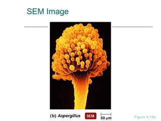
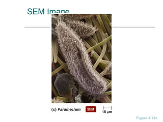
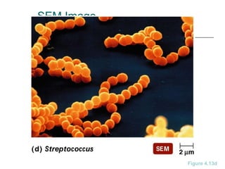
Scanning Electron Microscope(SEM):
Is capable of higher resolution than the light
microscope.
An electron beam is “bounced off” the specimen to a
detector, instead of being passed through it.
It produces a detailed image of the surface of the
specimen, but not its internal structure
10.
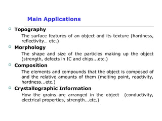
Main Applications
Topography
Thesurface features of an object and its texture (hardness,
reflectivity… etc.)
Morphology
The shape and size of the particles making up the object
(strength, defects in IC and chips...etc.)
Composition
The elements and compounds that the object is composed of
and the relative amounts of them (melting point, reactivity,
hardness...etc.)
Crystallographic Information
How the grains are arranged in the object (conductivity,
electrical properties, strength...etc.)
11.
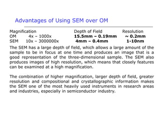
Advantages of UsingSEM over OM
Magnification Depth of Field Resolution
OM 4x – 1000x 15.5mm – 0.19mm ~ 0.2mm
SEM 10x – 3000000x 4mm – 0.4mm 1-10nm
The SEM has a large depth of field, which allows a large amount of the
sample to be in focus at one time and produces an image that is a
good representation of the three-dimensional sample. The SEM also
produces images of high resolution, which means that closely features
can be examined at a high magnification.
The combination of higher magnification, larger depth of field, greater
resolution and compositional and crystallographic information makes
the SEM one of the most heavily used instruments in research areas
and industries, especially in semiconductor industry.
12.
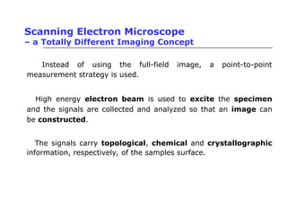
Scanning Electron Microscope
–a Totally Different Imaging Concept
• Instead of using the full-field image, a point-to-point
measurement strategy is used.
• High energy electron beam is used to excite the specimen
and the signals are collected and analyzed so that an image can
be constructed.
• The signals carry topological, chemical and crystallographic
information, respectively, of the samples surface.
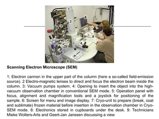
Scanning Electron Microscope(SEM)
1: Electron cannon in the upper part of the column (here a so-called field-emission
source). 2 Electro-magnetic lenses to direct and focus the electron beam inside the
column. 3: Vacuum pumps system. 4: Opening to insert the object into the high-
vacuum observation chamber in conventional SEM mode. 5: Operation panel with
focus, alignment and magnification tools and a joystick for positioning of the
sample. 6: Screen for menu and image display. 7: Cryo-unit to prepare (break, coat
and sublimate) frozen material before insertion in the observation chamber in Cryo-
SEM mode. 8: Electronics stored in cupboards under the desk. 9: Technicians
Mieke Wolters-Arts and Geert-Jan Janssen discussing a view
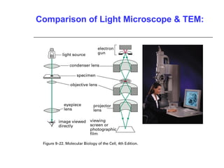
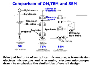
Principal features ofan optical microscope, a transmission
electron microscope and a scanning electron microscope,
drawn to emphasize the similarities of overall design.
Comparison of OM,TEM and SEM
OM TEM SEM
Magnetic
lenses
detector
CRT
Cathode
Ray Tube
Light source
Source of
electrons
Condenser
Specimen
Objective
Eyepiece
Projector Specimen
Editor's Notes
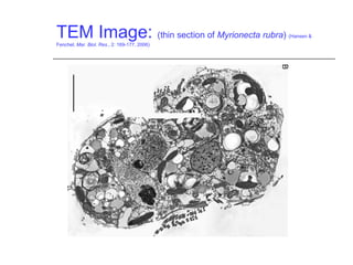
#8 Figure 3. Transmission electron micrograph of a Mesodinium
rubrum cell showing two macronuclei and the symbiont nucleus.
Scale bar = 5 μm.