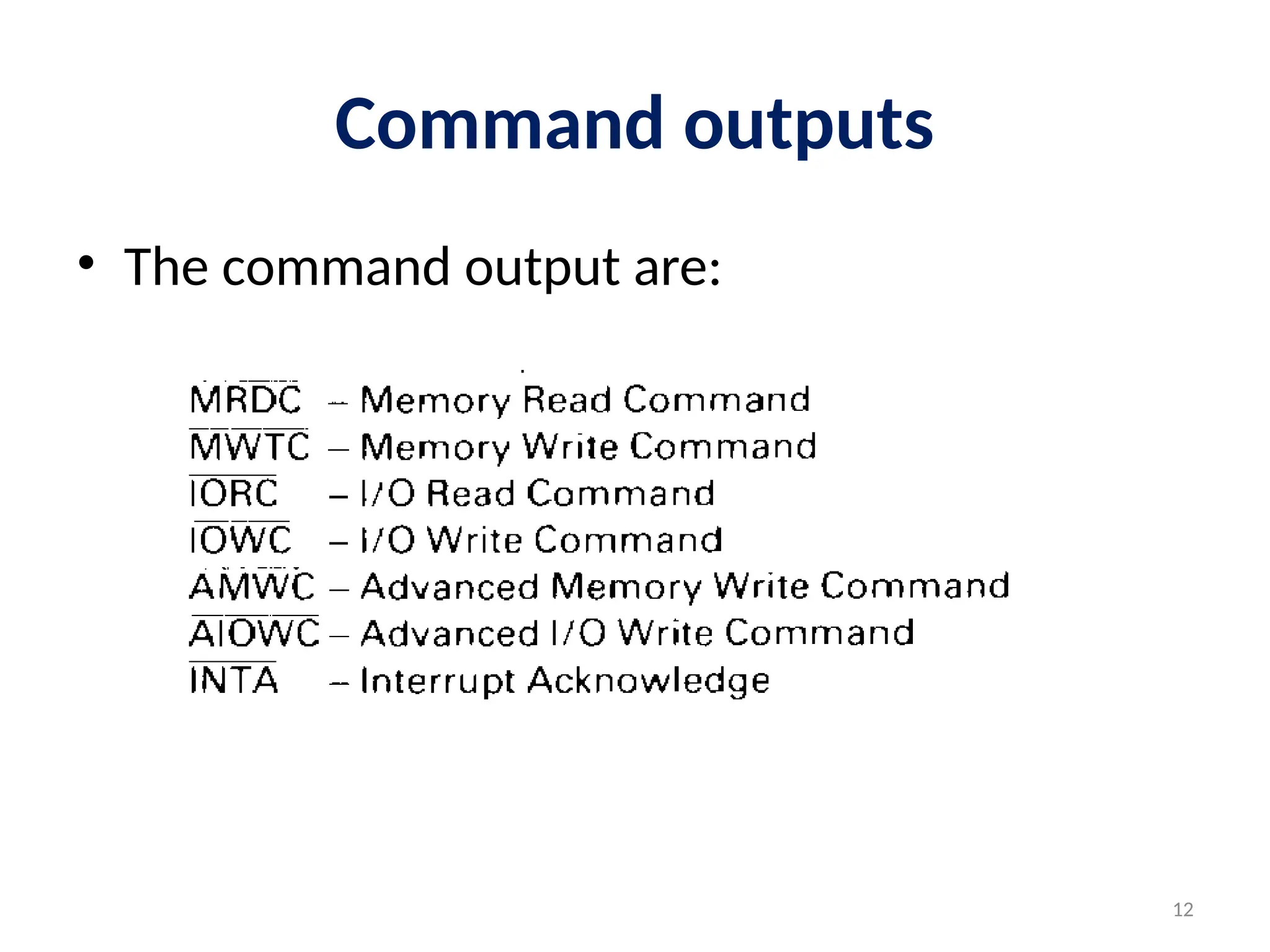
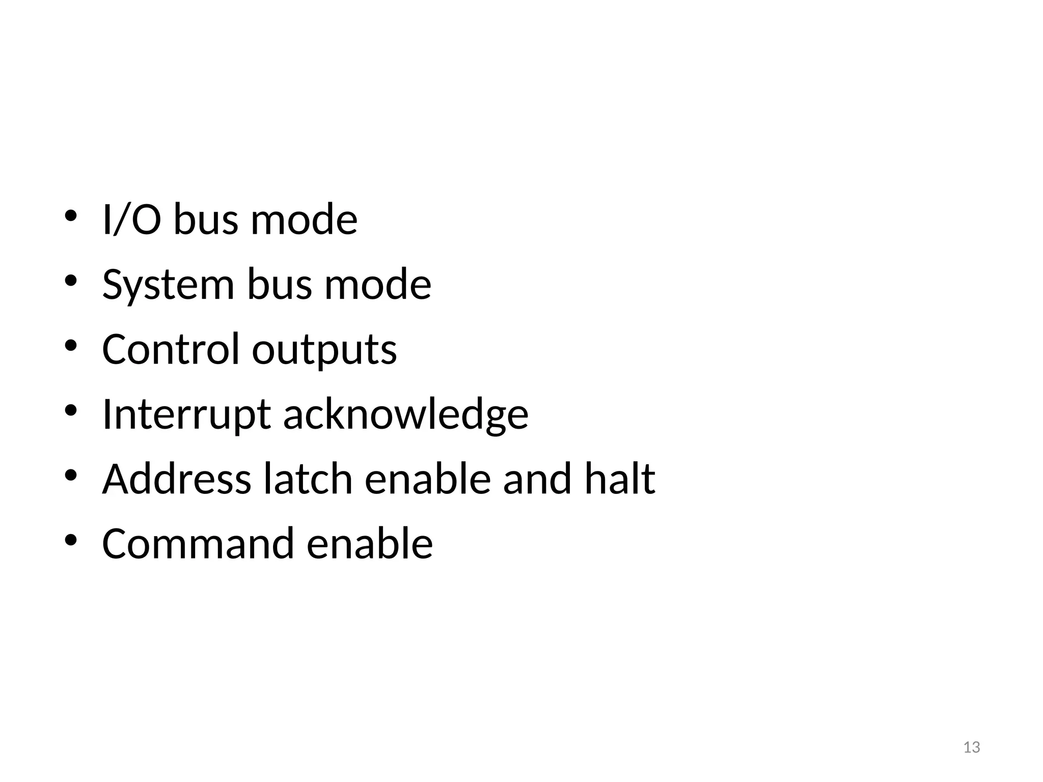
1
8288 Bus Controller
2
8288 Bus controller
• Fully compatible with 8088
• Needs 40% less power supply than standard
8088
• Bipolar drive capability
• Provides advanced commands
3
• Provides wide flexibility in system
configurations
• 3-state command output drivers
• Configurable for use with an I/O bus
• Facilitates interface to one or two multi
master busses
4
5
• 20-pin bipolar
• Command and control timing generations as
well as bipolar bus drive capability
• Multi-master system bus and I/O bus
• Fabricated in a fast bipolar ASBC (Advanced
Standard Buried Collector)
6
7
8
9
10
11
12
Command outputs
• The command output are:
13
• I/O bus mode
• System bus mode
• Control outputs
• Interrupt acknowledge
• Address latch enable and halt
• Command enable
14
15
16
17
18
19
20
21
22
8288 BUS CONTROLLER IN DETAIL
• The 8288 is a 20-pin
chip specially
designed to provide
all the control signals
when the 8088/86 is
in maximum mode.
1
2
3
4
5
6
7
8
9
10
8
2
8
8
20
19
18
17
16
15
14
13
12
11
Vcc
S0
S2
MCE/PDEN
DEN
CEN
INTA
IORC
AIOWC
IOWC
IOB
CLK
S1
DT/R
ALE
AEN
MRDC
AMWC
MWTC
GND
Input signals
S0, S1, S2 (status input)
• Input to these pins comes from
the 8088/86.
• Depending upon the input from
the CPU, the 8288 will provide
one of the commands or control
signals shown in The following
table.
1
2
3
4
5
6
7
8
9
10
8
2
8
8
20
19
18
17
16
15
14
13
12
11
Vcc
S0
S2
MCE/PDEN
DEN
CEN
INTA
IORC
AIOWC
IOWC
IOB
CLK
S1
DT/R
ALE
AEN
MRDC
AMWC
MWTC
GND
CLK (clock)
• This is input from the 8284 clock
generator, providing the clock
pulse to the 8288 to synchronize
all command and control signals
with the CPU.
1
2
3
4
5
6
7
8
9
10
8
2
8
8
20
19
18
17
16
15
14
13
12
11
Vcc
S0
S2
MCE/PDEN
DEN
CEN
INTA
IORC
AIOWC
IOWC
IOB
CLK
S1
DT/R
ALE
AEN
MRDC
AMWC
MWTC
GND
AEN (address enable)
• AEN, an active-low signal,
activates the 8288 command
output at least 115 ns after its
activation.
• In the IBM PC it is connected to
the AEN generation circuitry.
1
2
3
4
5
6
7
8
9
10
8
2
8
8
20
19
18
17
16
15
14
13
12
11
Vcc
S0
S2
MCE/PDEN
DEN
CEN
INTA
IORC
AIOWC
IOWC
IOB
CLK
S1
DT/R
ALE
AEN
MRDC
AMWC
MWTC
GND
CEN (command enable)
• An active-high signal is used to
activate/enable the command
signals and DEN.
• In the IBM PC it is connected to
the AEN generating circuitry
1
2
3
4
5
6
7
8
9
10
8
2
8
8
20
19
18
17
16
15
14
13
12
11
Vcc
S0
S2
MCE/PDEN
DEN
CEN
INTA
IORC
AIOWC
IOWC
IOB
CLK
S1
DT/R
ALE
AEN
MRDC
AMWC
MWTC
GND
IOB
(input/output bus mode)
• An active-high signal makes the
8288 operate in input/output bus
mode rather than in system bus
mode.
• Since the IBM PC is designed with
system buses, it is connected to
low.
1
2
3
4
5
6
7
8
9
10
8
2
8
8
20
19
18
17
16
15
14
13
12
11
Vcc
S0
S2
MCE/PDEN
DEN
CEN
INTA
IORC
AIOWC
IOWC
IOB
CLK
S1
DT/R
ALE
AEN
MRDC
AMWC
MWTC
GND
Output signals
MRDC
(memory read command)
• This is active low and provides
the MEMR (memory read) control
signal.
• It activates the selected device or
memory to release its data to the
data bus.
1
2
3
4
5
6
7
8
9
10
8
2
8
8
20
19
18
17
16
15
14
13
12
11
Vcc
S0
S2
MCE/PDEN
DEN
CEN
INTA
IORC
AIOWC
IOWC
IOB
CLK
S1
DT/R
ALE
AEN
MRDC
AMWC
MWTC
GND
• MWTC
(memory write command),
• AMWC
(advanced memory write)
• These two active-low signals
• used to tell memory to record the data
present on the data bus.
• These two are the same as the MEMW
(memory write) signal,
• the only difference being that AMWT is
activated slightly earlier in order to give
extra time to slow devices.
• In the IBM PC, only MWTC is used as the
MEMW (memory write) control signal,
and AMWC is unused.
1
2
3
4
5
6
7
8
9
10
8
2
8
8
20
19
18
17
16
15
14
13
12
11
Vcc
S0
S2
MCE/PDEN
DEN
CEN
INTA
IORC
AIOWC
IOWC
IOB
CLK
S1
DT/R
ALE
AEN
MRDC
AMWC
MWTC
GND
IORC
(I/O read command)
• IORC is an active-low signal
• tells the I/O device to release its
data into the data bus.
• In the PC it is called the IOR (I/O
read) control signal.
1
2
3
4
5
6
7
8
9
10
8
2
8
8
20
19
18
17
16
15
14
13
12
11
Vcc
S0
S2
MCE/PDEN
DEN
CEN
INTA
IORC
AIOWC
IOWC
IOB
CLK
S1
DT/R
ALE
AEN
MRDC
AMWC
MWTC
GND
• IOWC
(I/O write command)
• AIOWC
(advanced I/O write command)
• Both are active-low signals
• used to tell the I/O device to pick up
the data on the data bus.
• AIOWC is available a little bit early to
give sufficient time to slow devices.
• It is unused in the IBM PC. In the PC,
• IOWC is labeled as IOW.
1
2
3
4
5
6
7
8
9
10
8
2
8
8
20
19
18
17
16
15
14
13
12
11
Vcc
S0
S2
MCE/PDEN
DEN
CEN
INTA
IORC
AIOWC
IOWC
IOB
CLK
S1
DT/R
ALE
AEN
MRDC
AMWC
MWTC
GND
INTA
(interrupt acknowledge)
• An active-low signal will inform the
interrupting device that its interrupt
has been acknowledged and will
provide the vector address to the
data bus.
• In the IBM PC this is connected to
INTA of the 8259 interrupt controller
chip.
1
2
3
4
5
6
7
8
9
10
8
2
8
8
20
19
18
17
16
15
14
13
12
11
Vcc
S0
S2
MCE/PDEN
DEN
CEN
INTA
IORC
AIOWC
IOWC
IOB
CLK
S1
DT/R
ALE
AEN
MRDC
AMWC
MWTC
GND
DT/R
(data transmit/receive)
• DT/R is used to control the direction of
data in and out of the 8088/86.
• In the IBM PC it is connected to DIR of the
74LS245.
• When the 8088/86 is writing data, this
signal is high and will allow data to go
from the A side to the B side of the
74LS245, so that data is released to the
system bus.
• Conversely, when the CPU is reading data,
this signal is low, which allows data to
come in from the B to the A side of the
74LS245 data transceiver chip so that it
can be received by the CPU.
1
2
3
4
5
6
7
8
9
10
8
2
8
8
20
19
18
17
16
15
14
13
12
11
Vcc
S0
S2
MCE/PDEN
DEN
CEN
INTA
IORC
AIOWC
IOWC
IOB
CLK
S1
DT/R
ALE
AEN
MRDC
AMWC
MWTC
GND
DEN
(data enable)
• An active-high signal
• will make the data bus either a
local data bus or the system data
bus.
• In the IBM PC it is used along
with a signal from the 8259
interrupt controller to activate G
of the 74LS245 transceiver.
1
2
3
4
5
6
7
8
9
10
8
2
8
8
20
19
18
17
16
15
14
13
12
11
Vcc
S0
S2
MCE/PDEN
DEN
CEN
INTA
IORC
AIOWC
IOWC
IOB
CLK
S1
DT/R
ALE
AEN
MRDC
AMWC
MWTC
GND
MCE/PDEN
(Master cascade enable/peripheral
data enable)
• This is used along with the 8259
interrupt controller in master
configuration. In the IBM PC the
8259 is used as a slave; therefore,
this pin is ignored.
1
2
3
4
5
6
7
8
9
10
8
2
8
8
20
19
18
17
16
15
14
13
12
11
Vcc
S0
S2
MCE/PDEN
DEN
CEN
INTA
IORC
AIOWC
IOWC
IOB
CLK
S1
DT/R
ALE
AEN
MRDC
AMWC
MWTC
GND
ALE
(address latch enable)
• ALE is an active-high signal used to
activate address latches.
• The 8088 multiplexes address and
data through AD0 - AD7 in order to
save pins.
• In the IBM PC, ALE is connected to G
input of the 74LS373, making
demultiplexing of the addresses
possible.
1
2
3
4
5
6
7
8
9
10
8
2
8
8
20
19
18
17
16
15
14
13
12
11
Vcc
S0
S2
MCE/PDEN
DEN
CEN
INTA
IORC
AIOWC
IOWC
IOB
CLK
S1
DT/R
ALE
AEN
MRDC
AMWC
MWTC
GND
Overview of timing
• As shown in Figure , it takes total of 4 clock
pulses for the memory (or I/O) cycle.
• The CPU allows only 4 clocks to read from (or
write to) memory or I/O unless a wait state is
introduced. .
• These 4 clocks are referred to as T1, T2, T3,
and T4.
• In T1, the addresses are put on the address
pins by the CPU and ALE is activated to inform
the demultiplexer to latch them.
• In T2, the control signal MEMR (or IOR for
input) is activated
42
• During T3, the CPU is ready to accept the data
(opcode or operand) read from memory if it is
available
• It is in T4, absolutely at the latest, that the
data must be presented to pins DO - D7 of the
CPU.
IBM PC/XT BUSES
• 8088/86, the 8284A clock generator, and the
8288 bus controller are all connected in the
IBM PC/XT to produce the required buses to
communicate with memory and input/output
peripherals.
45
• There are three buses (besides power and
ground) in the IBM PC:
– the address bus,
– the data bus,
– and the control bus.
• The IBM PC has two masters to access the
buses: 8088 processor and 8237 DMA.
• While the 8088, the main processor, is
designed for fetching and executing
instructions, it is unacceptably slow for
transferring large numbers of bytes of data
such as in hard (or floppy) disk data transfers
47
• The 8237 chip is used for data transfers of
large numbers of bytes
• The 8237's job is to transfer data and it must
have access to all three buses to do that.
• Since no bus can serve two masters at the
same time, there must be a way to allow
either the 8088 processor or the 8237 DMA to
gain control over the buses.
49
• This is called bus arbitration and is achieved by
the AEN (address enable) generation circuitry,
explained below.
• Three 74LS373 chips are used for :
1. To latch the addresses from the 8088 and
provide stable addresses to the entire
computer.
2. The address bus is a unidirectional bus. The
74LS373 chips are activated by control signals
AEN and ALE.
51
• When AEN, which is connected to OE (Output
Enable) is low, the 8088 provides the address
buses to the system.
4. The 8288 provides ALE (connected to G) that
enables the 74LS373 to latch the addresses
from the CPU, providing a 20-line stable
address to all memory, peripherals, and
expansion slots.
53
• Demultiplexing addresses A0 - A7 is
performed by the 74LS373 connected to pins
AD0 - AD7 of the CPU.
• The CPU's A8 - A15 is connected to the second
74LS373 and A16 - A19 to the third one.
• Half of the third 74LS373 is unused.
• To isolate the system address buses from local
address buses.
• It needs to be emphasized that the system
buses must be allowed to be used by the DMA
or any other board through the expansion slot
without disturbing the CPU.
• This is achieved by the 74LS373s through AEN.
Data bus
• The bidirectional data bus goes through the
74LS245 transceiver.
• DT/R and DEN are the two signals that activate
the 74LS245.
56
• DT/R goes to DIR of the 74LS245 and makes
the transceiver transmit information from the
A side to the B side when DT/R is high.
57
• Conversely, when DT/R makes DIR low, the
transceiver transfers information from the B
side to the A side, thereby receiving
information from the system data bus,
bringing it to the microprocessor.
• DEN, along with a high signal from the 8259
interrupt controller (when the interrupt
controller is not activated it provides a high to
SP/EN), goes through a NAND gate and
enables the 74LS245 by putting a low on G.
59
• DEN, along with SP/EN, isolates the data buses
to make them either a local bus or a system
bus.
• When the 74LS245's G is not active, the
system data bus is isolated from the local data
bus.
Control bus
• Some control buses are supplied by the 8288,
others are produced by logic circuitry.
Control buses
• IOR (I/O read),
• IOW (I/O write),
• MEMR (memory read),
• MEMW (memory write)
are the most widely used control buses in the PC.
AEN signal generation
• AEN is the output signal
• Specifies that either the Microprocessor
or DMA can access the busses according
to the following table:
Bus Control AEN
CPU by Buses controlled 0
Buses controlled by DMA 1
Control of buses by the 8088/86 CPU
• The 8088/86 controls the system buses
whenever AEN becomes low. This happens in
the following situations:
1. When the computer is RESET. RESET is an
active-high signal, but after it is inverted, it
provides an active-low signal as required by
CLEAR of the 74LS175.
2. If any of the status signals are low. This
happens in every occasion except when the
CPU is in passive mode. The status signals will
all become high in the T4 state, giving a
chance to the pending request by DMA to
use the buses.
65
• When LOCK is active. If the 8088 is executing
an instruction with the lock prefix, it puts a
low on the lock pin, indicating that the CPU
will not release the system bus until the
current instruction is finished.
66
• if a given instruction does not have the LOCK
prefix, the status of the LOCK pin of the 8088
is high during the execution of that
instruction.
67
4. When HRQDMA (hold request from DMA) is
high and as long as there is no request from the
DMA, the system bus is controlled by the
8088/86.
Control of the bus by DMA
• How does AEN become high, handing control
over system buses to DMA?
Ans.: When DMA receives a request for service it
will notify the CPU that it needs to use the
system buses by putting a LOW on HRQDMA.
69
• This in turn will provide a high on the D3
output of the 74LS175, assuming that the
current memory cycle is finished and that
LOCK is not activated.
70
• In the following clock cycle, HLDA is provided
to the DMA and AEN becomes high, giving
control over the buses to the DMA.
Local bus vs. system bus
• Everything on the left of the 8288 (74LS373s
and 74LS245) represents the local bus and
everything on the right side of those chips is
the system buses.
72
• The system bus not only provides necessary
signals to all the chips (RAM, ROM, and
peripheral chips) on the motherboard, but
also goes to the expansion slot for any plug-in
expansion board.
Bus buffering (boosting)
• Bus buffering is nothing more than boosting
the signals traveling on the buses.
• The most widely used signal buffers in PC
design are 74LS244 and 74LS245.
74
• If the bus is unidirectional (e.g., the address
bus), it uses 74XX244s.
• But if it is bidirectional (for example, the data
bus), the 74XX245 is used to boost its
strength.

Microprocessor and Assembly Language - 9.pptx

  • 1.
  • 2.
    2 8288 Bus controller •Fully compatible with 8088 • Needs 40% less power supply than standard 8088 • Bipolar drive capability • Provides advanced commands
  • 3.
    3 • Provides wideflexibility in system configurations • 3-state command output drivers • Configurable for use with an I/O bus • Facilitates interface to one or two multi master busses
  • 4.
  • 5.
    5 • 20-pin bipolar •Command and control timing generations as well as bipolar bus drive capability • Multi-master system bus and I/O bus • Fabricated in a fast bipolar ASBC (Advanced Standard Buried Collector)
  • 6.
  • 7.
  • 8.
  • 9.
  • 10.
  • 11.
  • 12.
    12 Command outputs • Thecommand output are:
  • 13.
    13 • I/O busmode • System bus mode • Control outputs • Interrupt acknowledge • Address latch enable and halt • Command enable
  • 14.
  • 15.
  • 16.
  • 17.
  • 18.
  • 19.
  • 20.
  • 21.
  • 22.
  • 23.
    8288 BUS CONTROLLERIN DETAIL • The 8288 is a 20-pin chip specially designed to provide all the control signals when the 8088/86 is in maximum mode. 1 2 3 4 5 6 7 8 9 10 8 2 8 8 20 19 18 17 16 15 14 13 12 11 Vcc S0 S2 MCE/PDEN DEN CEN INTA IORC AIOWC IOWC IOB CLK S1 DT/R ALE AEN MRDC AMWC MWTC GND
  • 24.
    Input signals S0, S1,S2 (status input) • Input to these pins comes from the 8088/86. • Depending upon the input from the CPU, the 8288 will provide one of the commands or control signals shown in The following table. 1 2 3 4 5 6 7 8 9 10 8 2 8 8 20 19 18 17 16 15 14 13 12 11 Vcc S0 S2 MCE/PDEN DEN CEN INTA IORC AIOWC IOWC IOB CLK S1 DT/R ALE AEN MRDC AMWC MWTC GND
  • 26.
    CLK (clock) • Thisis input from the 8284 clock generator, providing the clock pulse to the 8288 to synchronize all command and control signals with the CPU. 1 2 3 4 5 6 7 8 9 10 8 2 8 8 20 19 18 17 16 15 14 13 12 11 Vcc S0 S2 MCE/PDEN DEN CEN INTA IORC AIOWC IOWC IOB CLK S1 DT/R ALE AEN MRDC AMWC MWTC GND
  • 27.
    AEN (address enable) •AEN, an active-low signal, activates the 8288 command output at least 115 ns after its activation. • In the IBM PC it is connected to the AEN generation circuitry. 1 2 3 4 5 6 7 8 9 10 8 2 8 8 20 19 18 17 16 15 14 13 12 11 Vcc S0 S2 MCE/PDEN DEN CEN INTA IORC AIOWC IOWC IOB CLK S1 DT/R ALE AEN MRDC AMWC MWTC GND
  • 28.
    CEN (command enable) •An active-high signal is used to activate/enable the command signals and DEN. • In the IBM PC it is connected to the AEN generating circuitry 1 2 3 4 5 6 7 8 9 10 8 2 8 8 20 19 18 17 16 15 14 13 12 11 Vcc S0 S2 MCE/PDEN DEN CEN INTA IORC AIOWC IOWC IOB CLK S1 DT/R ALE AEN MRDC AMWC MWTC GND
  • 29.
    IOB (input/output bus mode) •An active-high signal makes the 8288 operate in input/output bus mode rather than in system bus mode. • Since the IBM PC is designed with system buses, it is connected to low. 1 2 3 4 5 6 7 8 9 10 8 2 8 8 20 19 18 17 16 15 14 13 12 11 Vcc S0 S2 MCE/PDEN DEN CEN INTA IORC AIOWC IOWC IOB CLK S1 DT/R ALE AEN MRDC AMWC MWTC GND
  • 30.
    Output signals MRDC (memory readcommand) • This is active low and provides the MEMR (memory read) control signal. • It activates the selected device or memory to release its data to the data bus. 1 2 3 4 5 6 7 8 9 10 8 2 8 8 20 19 18 17 16 15 14 13 12 11 Vcc S0 S2 MCE/PDEN DEN CEN INTA IORC AIOWC IOWC IOB CLK S1 DT/R ALE AEN MRDC AMWC MWTC GND
  • 31.
    • MWTC (memory writecommand), • AMWC (advanced memory write) • These two active-low signals • used to tell memory to record the data present on the data bus. • These two are the same as the MEMW (memory write) signal, • the only difference being that AMWT is activated slightly earlier in order to give extra time to slow devices. • In the IBM PC, only MWTC is used as the MEMW (memory write) control signal, and AMWC is unused. 1 2 3 4 5 6 7 8 9 10 8 2 8 8 20 19 18 17 16 15 14 13 12 11 Vcc S0 S2 MCE/PDEN DEN CEN INTA IORC AIOWC IOWC IOB CLK S1 DT/R ALE AEN MRDC AMWC MWTC GND
  • 32.
    IORC (I/O read command) •IORC is an active-low signal • tells the I/O device to release its data into the data bus. • In the PC it is called the IOR (I/O read) control signal. 1 2 3 4 5 6 7 8 9 10 8 2 8 8 20 19 18 17 16 15 14 13 12 11 Vcc S0 S2 MCE/PDEN DEN CEN INTA IORC AIOWC IOWC IOB CLK S1 DT/R ALE AEN MRDC AMWC MWTC GND
  • 33.
    • IOWC (I/O writecommand) • AIOWC (advanced I/O write command) • Both are active-low signals • used to tell the I/O device to pick up the data on the data bus. • AIOWC is available a little bit early to give sufficient time to slow devices. • It is unused in the IBM PC. In the PC, • IOWC is labeled as IOW. 1 2 3 4 5 6 7 8 9 10 8 2 8 8 20 19 18 17 16 15 14 13 12 11 Vcc S0 S2 MCE/PDEN DEN CEN INTA IORC AIOWC IOWC IOB CLK S1 DT/R ALE AEN MRDC AMWC MWTC GND
  • 34.
    INTA (interrupt acknowledge) • Anactive-low signal will inform the interrupting device that its interrupt has been acknowledged and will provide the vector address to the data bus. • In the IBM PC this is connected to INTA of the 8259 interrupt controller chip. 1 2 3 4 5 6 7 8 9 10 8 2 8 8 20 19 18 17 16 15 14 13 12 11 Vcc S0 S2 MCE/PDEN DEN CEN INTA IORC AIOWC IOWC IOB CLK S1 DT/R ALE AEN MRDC AMWC MWTC GND
  • 35.
    DT/R (data transmit/receive) • DT/Ris used to control the direction of data in and out of the 8088/86. • In the IBM PC it is connected to DIR of the 74LS245. • When the 8088/86 is writing data, this signal is high and will allow data to go from the A side to the B side of the 74LS245, so that data is released to the system bus. • Conversely, when the CPU is reading data, this signal is low, which allows data to come in from the B to the A side of the 74LS245 data transceiver chip so that it can be received by the CPU. 1 2 3 4 5 6 7 8 9 10 8 2 8 8 20 19 18 17 16 15 14 13 12 11 Vcc S0 S2 MCE/PDEN DEN CEN INTA IORC AIOWC IOWC IOB CLK S1 DT/R ALE AEN MRDC AMWC MWTC GND
  • 36.
    DEN (data enable) • Anactive-high signal • will make the data bus either a local data bus or the system data bus. • In the IBM PC it is used along with a signal from the 8259 interrupt controller to activate G of the 74LS245 transceiver. 1 2 3 4 5 6 7 8 9 10 8 2 8 8 20 19 18 17 16 15 14 13 12 11 Vcc S0 S2 MCE/PDEN DEN CEN INTA IORC AIOWC IOWC IOB CLK S1 DT/R ALE AEN MRDC AMWC MWTC GND
  • 37.
    MCE/PDEN (Master cascade enable/peripheral dataenable) • This is used along with the 8259 interrupt controller in master configuration. In the IBM PC the 8259 is used as a slave; therefore, this pin is ignored. 1 2 3 4 5 6 7 8 9 10 8 2 8 8 20 19 18 17 16 15 14 13 12 11 Vcc S0 S2 MCE/PDEN DEN CEN INTA IORC AIOWC IOWC IOB CLK S1 DT/R ALE AEN MRDC AMWC MWTC GND
  • 38.
    ALE (address latch enable) •ALE is an active-high signal used to activate address latches. • The 8088 multiplexes address and data through AD0 - AD7 in order to save pins. • In the IBM PC, ALE is connected to G input of the 74LS373, making demultiplexing of the addresses possible. 1 2 3 4 5 6 7 8 9 10 8 2 8 8 20 19 18 17 16 15 14 13 12 11 Vcc S0 S2 MCE/PDEN DEN CEN INTA IORC AIOWC IOWC IOB CLK S1 DT/R ALE AEN MRDC AMWC MWTC GND
  • 39.
  • 40.
    • As shownin Figure , it takes total of 4 clock pulses for the memory (or I/O) cycle. • The CPU allows only 4 clocks to read from (or write to) memory or I/O unless a wait state is introduced. . • These 4 clocks are referred to as T1, T2, T3, and T4.
  • 41.
    • In T1,the addresses are put on the address pins by the CPU and ALE is activated to inform the demultiplexer to latch them. • In T2, the control signal MEMR (or IOR for input) is activated
  • 42.
    42 • During T3,the CPU is ready to accept the data (opcode or operand) read from memory if it is available • It is in T4, absolutely at the latest, that the data must be presented to pins DO - D7 of the CPU.
  • 43.
  • 44.
    • 8088/86, the8284A clock generator, and the 8288 bus controller are all connected in the IBM PC/XT to produce the required buses to communicate with memory and input/output peripherals.
  • 45.
    45 • There arethree buses (besides power and ground) in the IBM PC: – the address bus, – the data bus, – and the control bus.
  • 46.
    • The IBMPC has two masters to access the buses: 8088 processor and 8237 DMA. • While the 8088, the main processor, is designed for fetching and executing instructions, it is unacceptably slow for transferring large numbers of bytes of data such as in hard (or floppy) disk data transfers
  • 47.
    47 • The 8237chip is used for data transfers of large numbers of bytes • The 8237's job is to transfer data and it must have access to all three buses to do that.
  • 48.
    • Since nobus can serve two masters at the same time, there must be a way to allow either the 8088 processor or the 8237 DMA to gain control over the buses.
  • 49.
    49 • This iscalled bus arbitration and is achieved by the AEN (address enable) generation circuitry, explained below.
  • 50.
    • Three 74LS373chips are used for : 1. To latch the addresses from the 8088 and provide stable addresses to the entire computer. 2. The address bus is a unidirectional bus. The 74LS373 chips are activated by control signals AEN and ALE.
  • 51.
    51 • When AEN,which is connected to OE (Output Enable) is low, the 8088 provides the address buses to the system.
  • 52.
    4. The 8288provides ALE (connected to G) that enables the 74LS373 to latch the addresses from the CPU, providing a 20-line stable address to all memory, peripherals, and expansion slots.
  • 53.
    53 • Demultiplexing addressesA0 - A7 is performed by the 74LS373 connected to pins AD0 - AD7 of the CPU. • The CPU's A8 - A15 is connected to the second 74LS373 and A16 - A19 to the third one. • Half of the third 74LS373 is unused.
  • 54.
    • To isolatethe system address buses from local address buses. • It needs to be emphasized that the system buses must be allowed to be used by the DMA or any other board through the expansion slot without disturbing the CPU. • This is achieved by the 74LS373s through AEN.
  • 55.
    Data bus • Thebidirectional data bus goes through the 74LS245 transceiver. • DT/R and DEN are the two signals that activate the 74LS245.
  • 56.
    56 • DT/R goesto DIR of the 74LS245 and makes the transceiver transmit information from the A side to the B side when DT/R is high.
  • 57.
    57 • Conversely, whenDT/R makes DIR low, the transceiver transfers information from the B side to the A side, thereby receiving information from the system data bus, bringing it to the microprocessor.
  • 58.
    • DEN, alongwith a high signal from the 8259 interrupt controller (when the interrupt controller is not activated it provides a high to SP/EN), goes through a NAND gate and enables the 74LS245 by putting a low on G.
  • 59.
    59 • DEN, alongwith SP/EN, isolates the data buses to make them either a local bus or a system bus. • When the 74LS245's G is not active, the system data bus is isolated from the local data bus.
  • 60.
    Control bus • Somecontrol buses are supplied by the 8288, others are produced by logic circuitry. Control buses • IOR (I/O read), • IOW (I/O write), • MEMR (memory read), • MEMW (memory write) are the most widely used control buses in the PC.
  • 61.
    AEN signal generation •AEN is the output signal • Specifies that either the Microprocessor or DMA can access the busses according to the following table: Bus Control AEN CPU by Buses controlled 0 Buses controlled by DMA 1
  • 62.
    Control of busesby the 8088/86 CPU
  • 63.
    • The 8088/86controls the system buses whenever AEN becomes low. This happens in the following situations: 1. When the computer is RESET. RESET is an active-high signal, but after it is inverted, it provides an active-low signal as required by CLEAR of the 74LS175.
  • 64.
    2. If anyof the status signals are low. This happens in every occasion except when the CPU is in passive mode. The status signals will all become high in the T4 state, giving a chance to the pending request by DMA to use the buses.
  • 65.
    65 • When LOCKis active. If the 8088 is executing an instruction with the lock prefix, it puts a low on the lock pin, indicating that the CPU will not release the system bus until the current instruction is finished.
  • 66.
    66 • if agiven instruction does not have the LOCK prefix, the status of the LOCK pin of the 8088 is high during the execution of that instruction.
  • 67.
    67 4. When HRQDMA(hold request from DMA) is high and as long as there is no request from the DMA, the system bus is controlled by the 8088/86.
  • 68.
    Control of thebus by DMA • How does AEN become high, handing control over system buses to DMA? Ans.: When DMA receives a request for service it will notify the CPU that it needs to use the system buses by putting a LOW on HRQDMA.
  • 69.
    69 • This inturn will provide a high on the D3 output of the 74LS175, assuming that the current memory cycle is finished and that LOCK is not activated.
  • 70.
    70 • In thefollowing clock cycle, HLDA is provided to the DMA and AEN becomes high, giving control over the buses to the DMA.
  • 71.
    Local bus vs.system bus • Everything on the left of the 8288 (74LS373s and 74LS245) represents the local bus and everything on the right side of those chips is the system buses.
  • 72.
    72 • The systembus not only provides necessary signals to all the chips (RAM, ROM, and peripheral chips) on the motherboard, but also goes to the expansion slot for any plug-in expansion board.
  • 73.
    Bus buffering (boosting) •Bus buffering is nothing more than boosting the signals traveling on the buses. • The most widely used signal buffers in PC design are 74LS244 and 74LS245.
  • 74.
    74 • If thebus is unidirectional (e.g., the address bus), it uses 74XX244s. • But if it is bidirectional (for example, the data bus), the 74XX245 is used to boost its strength.