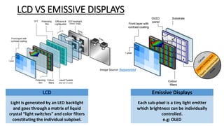
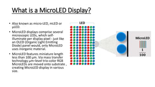
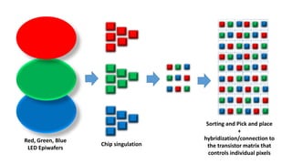
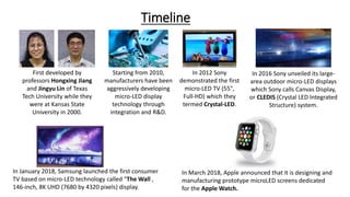
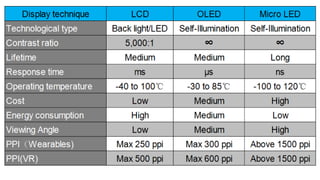
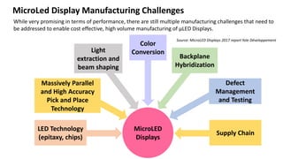
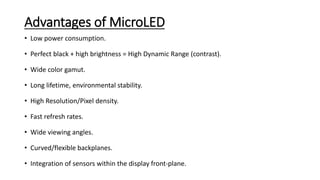
MicroLED
Displays
LCD VS EMISSIVE DISPLAYS
Light is generated by an LED backlight
and goes through a matrix of liquid
crystal “light switches” and color filters
constituting the individual subpixel.
LCD
Each sub-pixel is a tiny light emitter
which brightness can be individually
controlled.
e.g: OLED
Emissive Displays
Image Source: flatpanelshd
What is a MicroLED Display?
• Also known as micro-LED, mLED or
µLED.
• MicroLED displays comprise several
microscopic LEDs, which self-
illuminate per display pixel - just like
an OLED (Organic Light Emitting
Diode) panel would, only MicroLED
uses inorganic material.
• MicroLED features miniature length
less than 100 µm. Via mass transfer
technology µm–level trio-color RGB
MicroLEDs are moved onto substrate ,
creating MicroLED display in various
size.
Red, Green, Blue
LED Epiwafers
Chip singulation
Sorting and Pick and place
+
hybridization/connection to
the transistor matrix that
controls individual pixels
First developed by
professors Hongxing Jiang
and Jingyu Lin of Texas
Tech University while they
were at Kansas State
University in 2000.
Starting from 2010,
manufacturers have been
aggressively developing
micro-LED display
technology through
integration and R&D.
In 2012 Sony
demonstrated the first
micro-LED TV (55",
Full-HD) which they
termed Crystal-LED.
In 2016 Sony unveiled its large-
area outdoor micro-LED displays
which Sony calls Canvas Display,
or CLEDIS (Crystal LED Integrated
Structure) system.
In January 2018, Samsung launched the first consumer
TV based on micro-LED technology called "The Wall ,
146-inch, 8K UHD (7680 by 4320 pixels) display.
In March 2018, Apple announced that it is designing and
manufacturing prototype microLED screens dedicated
for the Apple Watch.
Timeline
TFT-LCD
vs
OLED
vs
MicroLED
MicroLED + Quantum dots
• In a scientific study paper
published by the Optical
Society of America,
MicroLED can also be
combined with quantum
dots (on top, instead of a
passive color filter) to
expand the color space of
the display.
The process flow of the full-color emission of quantum-dot-based micro LED display.
Theory
• Micro-LED displays in theory is making LED structures thinner, smaller, and
in an array structure.
• Individual micro-LEDs usually ranges from 1 to 10 μm, and are transferred
in large volumes onto the IC substrate.
• The substrate can be hard, flexible, transparent or none transparent.
• By using physical vapor deposition to complete a protective layer and
forming the top electrodes it can be packaged into a simple structured
micro LED display.
To Download the PPT and Seminar Report on MicroLED
Visit www.seminarlinks.blogspot.com
Micro-LED structures
• The classical MicroLED structure is a PN junction diode tube made of
direct bandgap semiconductor materials.
• When the MicroLED is forward biased electrons from the
semiconductors conduction band recombine with holes from the
valence band to release photons that emit a monochromatic colored
light.
• In general, MicroLEDs maximum Full Width at Half Maximum (FWHM)
linewdith is 20 nm, and is capable of providing highly color saturation
of more than 120% NTSC.
Manufacturing Methods
• Miniaturization in semiconductor chip processing has reached its
ultimate limit, but there is still great room for growth in miniaturization.
• There are three major production methods for micro-LEDs and can be
categorized into
• Chip Bonding
• Wafer Bonding
• Thin Film Transfer
Chip Bonding
• By splitting LEDs into micro sized Micro LED chips (including Epi-wafer film and
substrate), or using SMT and COB technology, the micro LED chip can be bonded
one-by-one onto the display substrate.
Wafer Bonding
• LED EPI-wafer films will use Inductively Coupled Plasma (ICP) etcher to form a micro
grade micro-LED EPI-wafer film structure, once this structure solidifies it will become
the display pitch.
• Once the LED wafer including the EPI-wafer and substrate are directly bonded to the
IC substrate, manufacturers will use mechanical or chemical processing to strip away
the substrate
• Leaving the 4-5 micron thick micro LED EPI-wafer film structure that construes the
display pixels on the IC driver substrate.
Thin film transfer
• Using the mechanical or chemical method to strip away the LED substrate to
replace it with a temporary LED EPI-wafer to form a micro-LED EPI-wafer
structure.
• Another method is using Inductively Coupled Plasma (ICP) etcher to form
micro-LED EPI-wafer structures, then the substrate is removed using
mechanical or chemical methods, and temporarily replaced with another thin
film.
• Lastly, the display pitch required on the driver IC substrate uses selective
transfer fixture to mass transfer the micro-LED EPI-wafer thin film structures
to bond onto the substrate and form into display pixels.
MicroLED
Displays
LED Technology
(epitaxy, chips)
Supply Chain
Massively Parallel
and High Accuracy
Pick and Place
Technology
Light
extraction and
beam shaping
Color
Conversion
Backplane
Hybridization
Defect
Management
and Testing
While very promising in terms of performance, there are still multiple manufacturing challenges that need to
be addressed to enable cost effective, high volume manufacturing of µLED Displays.
MicroLed Display Manufacturing Challenges
Source: MicroLED Displays 2017 report Yole Développement
Advantages of MicroLED
• Low power consumption.
• Perfect black + high brightness = High Dynamic Range (contrast).
• Wide color gamut.
• Long lifetime, environmental stability.
• High Resolution/Pixel density.
• Fast refresh rates.
• Wide viewing angles.
• Curved/flexible backplanes.
• Integration of sensors within the display front-plane.
Disadvantages of MicroLED
• µLED will remain too expensive & difficult to manufacture for high
volume consumer applications.
• Though this is just a single disadvantage, it branches out to more
problems over time.
• Companies will be reluctant to invest in the expensive facilities and machinery
that are required to make these sorts of panels.
Applications of MicroLED
• Smart Watches and Wearables
• Virtual reality
• Augmented/Mixed Reality
• Automotive Head-Up Display
• Large Video Displays
• 8K UHD TVs
• Smartphones
• Laptop/Tablets
Conclusion
• MicroLED is a promising new display technology with high
performance.
• The biggest companies and startups in technology hardware are
moving forward with the idea.
• There are still multiple manufacturing challenges that need to be
addressed to enable cost effective and high volume manufacturing of
MicroLED Displays.
• MicroLED has the potential to take on and outperform OLED, but it
won’t completely displace OLED and LCD.
• MicroLED Displays 2017 report Yole Développement
• WCCFTECH
• LEDinside
• Pocket-lint
• Cnet
To Download the PPT and Seminar Report on MicroLED
Visit www.seminarlinks.blogspot.com
Thank You

MicroLED.pptx

  • 1.
  • 2.
    LCD VS EMISSIVEDISPLAYS Light is generated by an LED backlight and goes through a matrix of liquid crystal “light switches” and color filters constituting the individual subpixel. LCD Each sub-pixel is a tiny light emitter which brightness can be individually controlled. e.g: OLED Emissive Displays Image Source: flatpanelshd
  • 3.
    What is aMicroLED Display? • Also known as micro-LED, mLED or µLED. • MicroLED displays comprise several microscopic LEDs, which self- illuminate per display pixel - just like an OLED (Organic Light Emitting Diode) panel would, only MicroLED uses inorganic material. • MicroLED features miniature length less than 100 µm. Via mass transfer technology µm–level trio-color RGB MicroLEDs are moved onto substrate , creating MicroLED display in various size.
  • 4.
    Red, Green, Blue LEDEpiwafers Chip singulation Sorting and Pick and place + hybridization/connection to the transistor matrix that controls individual pixels
  • 5.
    First developed by professorsHongxing Jiang and Jingyu Lin of Texas Tech University while they were at Kansas State University in 2000. Starting from 2010, manufacturers have been aggressively developing micro-LED display technology through integration and R&D. In 2012 Sony demonstrated the first micro-LED TV (55", Full-HD) which they termed Crystal-LED. In 2016 Sony unveiled its large- area outdoor micro-LED displays which Sony calls Canvas Display, or CLEDIS (Crystal LED Integrated Structure) system. In January 2018, Samsung launched the first consumer TV based on micro-LED technology called "The Wall , 146-inch, 8K UHD (7680 by 4320 pixels) display. In March 2018, Apple announced that it is designing and manufacturing prototype microLED screens dedicated for the Apple Watch. Timeline
  • 6.
  • 8.
    MicroLED + Quantumdots • In a scientific study paper published by the Optical Society of America, MicroLED can also be combined with quantum dots (on top, instead of a passive color filter) to expand the color space of the display. The process flow of the full-color emission of quantum-dot-based micro LED display.
  • 9.
    Theory • Micro-LED displaysin theory is making LED structures thinner, smaller, and in an array structure. • Individual micro-LEDs usually ranges from 1 to 10 μm, and are transferred in large volumes onto the IC substrate. • The substrate can be hard, flexible, transparent or none transparent. • By using physical vapor deposition to complete a protective layer and forming the top electrodes it can be packaged into a simple structured micro LED display. To Download the PPT and Seminar Report on MicroLED Visit www.seminarlinks.blogspot.com
  • 10.
    Micro-LED structures • Theclassical MicroLED structure is a PN junction diode tube made of direct bandgap semiconductor materials. • When the MicroLED is forward biased electrons from the semiconductors conduction band recombine with holes from the valence band to release photons that emit a monochromatic colored light. • In general, MicroLEDs maximum Full Width at Half Maximum (FWHM) linewdith is 20 nm, and is capable of providing highly color saturation of more than 120% NTSC.
  • 11.
    Manufacturing Methods • Miniaturizationin semiconductor chip processing has reached its ultimate limit, but there is still great room for growth in miniaturization. • There are three major production methods for micro-LEDs and can be categorized into • Chip Bonding • Wafer Bonding • Thin Film Transfer
  • 12.
    Chip Bonding • Bysplitting LEDs into micro sized Micro LED chips (including Epi-wafer film and substrate), or using SMT and COB technology, the micro LED chip can be bonded one-by-one onto the display substrate. Wafer Bonding • LED EPI-wafer films will use Inductively Coupled Plasma (ICP) etcher to form a micro grade micro-LED EPI-wafer film structure, once this structure solidifies it will become the display pitch. • Once the LED wafer including the EPI-wafer and substrate are directly bonded to the IC substrate, manufacturers will use mechanical or chemical processing to strip away the substrate • Leaving the 4-5 micron thick micro LED EPI-wafer film structure that construes the display pixels on the IC driver substrate.
  • 13.
    Thin film transfer •Using the mechanical or chemical method to strip away the LED substrate to replace it with a temporary LED EPI-wafer to form a micro-LED EPI-wafer structure. • Another method is using Inductively Coupled Plasma (ICP) etcher to form micro-LED EPI-wafer structures, then the substrate is removed using mechanical or chemical methods, and temporarily replaced with another thin film. • Lastly, the display pitch required on the driver IC substrate uses selective transfer fixture to mass transfer the micro-LED EPI-wafer thin film structures to bond onto the substrate and form into display pixels.
  • 15.
    MicroLED Displays LED Technology (epitaxy, chips) SupplyChain Massively Parallel and High Accuracy Pick and Place Technology Light extraction and beam shaping Color Conversion Backplane Hybridization Defect Management and Testing While very promising in terms of performance, there are still multiple manufacturing challenges that need to be addressed to enable cost effective, high volume manufacturing of µLED Displays. MicroLed Display Manufacturing Challenges Source: MicroLED Displays 2017 report Yole Développement
  • 16.
    Advantages of MicroLED •Low power consumption. • Perfect black + high brightness = High Dynamic Range (contrast). • Wide color gamut. • Long lifetime, environmental stability. • High Resolution/Pixel density. • Fast refresh rates. • Wide viewing angles. • Curved/flexible backplanes. • Integration of sensors within the display front-plane.
  • 17.
    Disadvantages of MicroLED •µLED will remain too expensive & difficult to manufacture for high volume consumer applications. • Though this is just a single disadvantage, it branches out to more problems over time. • Companies will be reluctant to invest in the expensive facilities and machinery that are required to make these sorts of panels.
  • 18.
    Applications of MicroLED •Smart Watches and Wearables • Virtual reality • Augmented/Mixed Reality • Automotive Head-Up Display • Large Video Displays • 8K UHD TVs • Smartphones • Laptop/Tablets
  • 20.
    Conclusion • MicroLED isa promising new display technology with high performance. • The biggest companies and startups in technology hardware are moving forward with the idea. • There are still multiple manufacturing challenges that need to be addressed to enable cost effective and high volume manufacturing of MicroLED Displays. • MicroLED has the potential to take on and outperform OLED, but it won’t completely displace OLED and LCD.
  • 21.
    • MicroLED Displays2017 report Yole Développement • WCCFTECH • LEDinside • Pocket-lint • Cnet
  • 22.
    To Download thePPT and Seminar Report on MicroLED Visit www.seminarlinks.blogspot.com Thank You