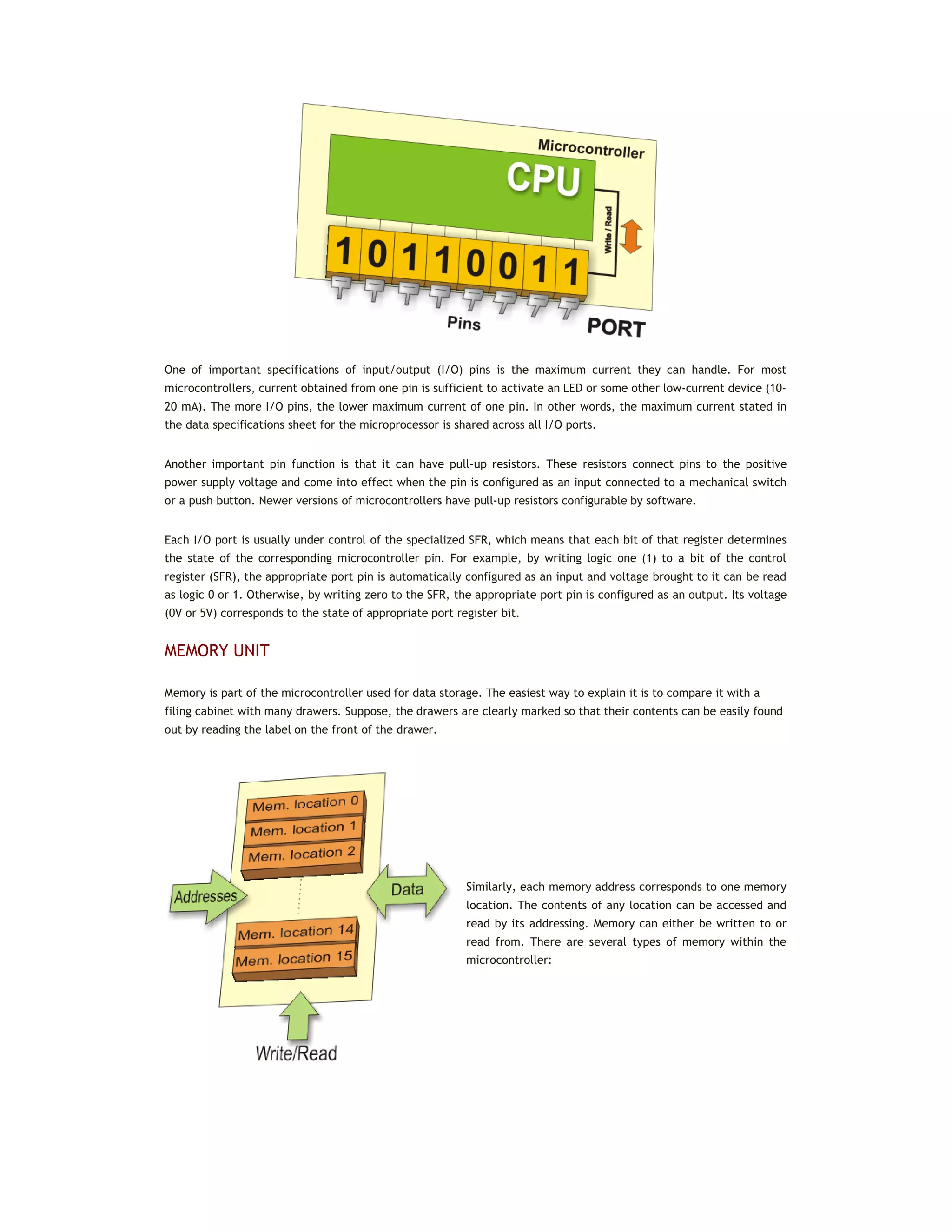
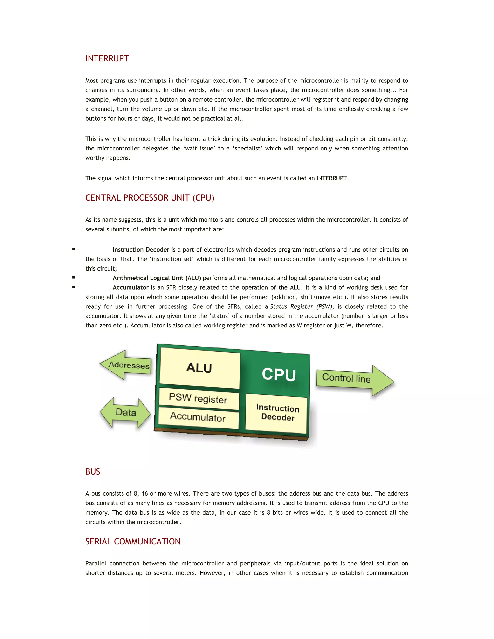
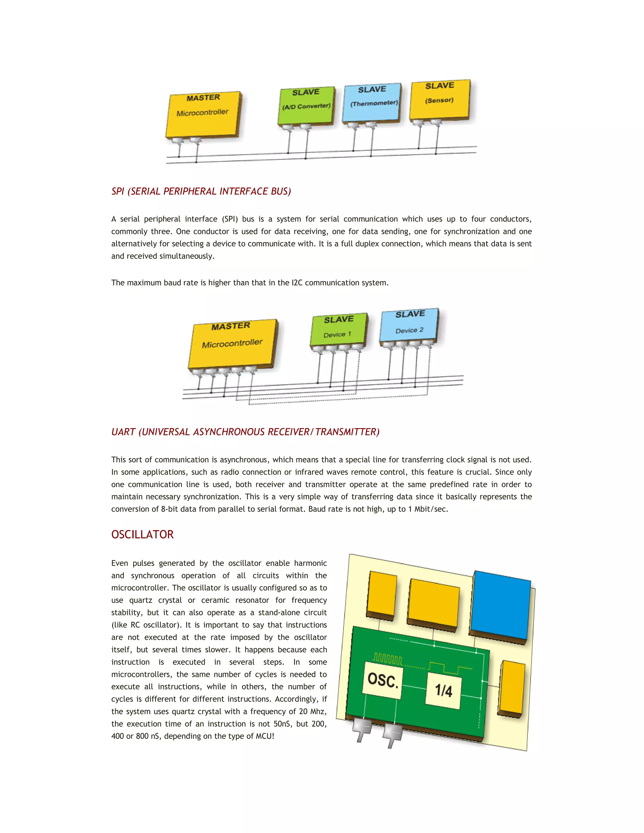
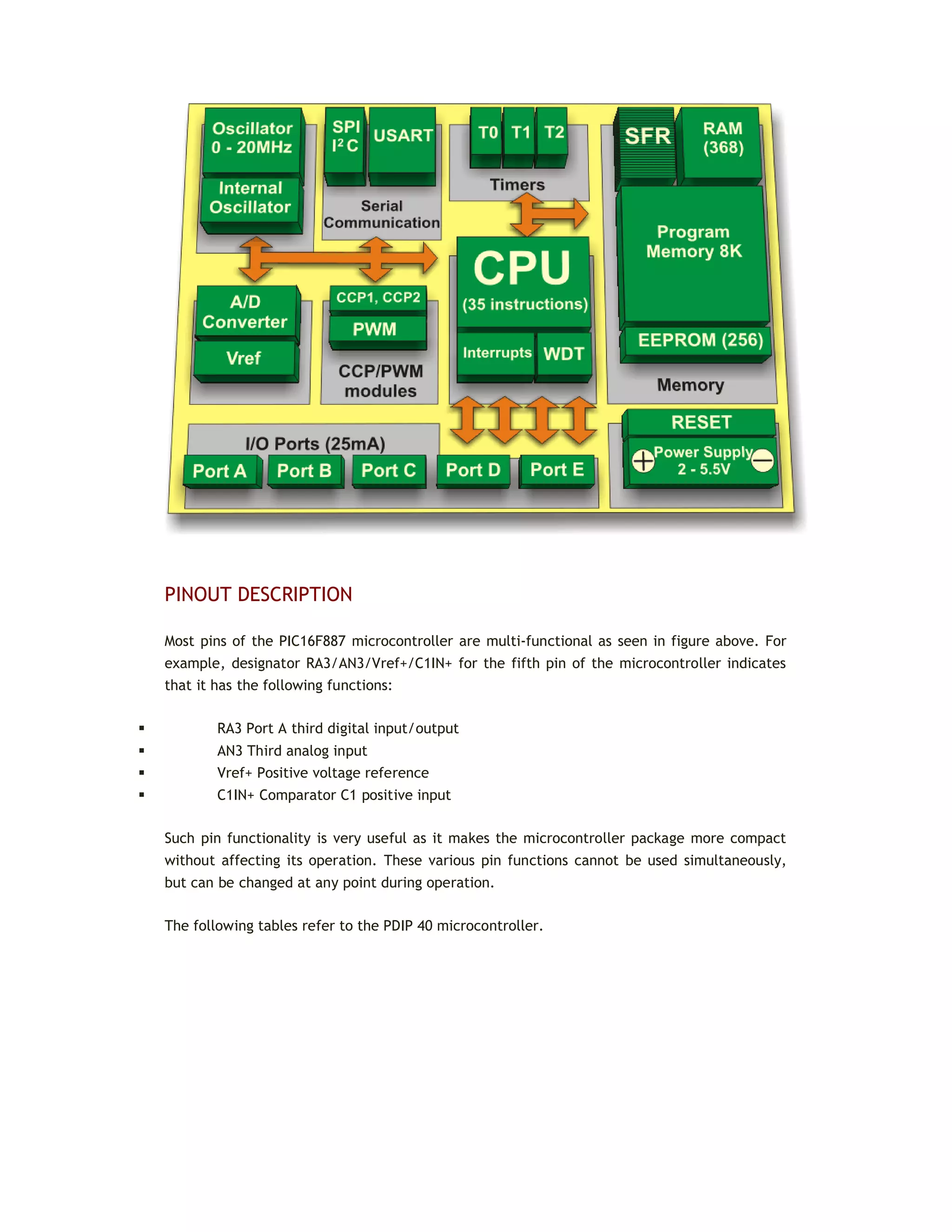
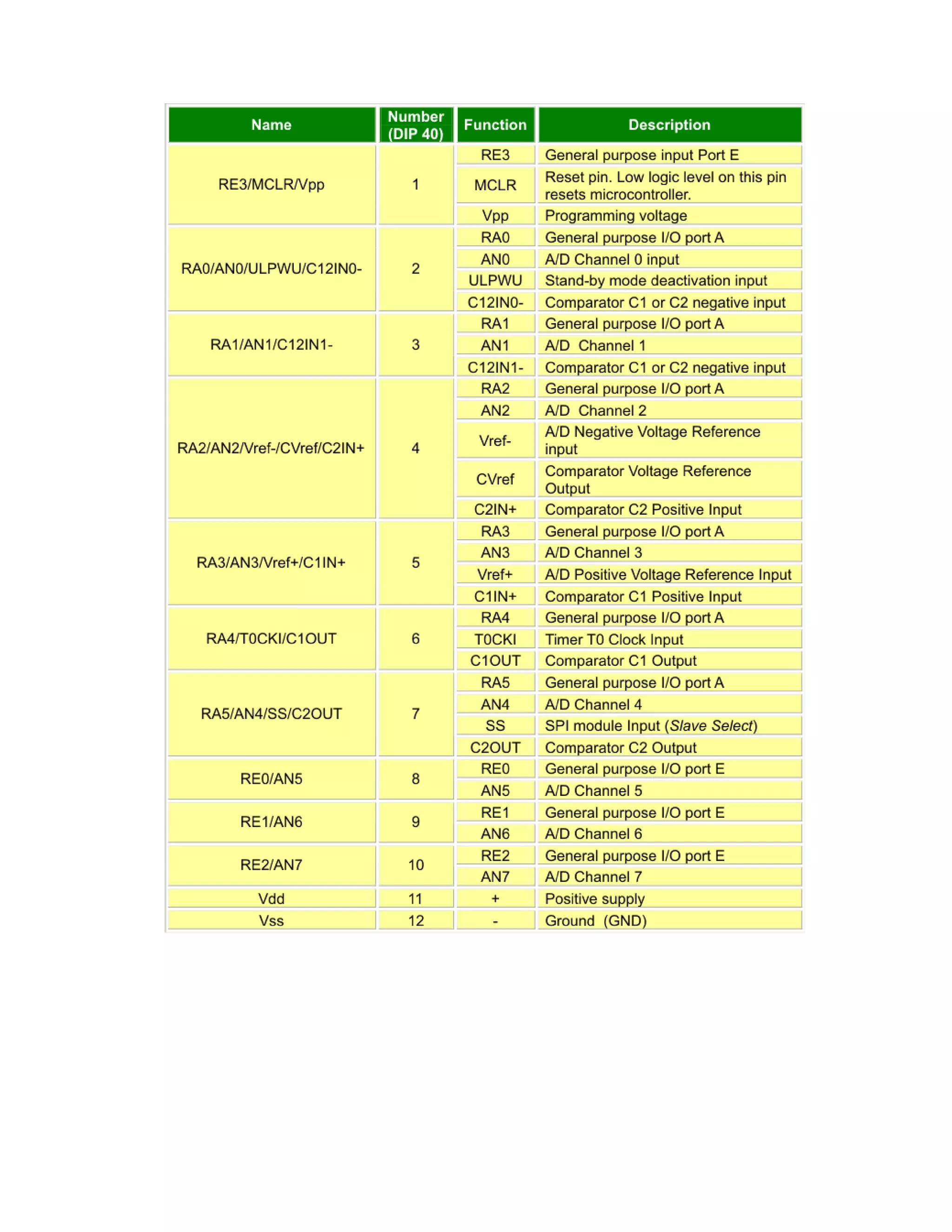
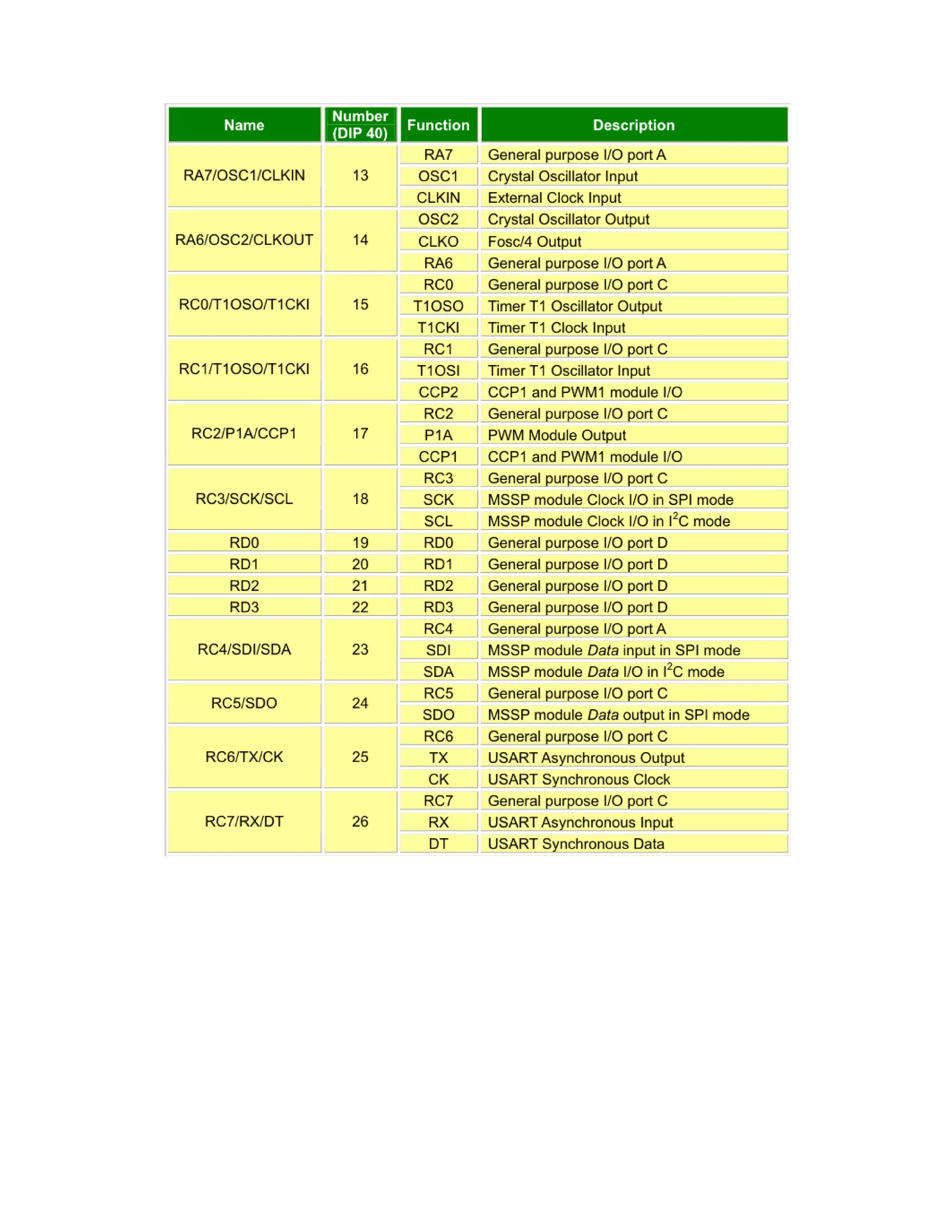
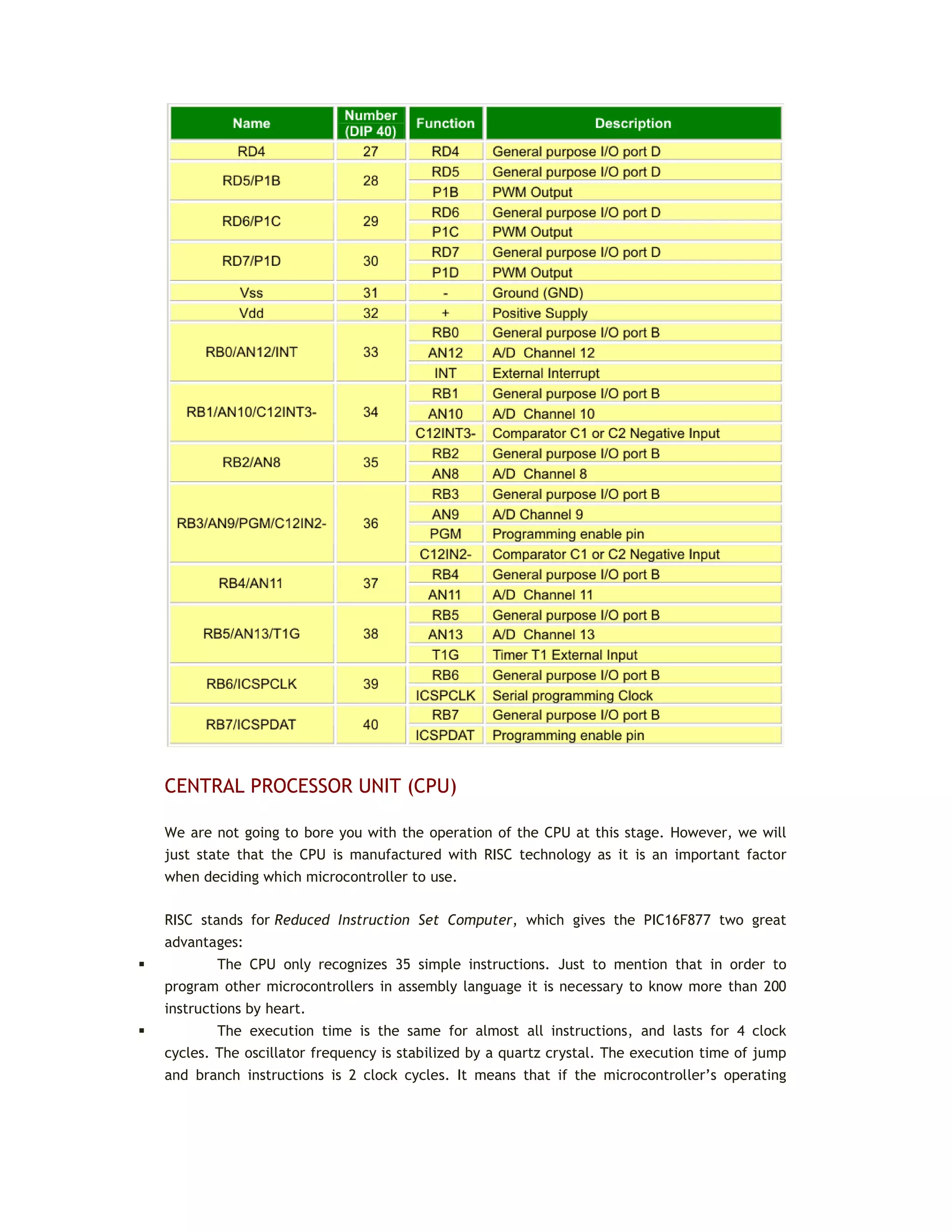
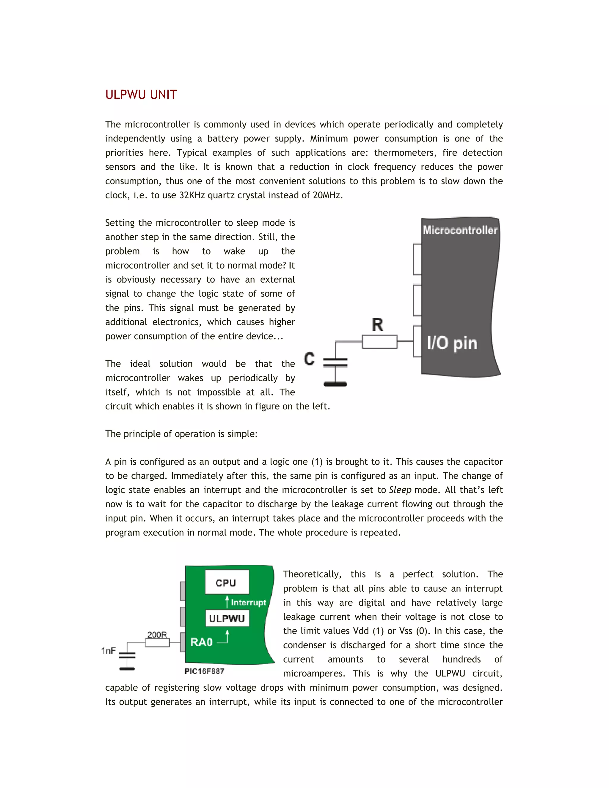
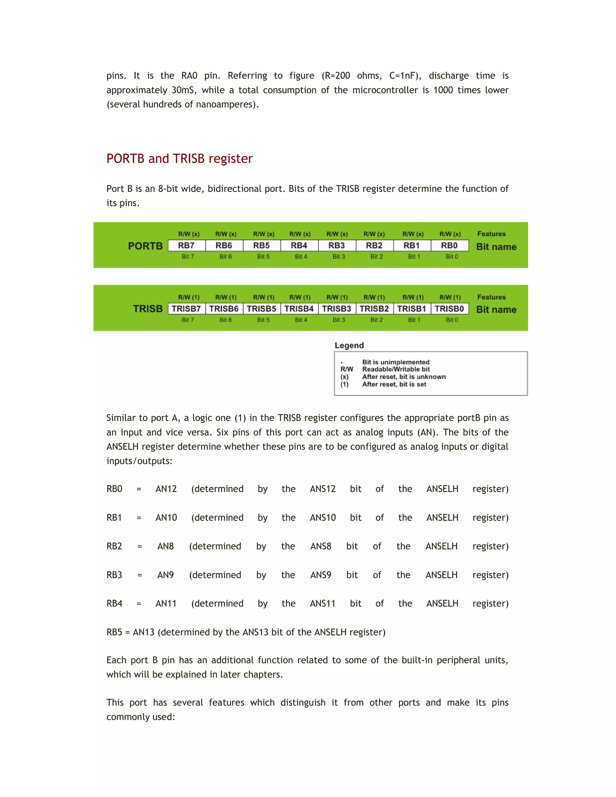
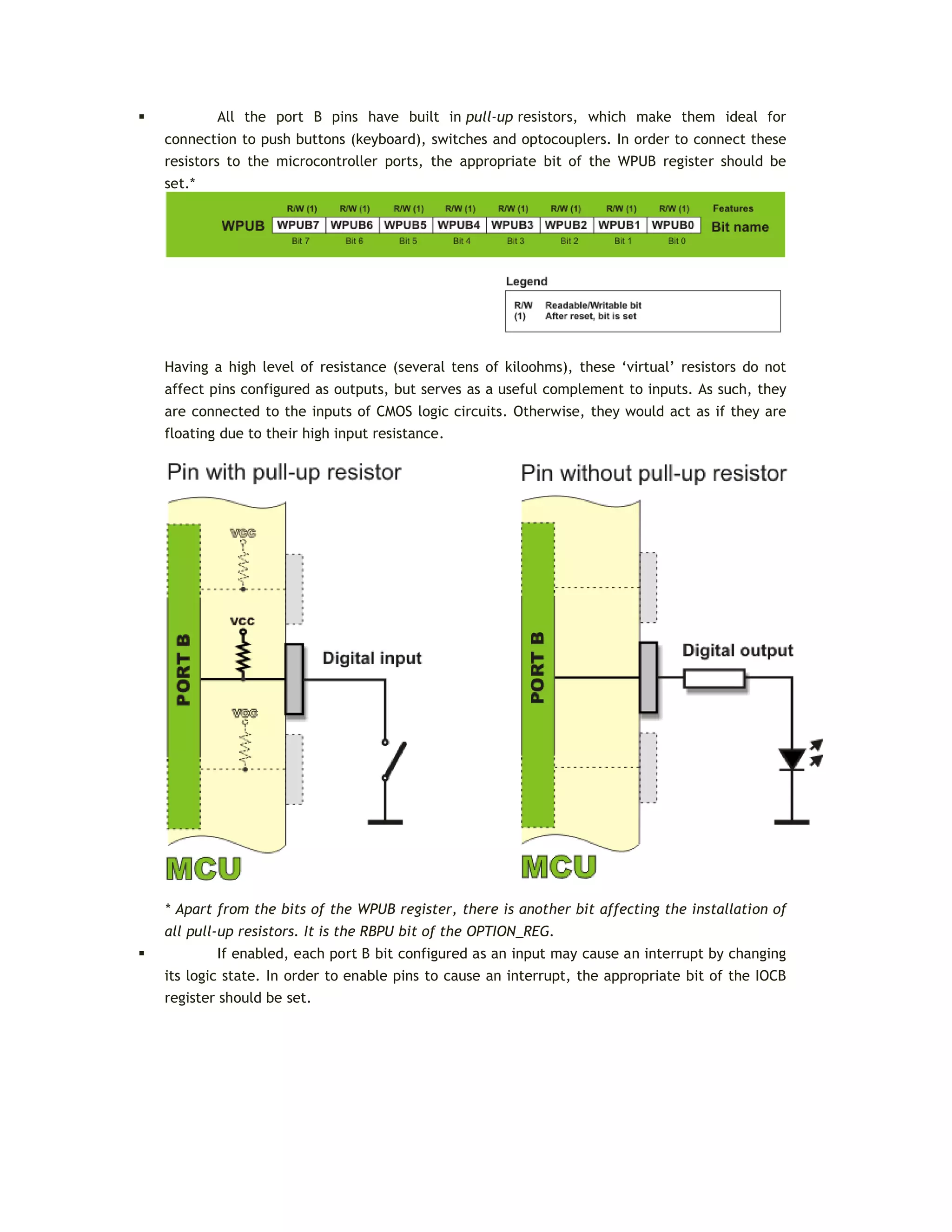
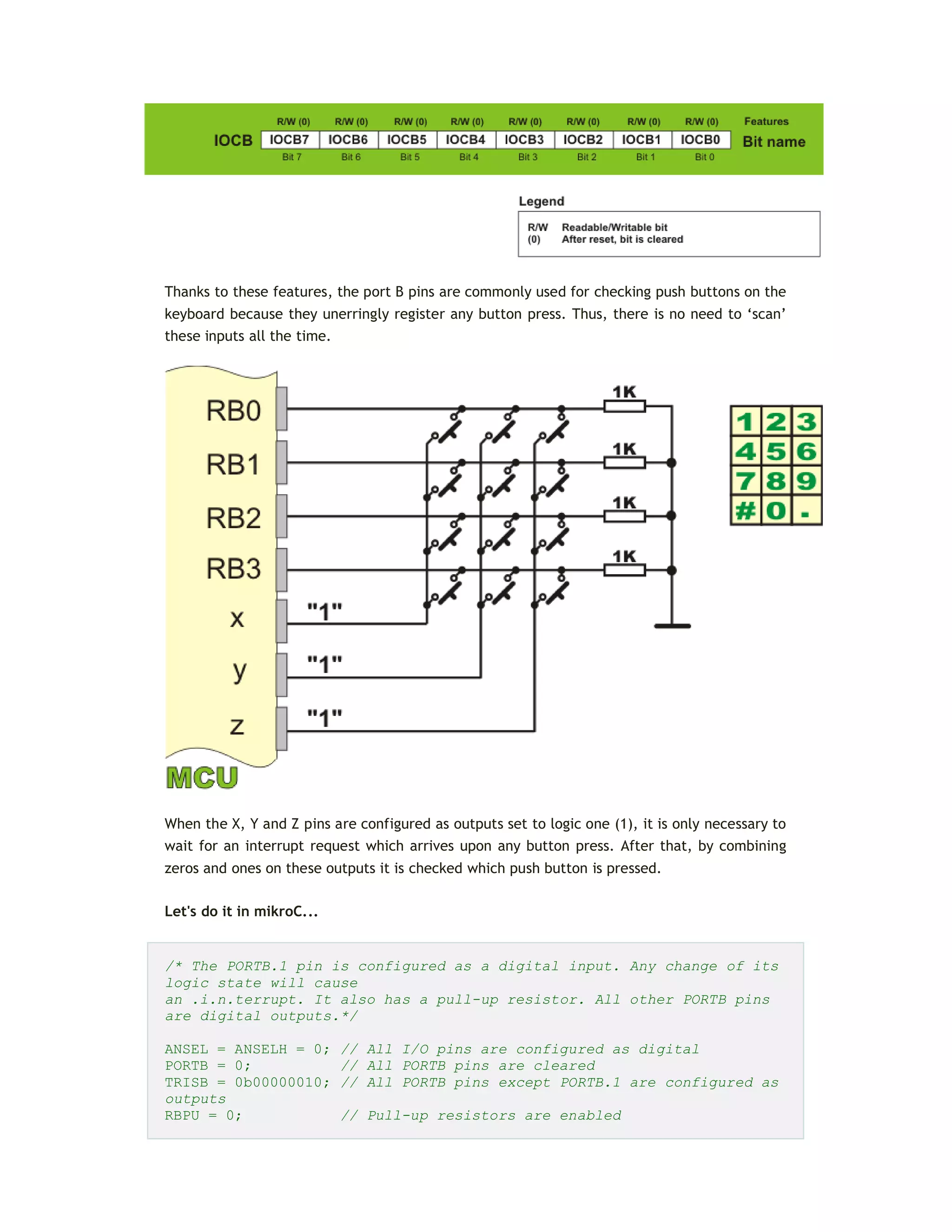
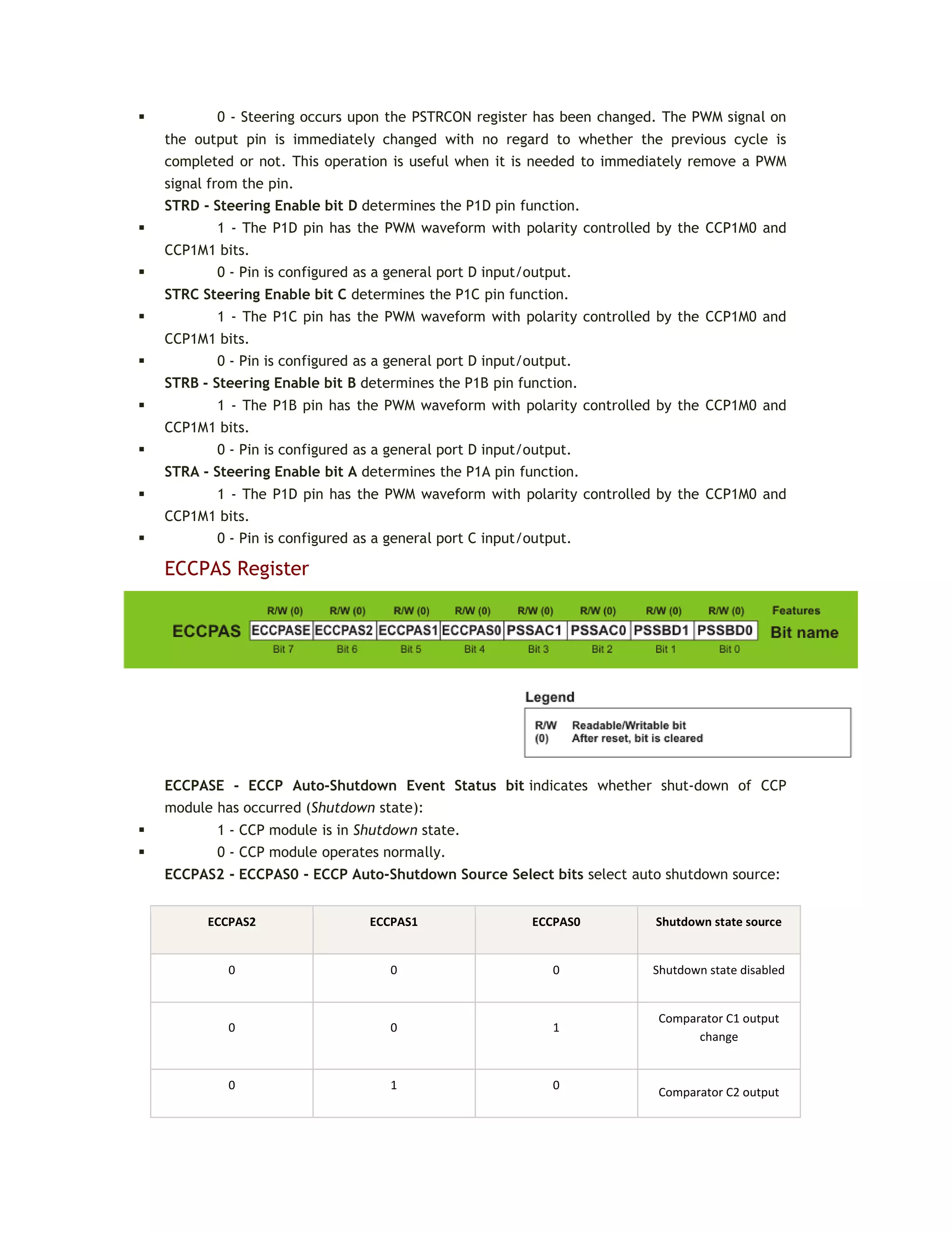
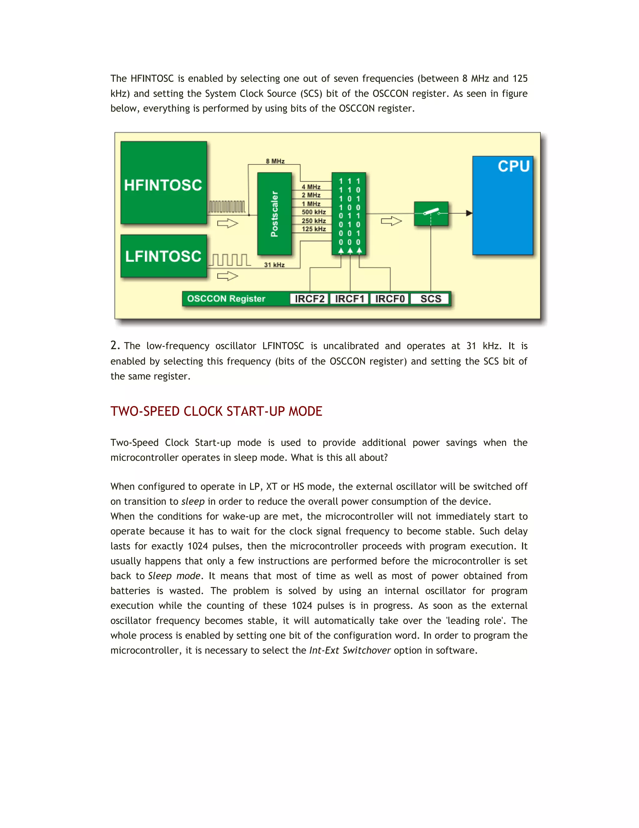
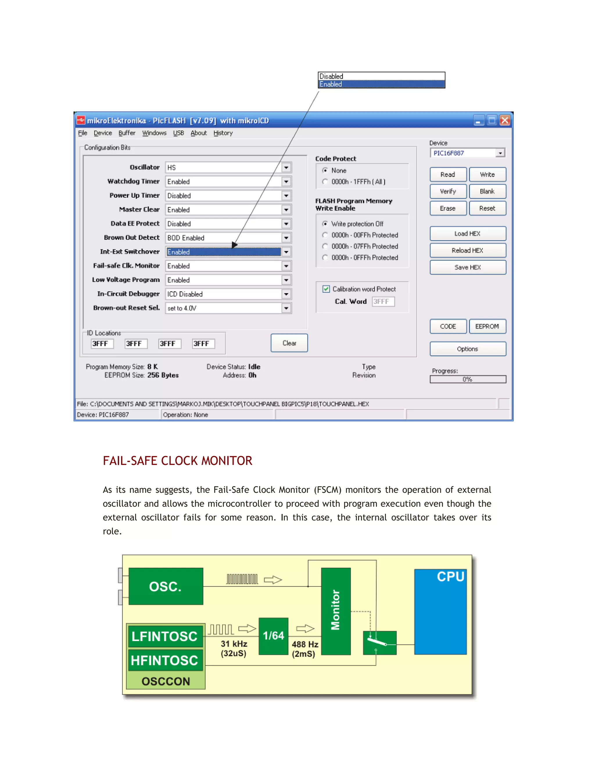
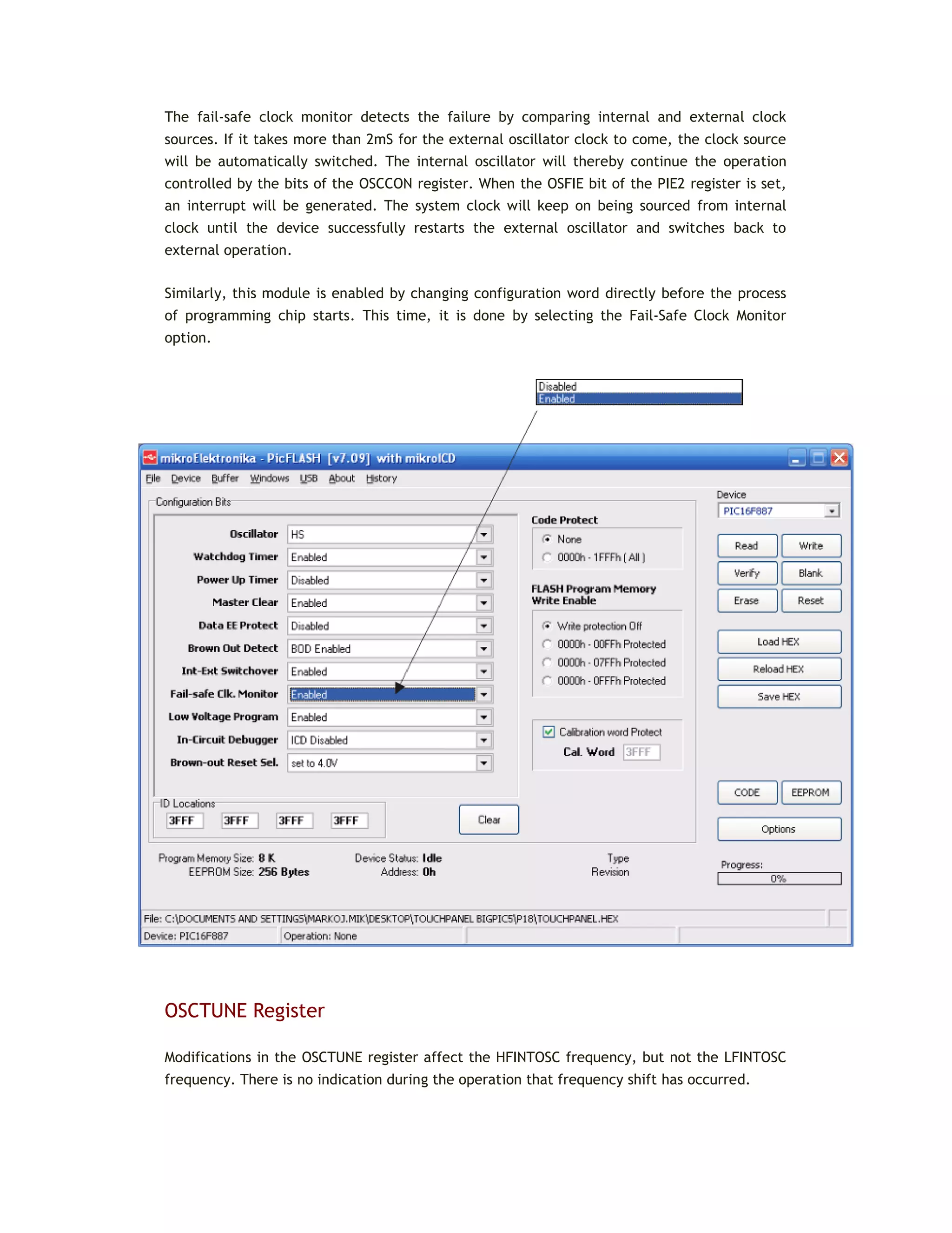
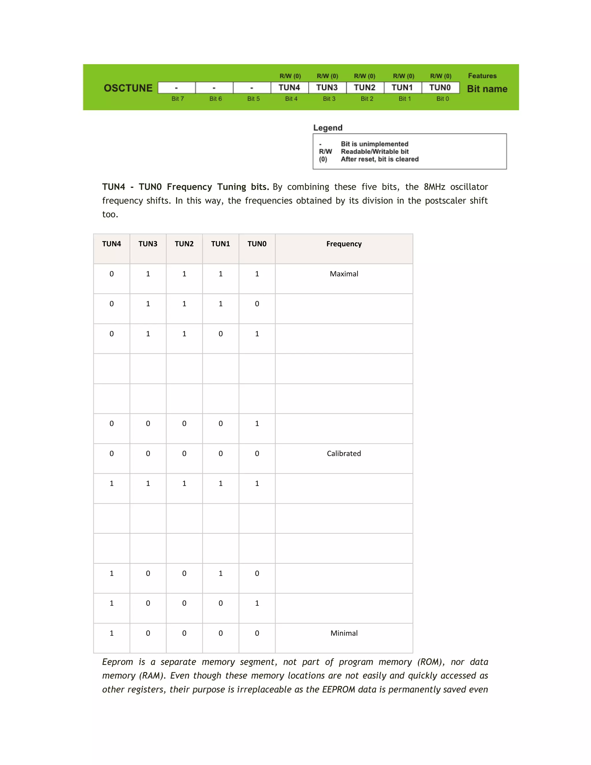
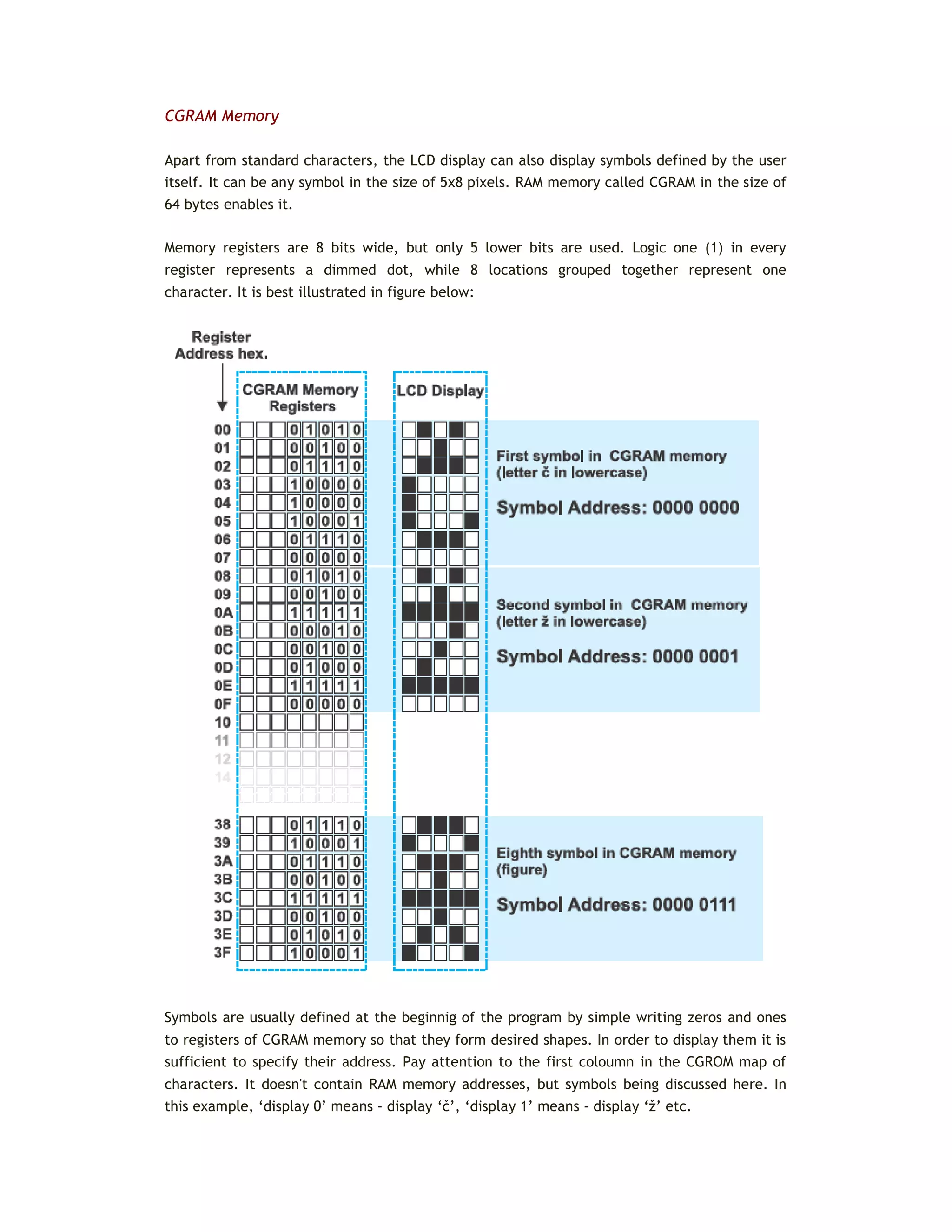
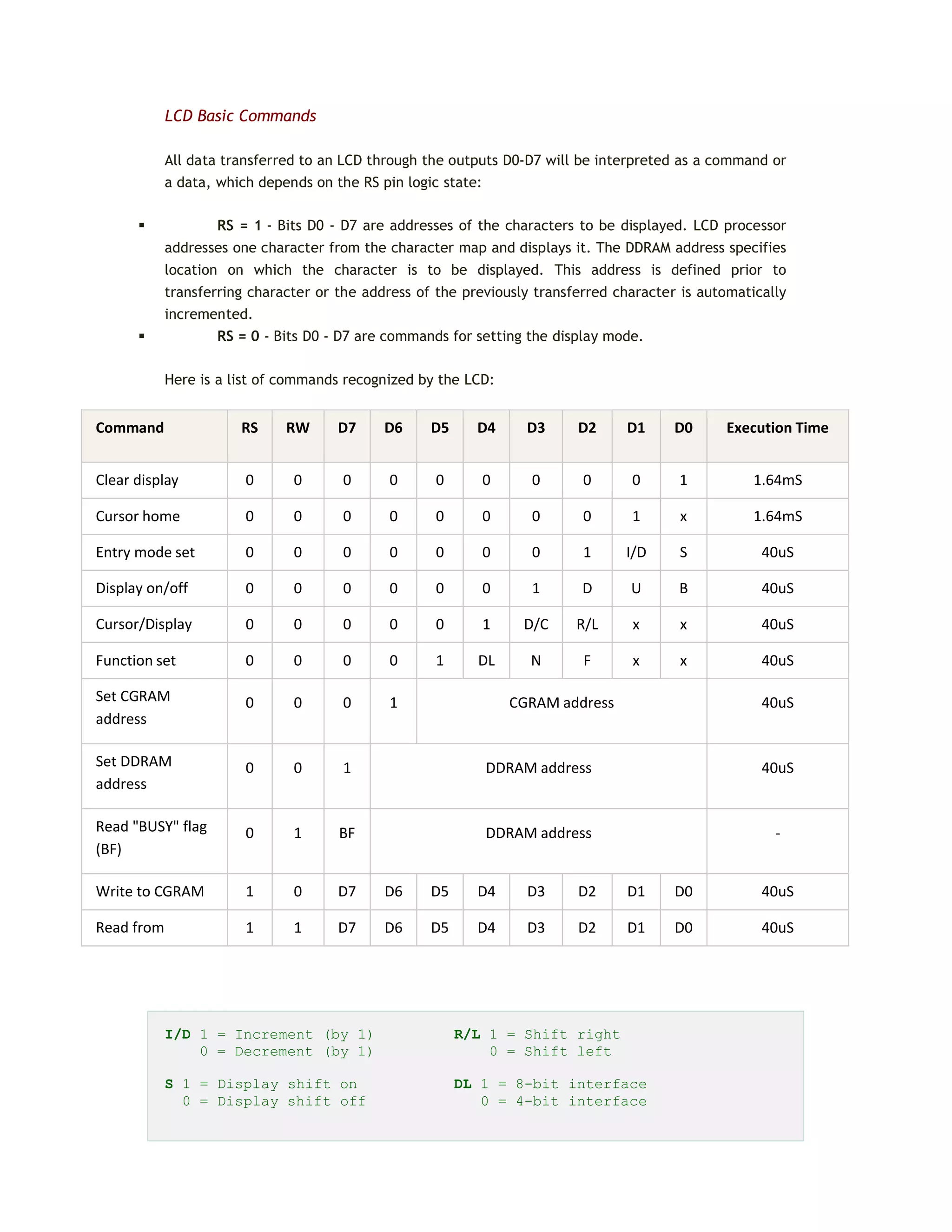
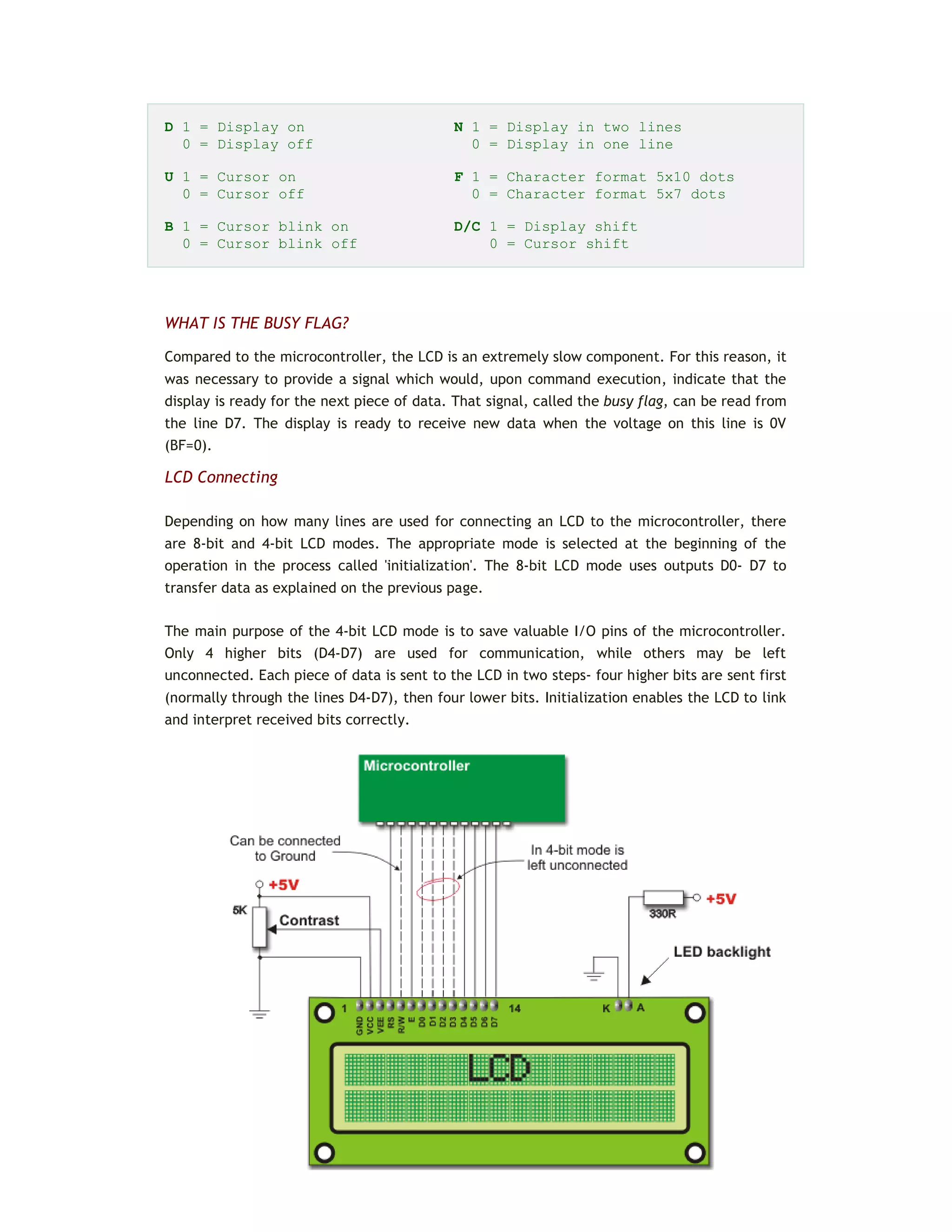
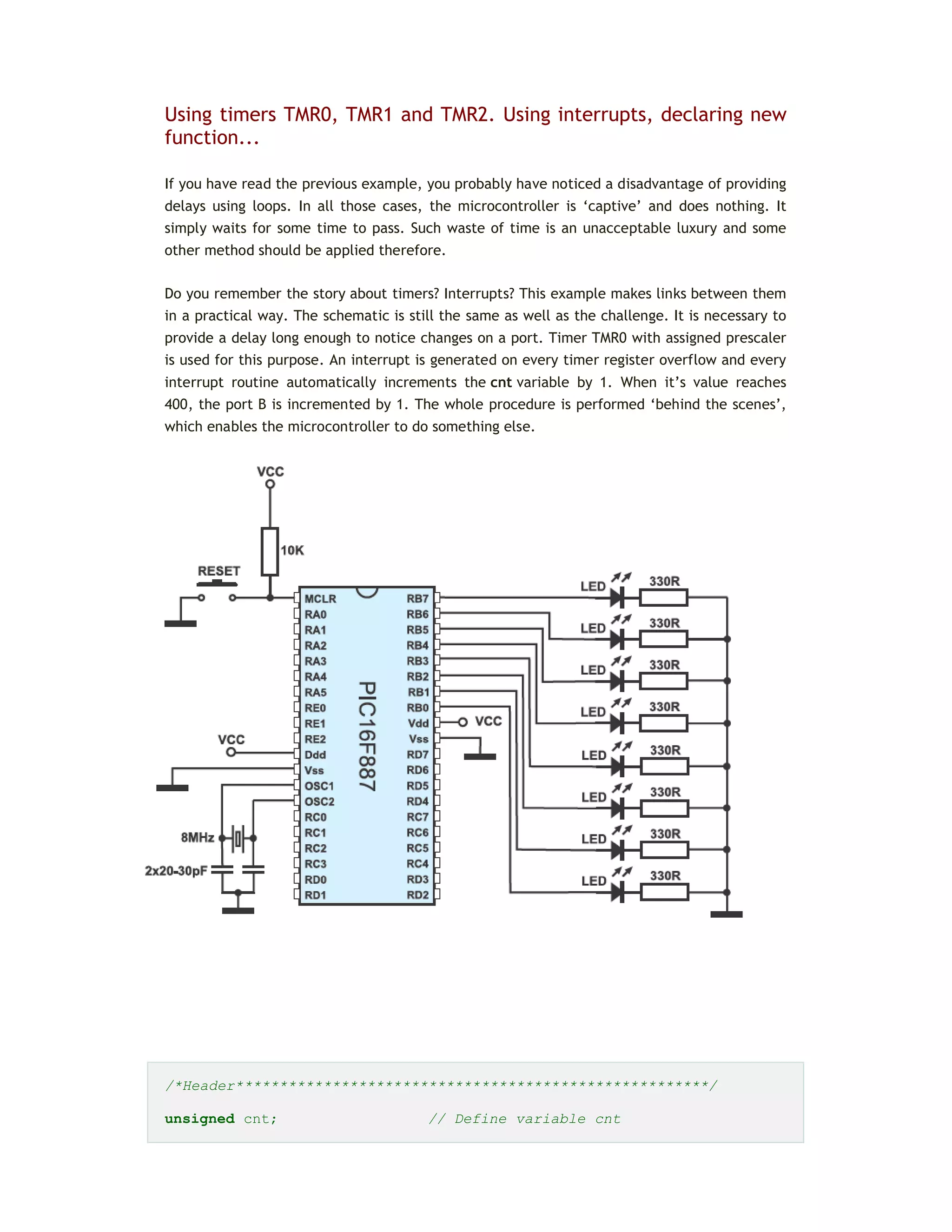
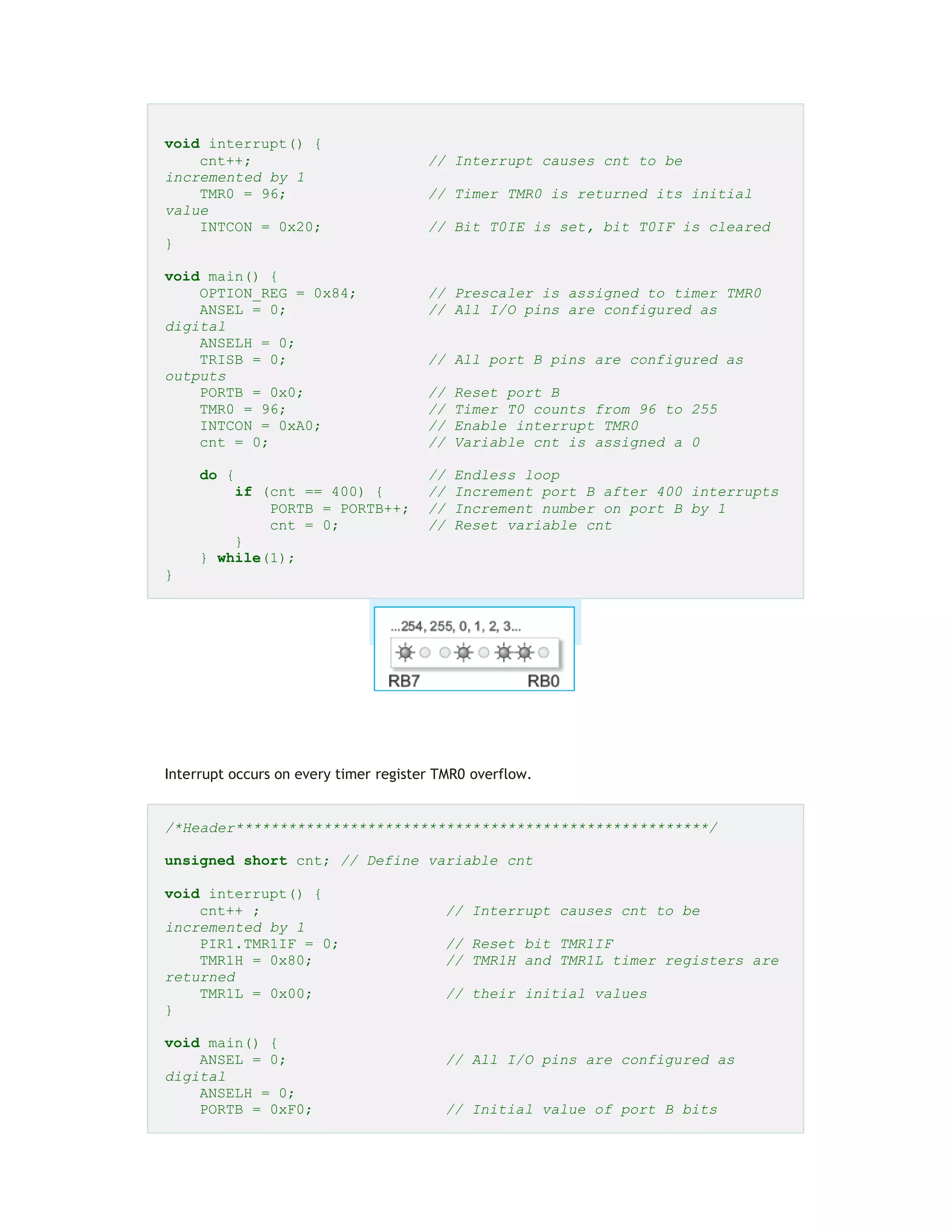
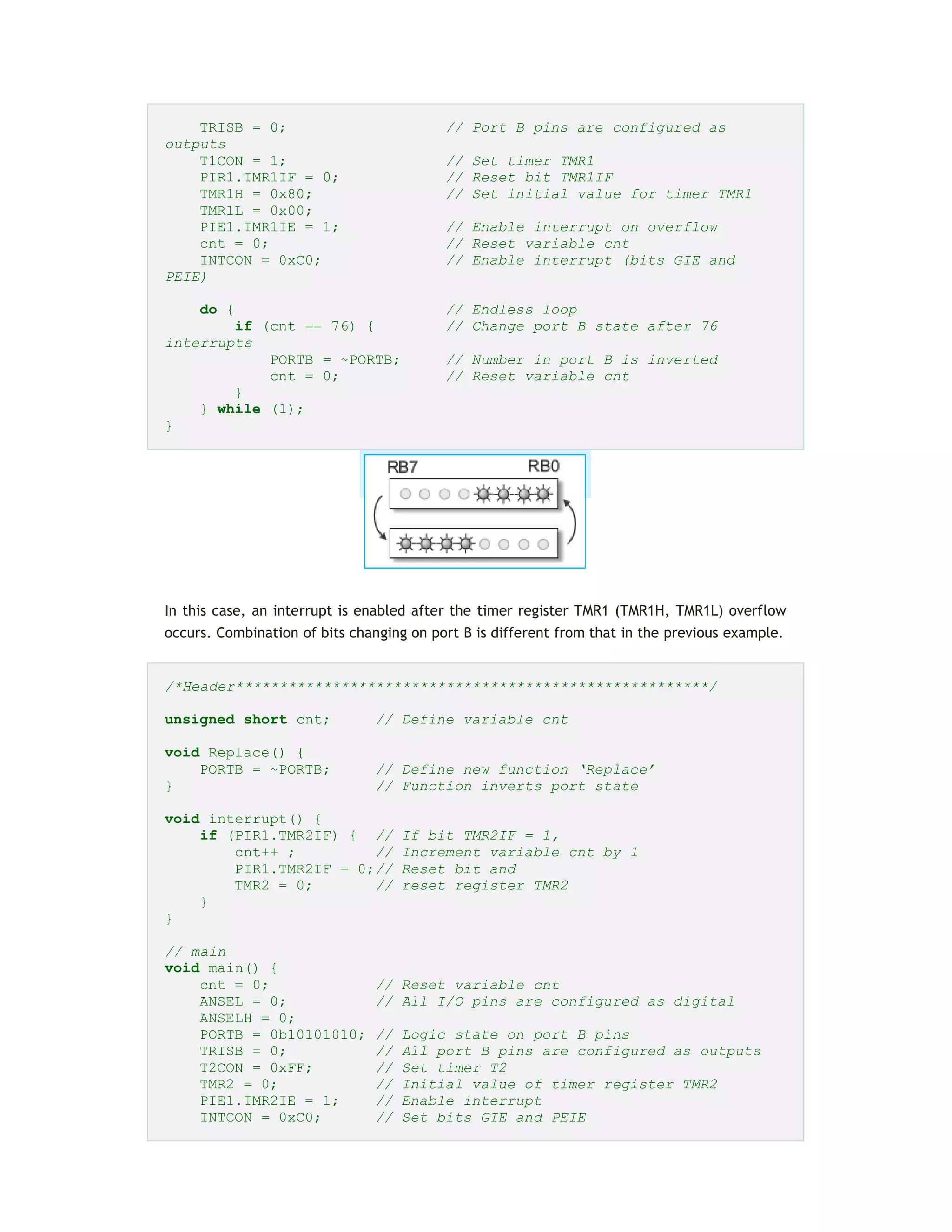
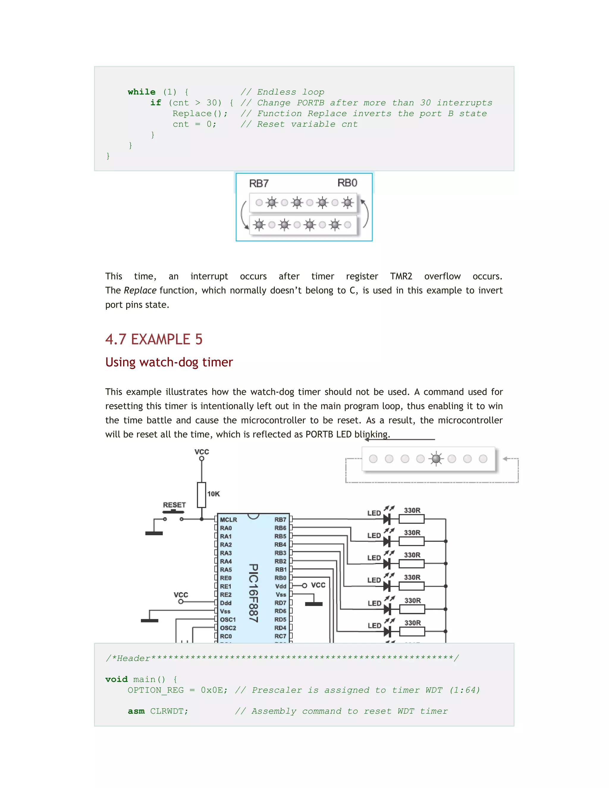
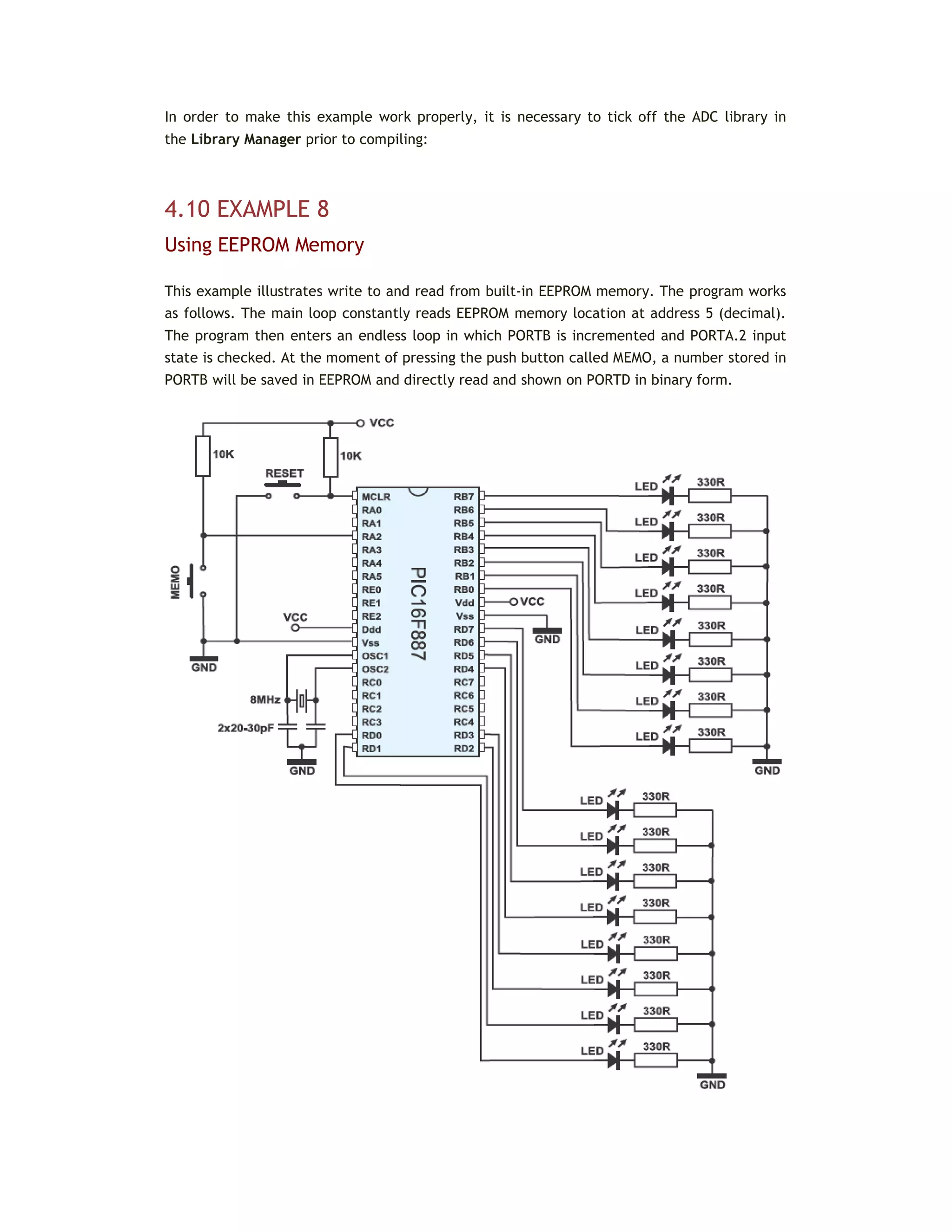
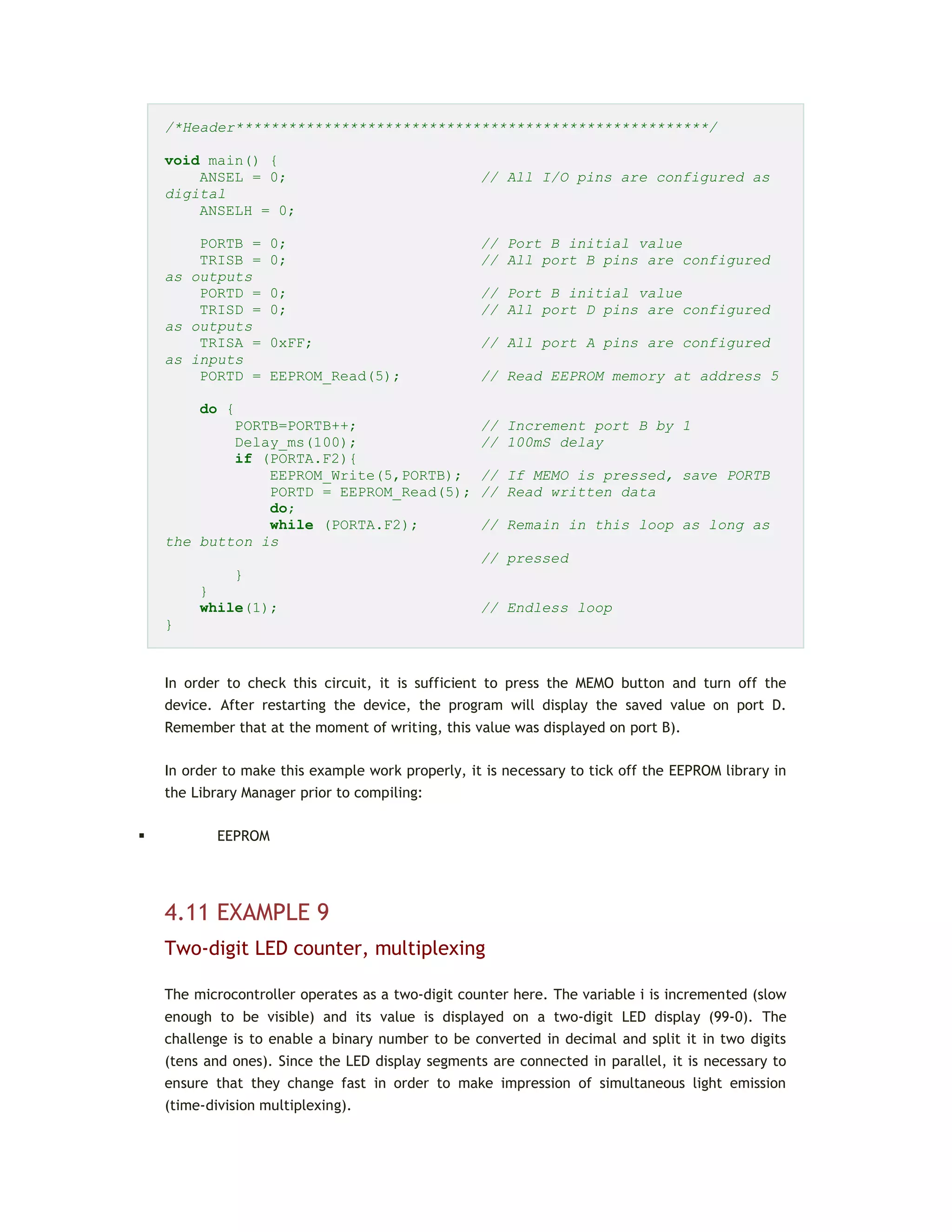
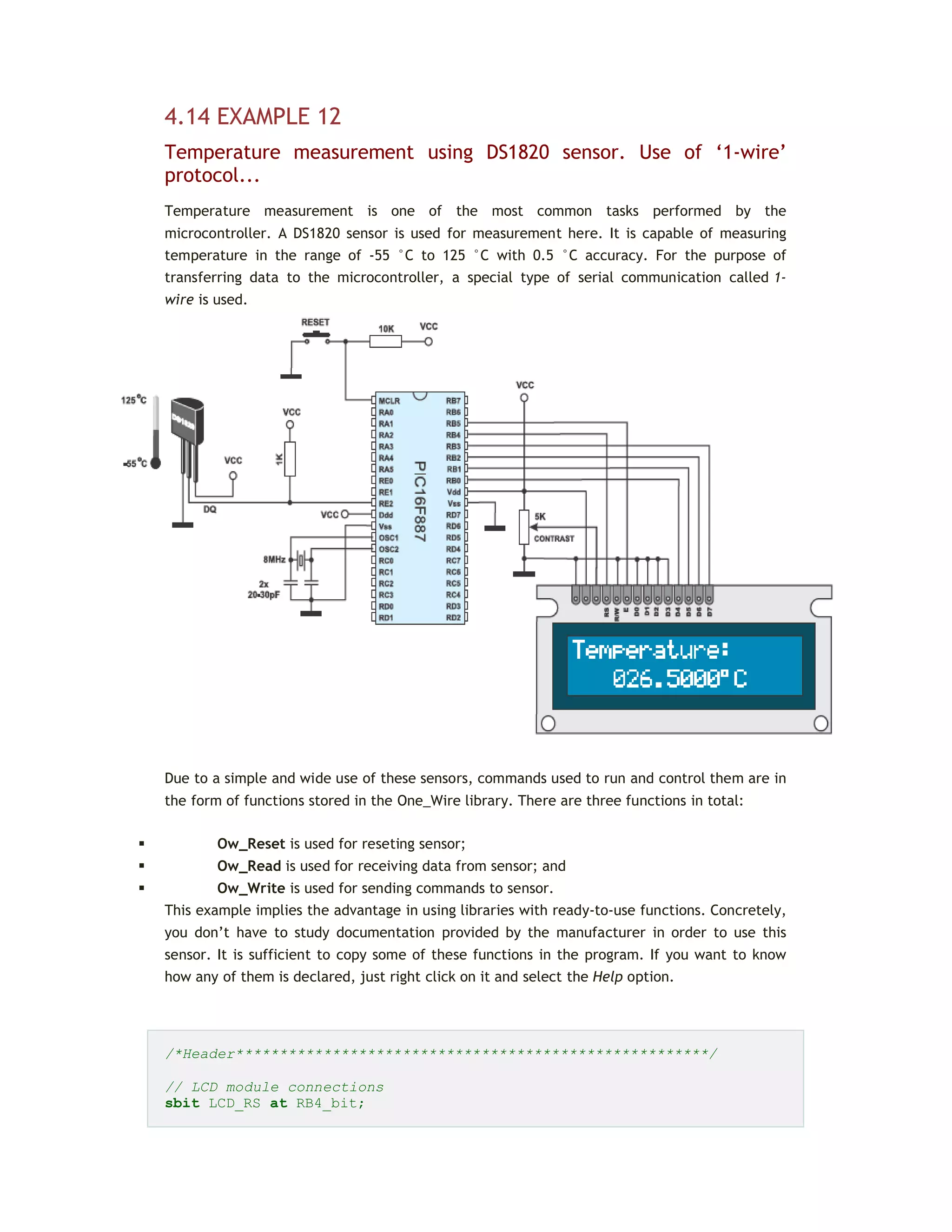
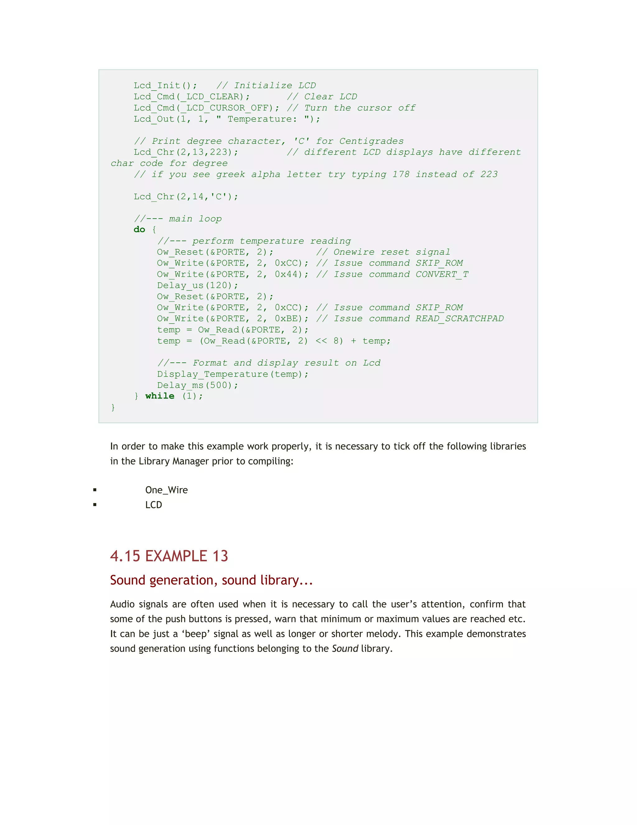
Download to read offline
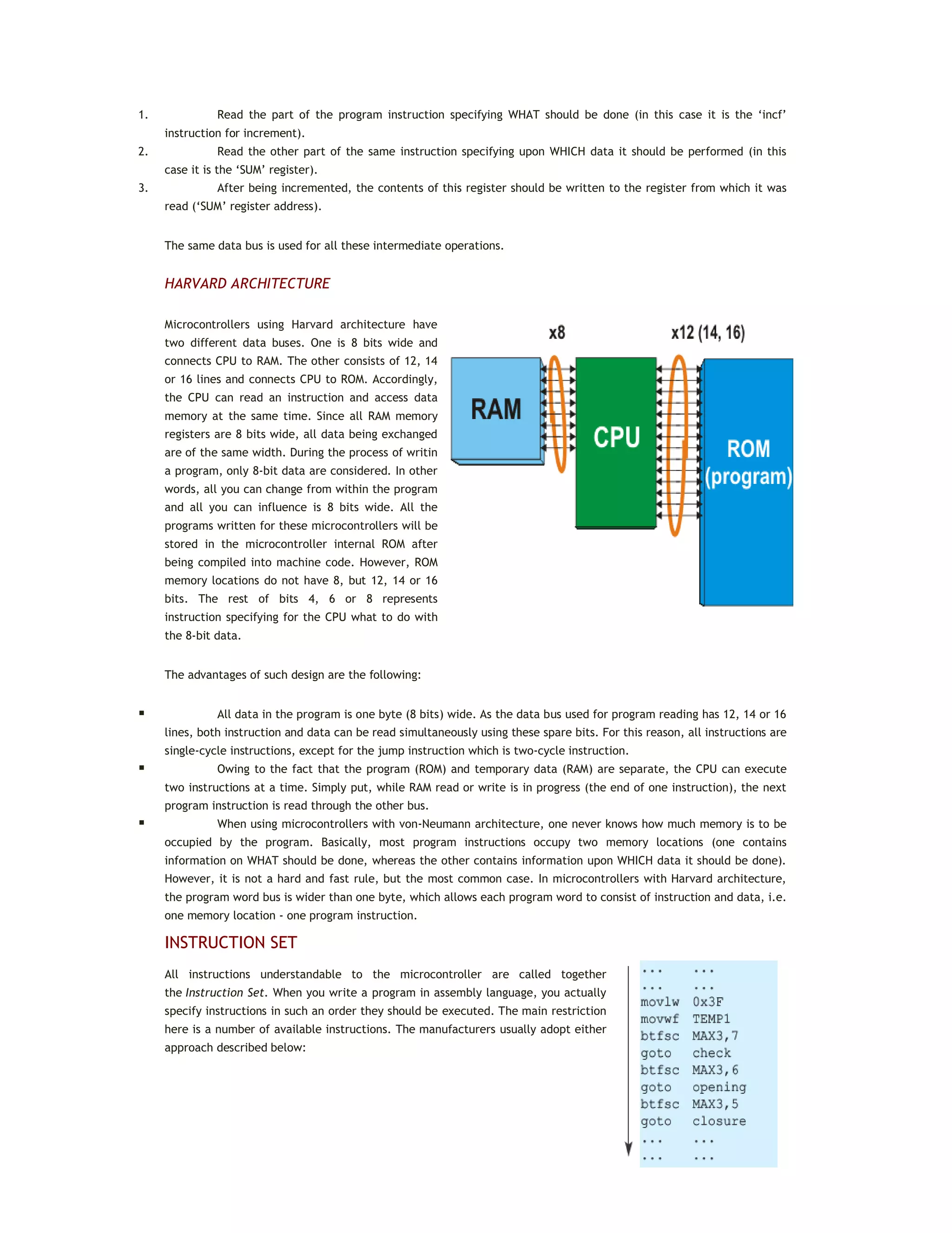
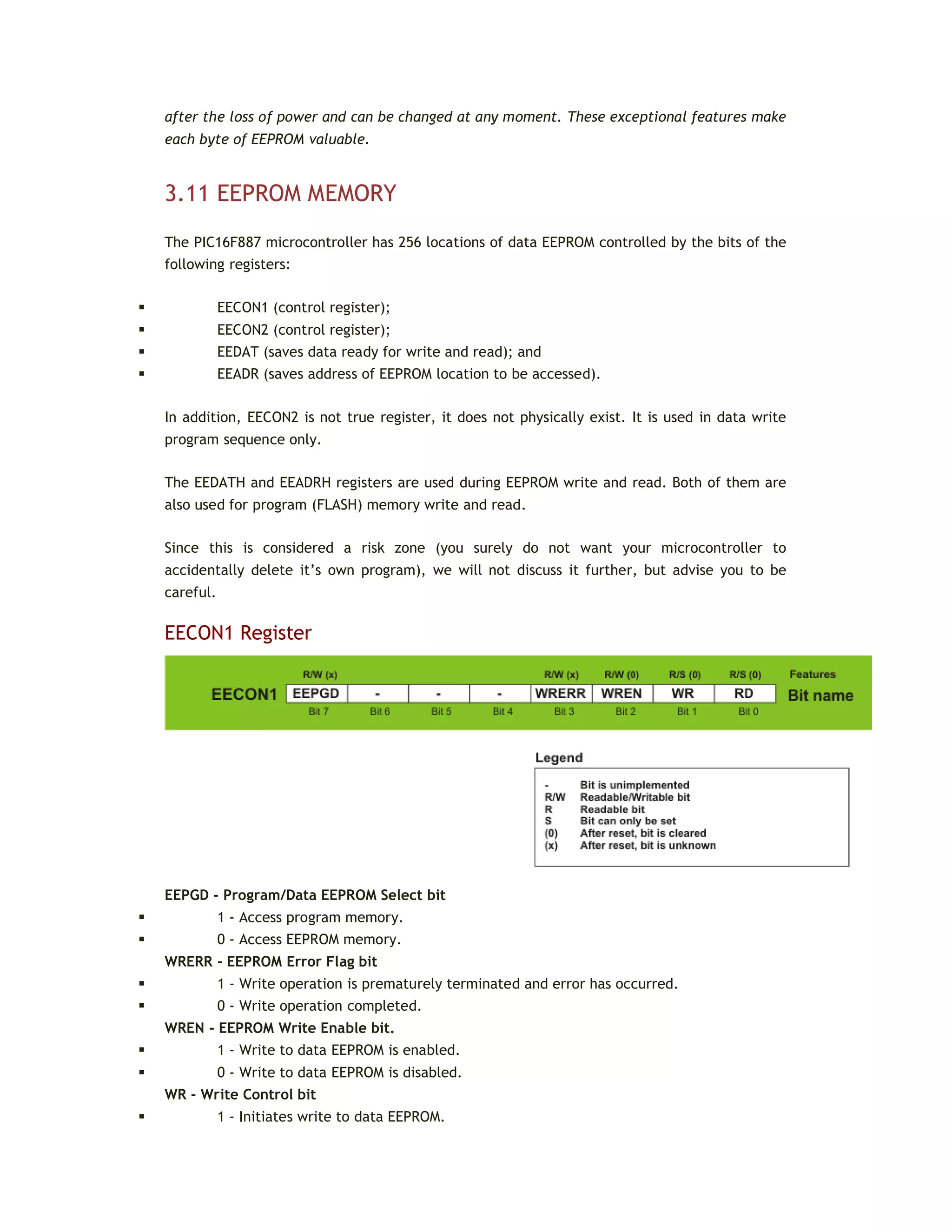
![between two devices on longer distances it is not possible to use parallel connection. Instead, serial communication
is used.
Today, most microcontrollers have built in several different systems for serial communication as a standard
equipment. Which of these systems will be used depends on many factors of which the most important are:
How many devices the microcontroller has to exchange data with?
How fast the data exchange has to be?
What is the distance between devices?
Is it necessary to send and receive data simultaneously?
One of the most important things concerning serial communication is the Protocol which should be strictly observed.
It is a set of rules which must be applied in order that devices can correctly interpret data they mutually exchange.
Fortunately, the microcontroller automatically takes care of this, so that the work of the programmer/user is
reduced to simple write (data to be sent) and read (received data).
BAUD RATE
The term baud rate is used to denote the number of bits transferred per second [bps]. Note that it refers to bits, not
bytes. It is usually required by the protocol that each byte is transferred along with several control bits. It means
that one byte in serial data stream may consist of 11 bits. For example, if the baud rate is 300 bps then maximum 37
and minimum 27 bytes may be transferred per second.
The most commonly used serial communication systems are:
I2
C (INTER INTEGRATED CIRCUIT)
Inter-integrated circuit is a system for serial data exchange between the microcontrollers and specialized integrated
circuits of a new generation. It is used when the distance between them is short (receiver and transmitter are usually
on the same printed board). Connection is established via two conductors. One is used for data transfer, the other is
used for synchronization (clock signal). As seen in figure below, one device is always a master. It performs addressing
of one slave chip before communication starts. In this way one microcontroller can communicate with 112 different
devices. Baud rate is usually 100 Kb/sec (standard mode) or 10 Kb/sec (slow baud rate mode). Systems with the baud
rate of 3.4 Mb/sec have recently appeared. The distance between devices which communicate over an I2C bus is
limited to several meters.](https://image.slidesharecdn.com/fmwc6ltijaekc37-210710214315/75/Microcontroladores-Programacion-del-microcontrolador-PIC-en-C-16-2048.jpg)
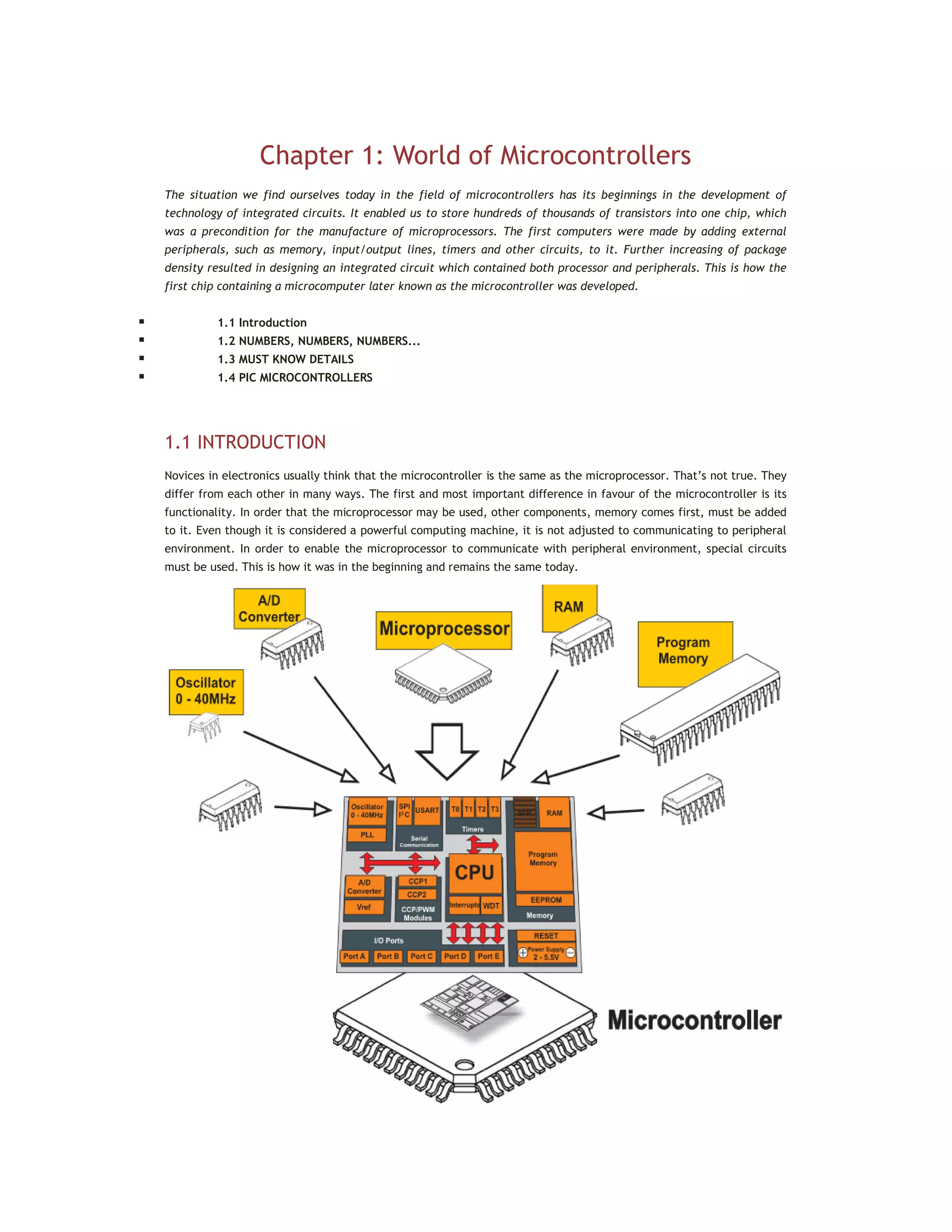
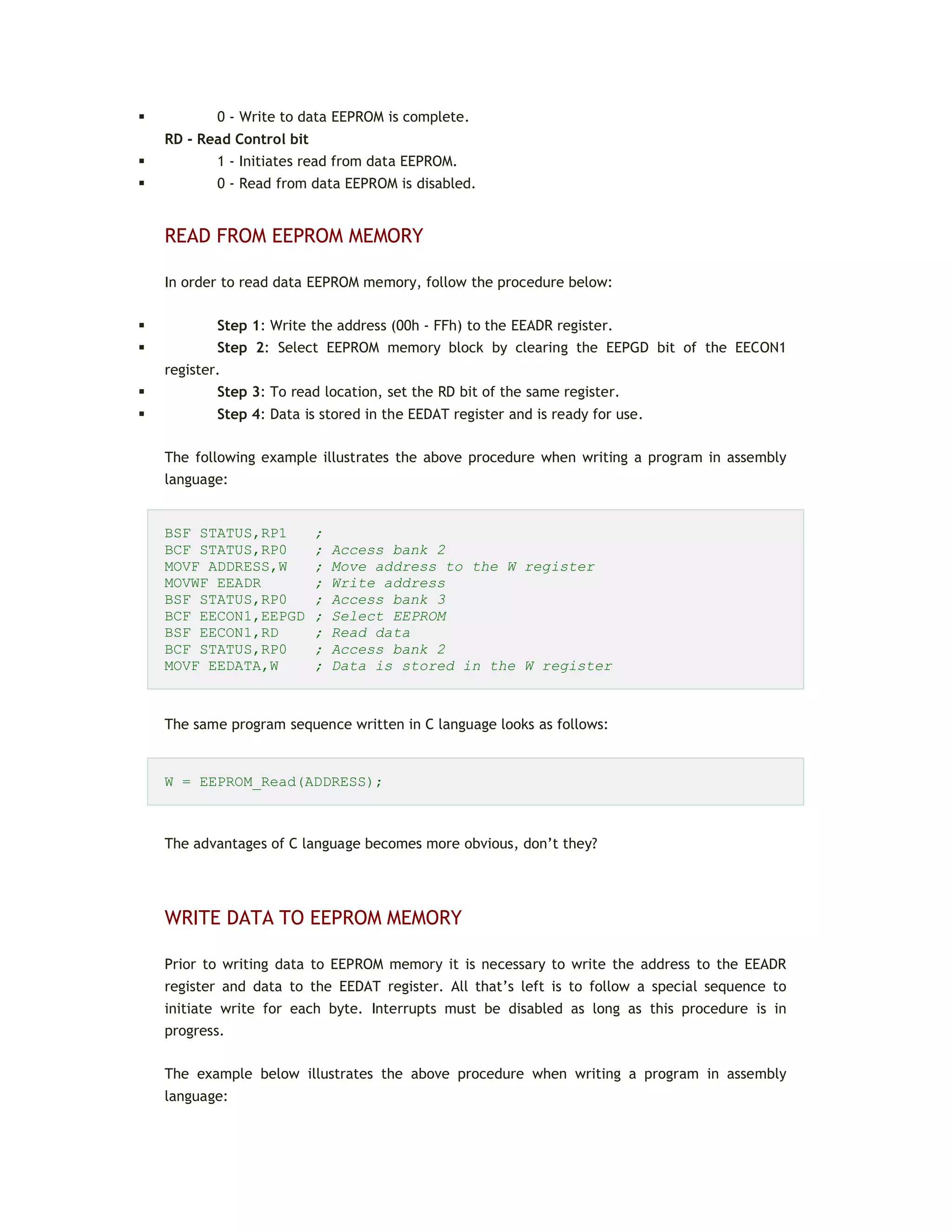
![Family
ROM
[Kbytes]
RAM
[bytes]
Pins
Clock
Freq.
[MHz]
A/D
Inputs
Resolution
of A/D
Converter
Compar-
ators
8/16 –
bit
Timers
Serial
Comm.
PWM
Outputs
Others
Base-Line 8 - bit architecture, 12-bit Instruction Word Length
PIC10FXXX
0.375 -
0.75
16 - 24 6 - 8 4 - 8 0 - 2 8 0 - 1 1 x 8 - - -
PIC12FXXX
0.75 -
1.5
25 - 38 8 4 - 8 0 - 3 8 0 - 1 1 x 8 - - EEPROM
PIC16FXXX 0.75 - 3
25 -
134
14 -
44
20 0 - 3 8 0 - 2 1 x 8 - - EEPROM
PIC16HVXXX 1.5 25
18 -
20
20 - - - 1 x 8 - -
Vdd =
15V
Mid-Range 8 - bit architecture, 14-bit Instruction World Length
PIC12FXXX
1.75 -
3.5
64 -
128
8 20 0 - 4 10 1
1 - 2 x 8
1 x 16
- 0 - 1 EEPROM
PIC12HVXXX 1.75 64 8 20 0 - 4 10 1
1 - 2 x 8
1 x 16
- 0 - 1 -
PIC16FXXX
1.75 -
14
64 -
368
14 -
64
20 0 - 13 8 or 10 0 - 2
1 - 2 x 8
1 x 16
USART I2C
SPI
0 - 3 -
PIC16HVXXX
1.75 -
3.5
64 -
128
14 -
20
20 0 - 12 10 2
2 x 8 1
x 16
USART I2C
SPI
- -
High-End 8 - bit architecture, 16-bit Instruction Word Length
PIC18FXXX 4 - 128
256 -
3936
18 -
80
32 - 48 4 - 16 10 or 12 0 - 3
0 - 2 x 8
2 - 3 x
16
USB2.0
CAN2.0
USART I2C
SPI
0 - 5 -
PIC18FXXJXX 8 - 128
1024 -
3936
28 -
100
40 - 48
10 -
16
10 2
0 - 2 x 8
2 - 3 x
16
USB2.0
USART
Ethernet
I2C SPI
2 - 5 -
PIC18FXXKXX 8 - 64
768 -
3936
28 -
44
64
10 -
13
10 2
1 x 8 3
x 16
USART I2C
SPI
2 -
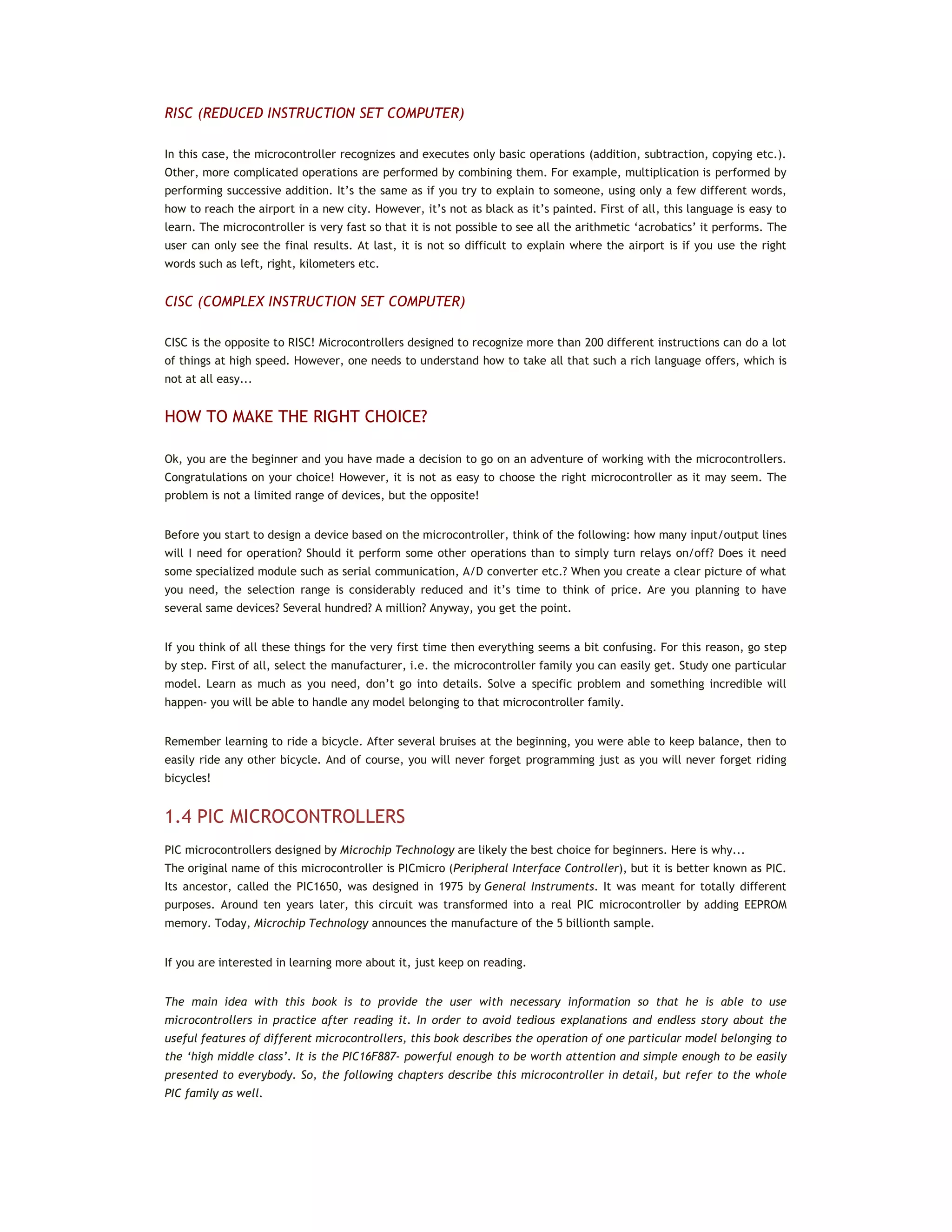
All PIC microcontrollers use Harvard architecture, which means that their program memory is connected to the CPU
over more than 8 lines. Depending on the bus width, there are 12-, 14- and 16-bit microcontrollers. Table above
shows the main features of these three categories.](https://image.slidesharecdn.com/fmwc6ltijaekc37-210710214315/75/Microcontroladores-Programacion-del-microcontrolador-PIC-en-C-24-2048.jpg)
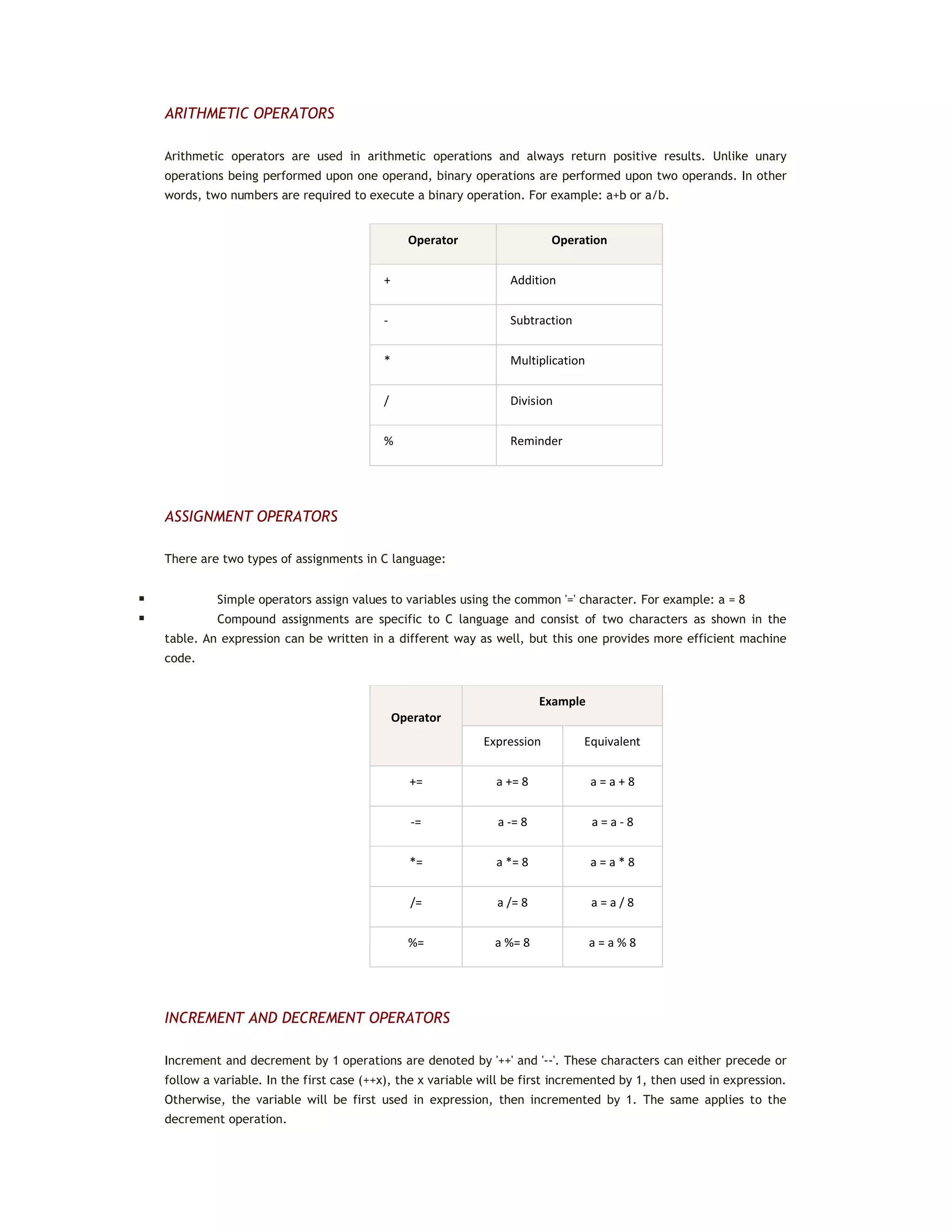
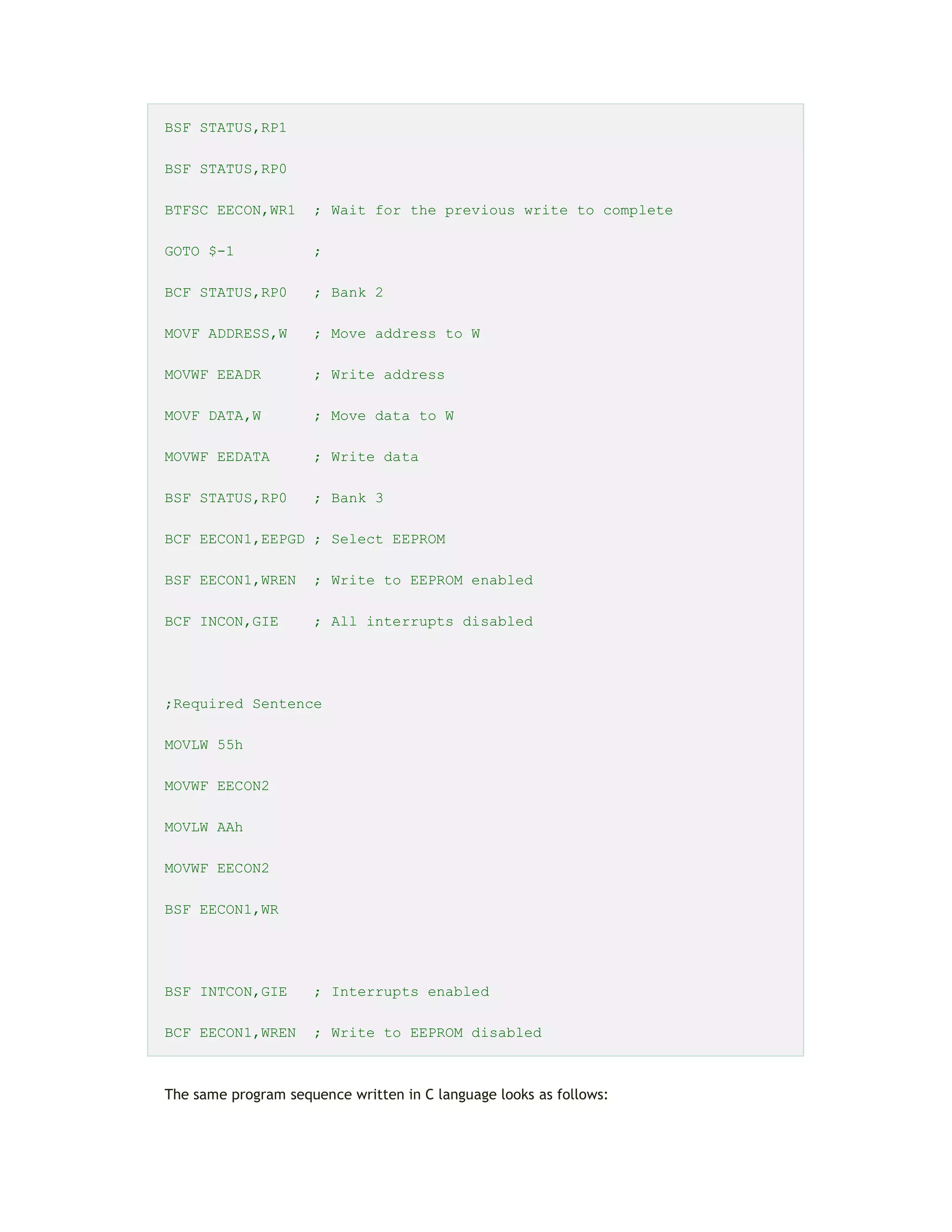
![| Bitwise OR c = a | b a = 11100011
b = 11001100
c = 11101111
^ Bitwise EXOR c = a ^ b a = 11100011
b = 11001100
c = 00101111
HOW TO USE OPERATORS?
Except for assignment operators, two operators must not be written next to each other.
x*%12; // such expression will generate an error
Operators are grouped together using parentheses similar to arithmetic expressions. The expressions
enclosed within parentheses are calculated first. If necessary, multiple (nested) parentheses can be used.
Each operator has its priority and associativity as shown in the table.
Priority Operators Associativity
High () [] -> . from left to right
! ~ ++ -- +(unary) -(unary) *Pointer &Pointer from right to left
* / % from left to right
+ - from left to right
< > from left to right
< <= > >= from left to right
== != from left to right
& from left to right
^ from left to right
| from left to right
&& from left to right
|| from right to left
?: from right to left
Low = += -= *= /= /= &= ^= |= <= >= from left to right](https://image.slidesharecdn.com/fmwc6ltijaekc37-210710214315/75/Microcontroladores-Programacion-del-microcontrolador-PIC-en-C-42-2048.jpg)

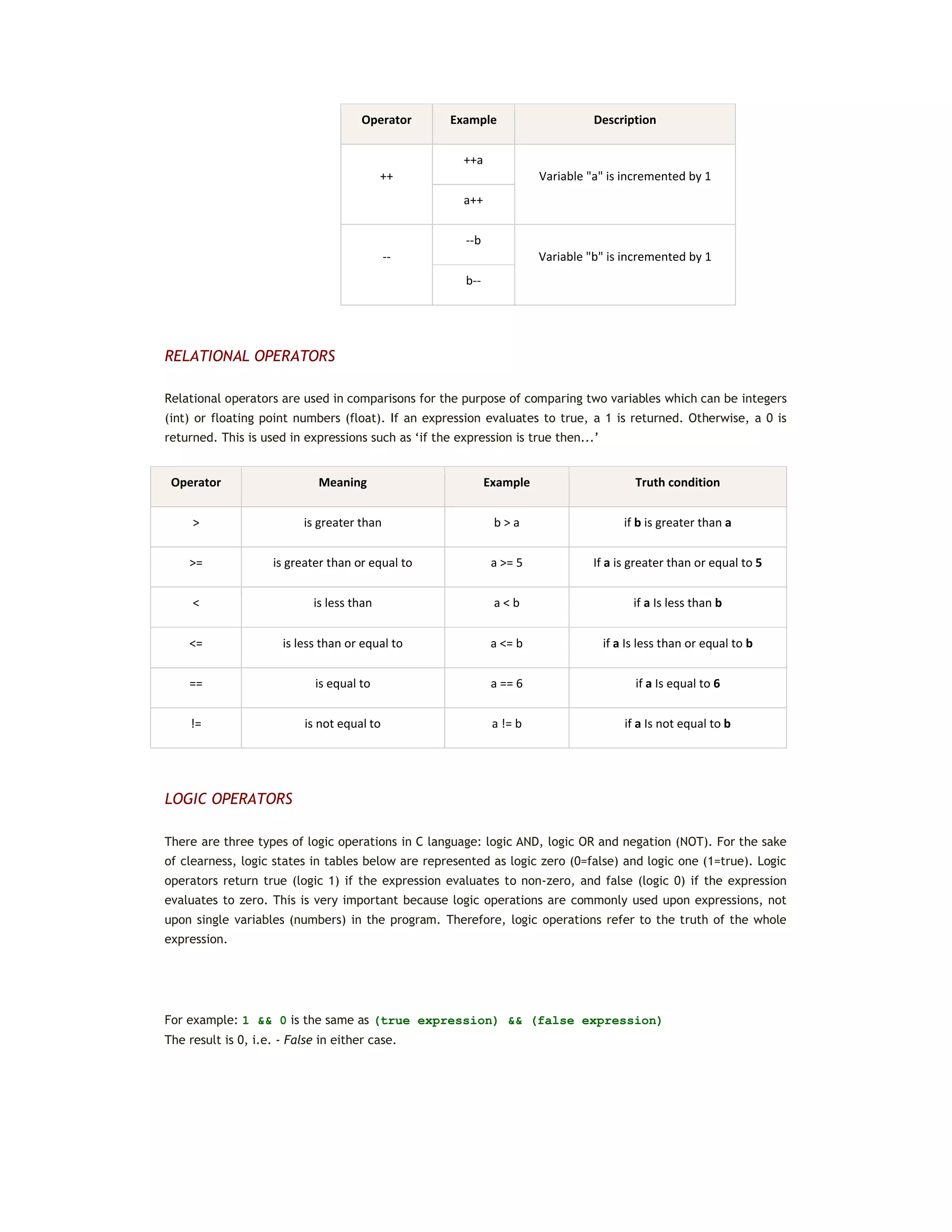
![Sometimes the process of writing a
program in C language requires parts
of the code to be written in assembly
language. This enables complicated
parts of the program to be executed
in a precisely defined way for exact
period of time. For example, when it
is necessary to have very short pulses
(a few microseconds) appearing
periodically on a microcontroller pin.
In such and similar cases, the simplest
solution is to use assembly code for
the part of the program controlling
pulse duration.
One or more assembly instructions are inserted in the program written in C language using the asm command:
asm
{
Assembly language instructions
...
}
Codes written in assembly language can use constants and variables previously defined in C language. Of
course, as the whole program is written in C language, the rules thereof are applied when declaring these
constants and variables.
unsigned char maximum = 100; // Declare variables: maximum = 100
asm
{ // Start of assembly code
MOVF maximum,W // W = maximum = 100
...
} // End of assembly code
ARRAYS
A group of variables of the same type is called an array. Elements of an array are called components, while
their type is called the main type. An array is declared by specifying its name, type and the number of
elements it will comprise:
component_type array_name [number_of_components];
Such a complicated definition for something so simple, isn’t it? An array can be thought of as a shorter or
longer list of variables of the same type where each of these is assigned an ordinal number (numbering always
starts at zero). Such an array is often called a vector. The figure below shows an array named shelf which
consists of 100 elements.](https://image.slidesharecdn.com/fmwc6ltijaekc37-210710214315/75/Microcontroladores-Programacion-del-microcontrolador-PIC-en-C-47-2048.jpg)
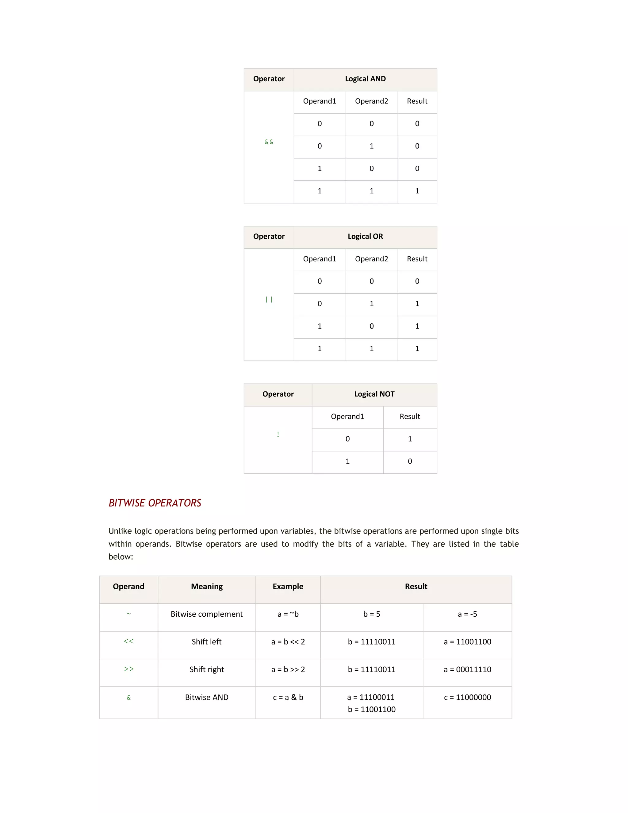
![Array "shelf" Elements of array Contents of element
7 shelf[0] 7
23 shelf[1] 23
34 shelf[2] 34
0 shelf[3] 0
0 shelf[4] 0
12 shelf[5] 12
9 shelf[6] 9
... ... ...
... ... ...
23 shelf [99] 23
In this case, the contents of a variable (an element of the array) represents a number of products the shelf
contains. Elements are accessed by indexing, i.e. by specifying their ordinal number (index):
shelf[4] = 12; // 12 items is ‘placed’ on shelf [4]
temp = shelf [1]; // Variable shelf[1] is copied to
// variable temp
Elements can be assigned contents during array declaration. In the following example, the array named
calendar is declared and each element is assigned specific number of days:
unsigned char calendar [12] = {31,28,31,30,31,30,31,31,30,31,30,31};
TWO-DIMENSIONAL ARRAY
Apart from one-dimensional arrays which could be thought of as a list, there are also multidimensional arrays
in C language. In a few following sentences we are going to describe only two-dimensional arrays
called matrices which can be thought of as tables. A twodimensional array is declared by specifying data type
of the array, the array name and the size of each dimension. Look at the example below:
component_type array_name [number_of_rows] [number_of_columns];
number_of_rows and number_of_columns represent the number of rows and columns of a table, respectively.
int Table [3][4]; // Table is defined to have 3 rows and 4 columns
This array can be represented in the form of a table.](https://image.slidesharecdn.com/fmwc6ltijaekc37-210710214315/75/Microcontroladores-Programacion-del-microcontrolador-PIC-en-C-48-2048.jpg)
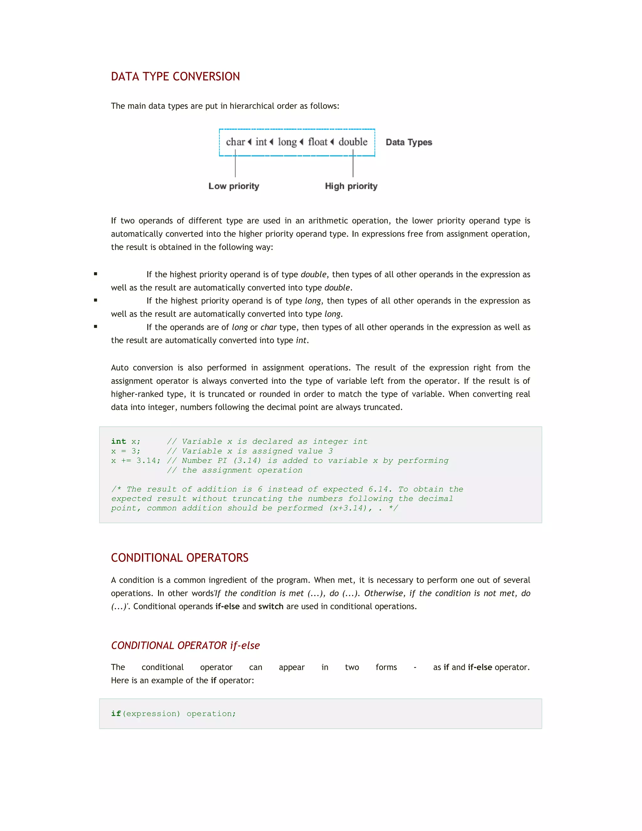
![table[0][0] table[0][1] table[0][2] table[0][3]
table[1][0] table[1][1] table[1][2] table[1][3]
table[2][0] table[2][1] table[2][2] table[2][3]
Similar to vectors, the elements of a matrix can be assigned values during array declaration. In the following
example, the elements of the two-dimensional array Table are assigned values. As seen, this array has two
rows and three columns:
int Table[2][3] = {{3,42,1}, {7,7,19}};
The matrix above can also be represented in the form of a table the elements of which have the following
values:
FUNCTIONS
Every program written in C language consists of larger or smaller number of functions. The main idea is to
divide a program into several parts using these functions in order to solve the actual problem easier. Besides,
functions enable us to use the skills and knowledge of other programmers. For example, if it is necessary to
send a string to an LCD display, it is much easier to use already written part of the program than to start over.
Functions consist of commands specifying what should be done upon variables. They can be compared to
subroutines. As a rule, it is much better to have a program consisting of large number of simple functions than
of a few large functions. A function body usually consists of several commands being executed by the order
they are specified.
Every function must be properly declared so as to be properly interpreted during the process of compilation.
Declaration contains the following elements:
Function name
Function body
List of parameters
Declaration of parameters
Type of function result
This is how a function looks like:
type_of_result function_name (type argument1, type argument2,...)
{
Command;
3 42 1
7 7 19](https://image.slidesharecdn.com/fmwc6ltijaekc37-210710214315/75/Microcontroladores-Programacion-del-microcontrolador-PIC-en-C-49-2048.jpg)
![IDE FOR MIKROC PRO FOR PIC
This is what you get when you start up IDE for mikroC PRO for PIC for the very first time:
Unfortunately, a detailed description of all the options available in this compiler would take too much of our
time, so that we are going to skip it. Instead, we are going to describe only the process of writing a program in
C language, simulator checking as well as its loading into the microcontroller memory. For more information
refer to help [F1].
PROJECT MANAGER
A program written in mikroC compiler is not a separate
document, but part of a project which includes Hex
code, assembly code, header and other files. Some of
them are created during the operation of compiler,
while some are imported from other programs.
However, the Project Manager Window enables you to
handle them all. It is sufficient to right click any folder
and select the option you need for your project.](https://image.slidesharecdn.com/fmwc6ltijaekc37-210710214315/75/Microcontroladores-Programacion-del-microcontrolador-PIC-en-C-55-2048.jpg)
![CODE EXPLORER
The Code Explorer window enables you to easily locate functions and
procedures within long programs. For example, if you look for a function
used in the program, just double click its name in this window, and the
cursor will be automatically positioned at appropriate point in the program.
PROJECT SETTINGS
In order to enable the compiler to operate successfully, it is necessary
to provide it with basic information on the microcontroller in use as
well as with the information on what is expected from it after the
process of compilation:
Device - When you select the microcontroller, the compiler
automatically knows which definition file, containing all SFR registers
for specific MCU, their memory addresses and similar, to use.
Oscillator - This option is used to select the operating speed of the
microcontroller. On the basis of it, the compiler makes changes in the
configuration word. The operating speed is set so as to enable the
microcontroller’s internal oscillator to operate with selected quartz
crystal.
Build type - release After the process of compilation is complete, the compiler has no influence on the
program execution. For the purpose of debugging, a software simulator can be used.
Build type - ICD debug: When the process of compilation is complete and the microcontroller is programmed,
the compiler remains connected to the microcontroller and still can affect its operation. The connection is
established via programmer which is connected to the PC via USB cable. A software making all this work is
called the ICD (In Circuit Debugger). It enables the program to be executed step by step and provides an
access to the current content of all registers of the microcontroller. Simulation is not carried out, their
contents is literally read in true MCU controlling true device.
CODE EDITOR
A Code Editor is a central part of the compiler window used for writing a program. A large number of options
used for setting its function and layout can be found in the Tools/Options menu [F12].
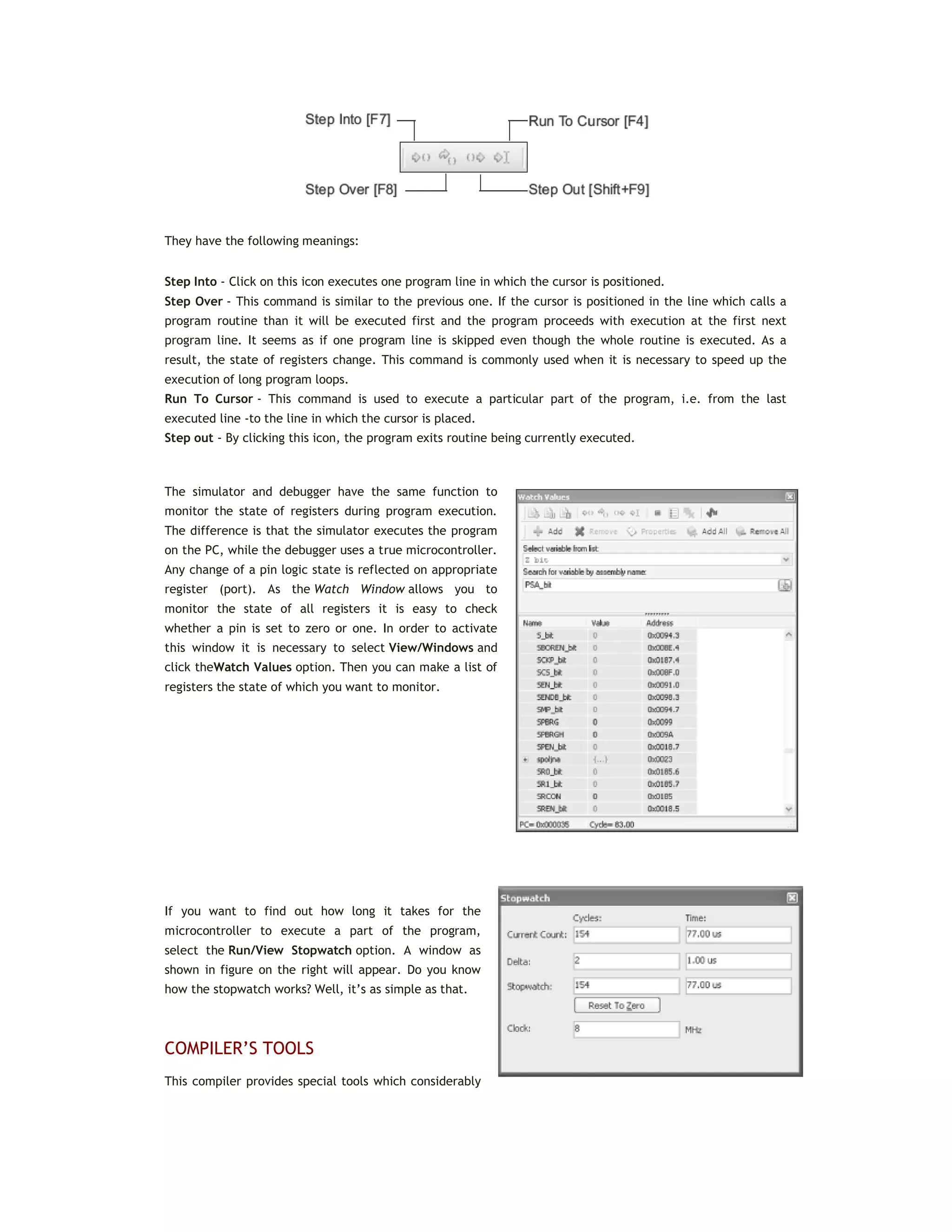
SOFTWARE SIMULATOR
Prior to starting up the simulator, select the appropriate mode in the Project
Settings Window (Build type - release) and click the Run /Start Debugger option.
The compiler will be automatically set in simulation mode. As such, it monitors
the state of all register bits. It also enables you to execute the program step by
step while monitoring the operation of the microcontroller on the screen (i.e.
simulation of operation).
A few icons, used only for the operation of this simulator, will be added to the
toolbar when setting the compiler in this mode.](https://image.slidesharecdn.com/fmwc6ltijaekc37-210710214315/75/Microcontroladores-Programacion-del-microcontrolador-PIC-en-C-56-2048.jpg)
![simplify the process of writing a program. All these tools are available from theTools menu. In the following
text we are going to give a brief description of all of them.
PICFLASH PROGRAMMER
PICflash programmer is a stand-alone program which can operate independently of the compiler, i.e. it can be
used as a separate program. However, in this case, its operation is closely related to the operation of the
compiler so that it can be activated from within the compiler itself. If installed, the PIC flash programmer is
activated by selecting Tools/me_Programmer or pressing [F11]. A window that appears contains options to be
used for the process of programming microcontrollers.
It’s the right time to explain the operation of the programmer. As you know, the compiler is a software which
compile the program written in a higher programming language into executable code, i.e. Hex code. That’s
the code the microcontroller understands and executes. The programmer, which loads this code into the chip,
is comprised of software and hardware together called - PICflash programmer. Programmer’s hardware
provides all necessary voltage levels and socket for placing the microcontroller in. Programmer’s software is
installed on the PC and is used to pass on the Hex code to hardware over USB cable. This book provides
discussion on the software only.
USART TERMINAL
The USART terminal is a replacement for the
standard Windows Hyper Terminal. It can be
used for checking the operation of the
microcontroller which uses USART
communication. Such a microcontroller is built in
a device and connected to the RS232 connector
on PC over serial cable. The USART terminal
window, shown on the right, contains options for
setting serial communication and for displaying
sent/received data.](https://image.slidesharecdn.com/fmwc6ltijaekc37-210710214315/75/Microcontroladores-Programacion-del-microcontrolador-PIC-en-C-58-2048.jpg)

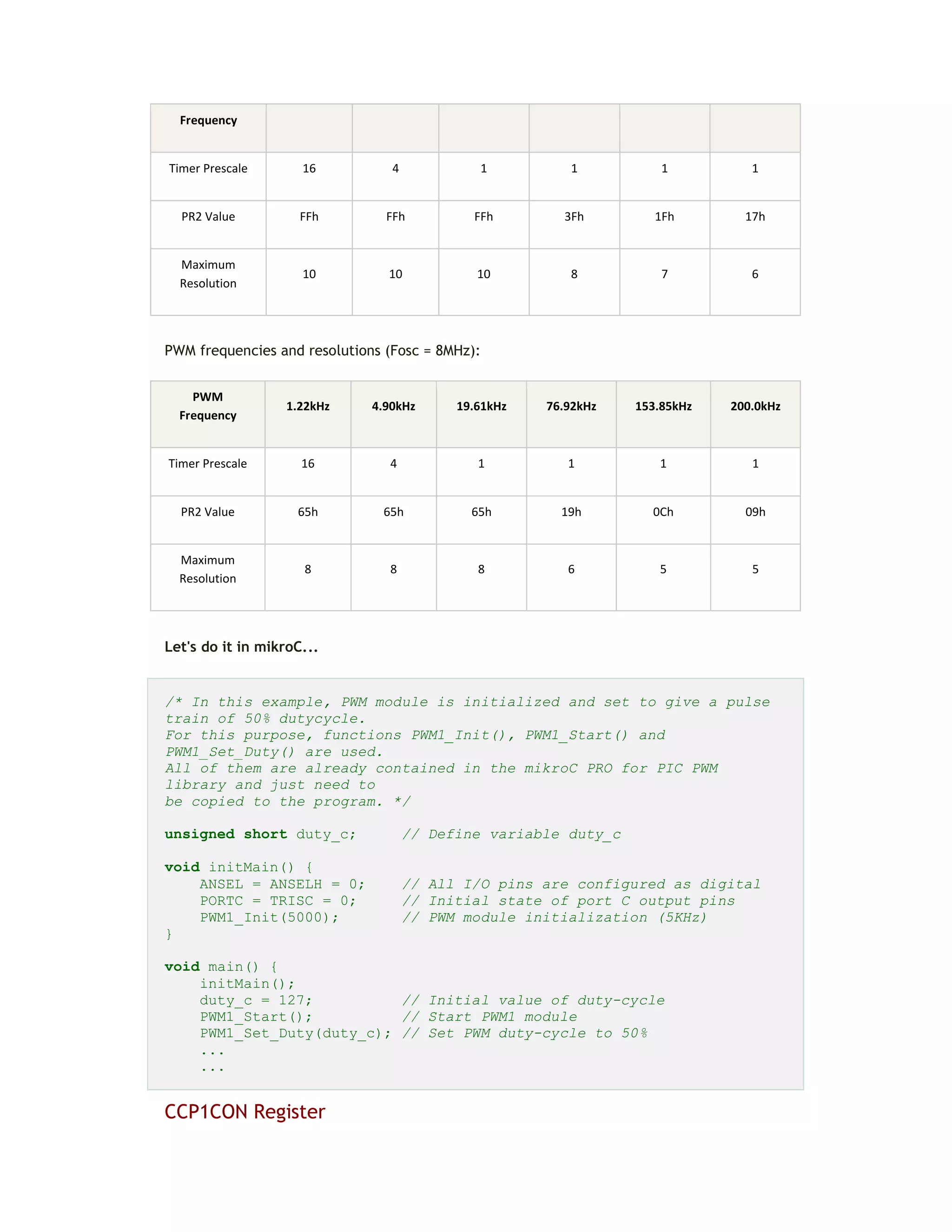
![The output pulse period (T) is determined by the PR2 register of the timer TMR2. The PWM
period can be calculated using the following equation:
PWM Period = (PR2 +1) * 4Tosc * TMR2 Prescale Value
If the PWM period (T) is known, then it is easy to determine the signal frequency F because
these two values are related by equation F=1/T.
PWM DUTY CYCLE
The PWM duty cycle is specified by using in total of 10 bits: eight MSbs of the CCPR1L register
and two additional LSbs of the CCP1CON register (DC1B1 and DC1B0). The result is a 10-bit
number contained in the formula:
Pulse Width = (CCPR1L,DC1B1,DC1B0) * Tosc * TMR2 Prescale Value
The following table shows how to generate PWM signals of varying frequency if the
microcontroller uses 20 MHz quartz-crystal (Tosc=50nS).
Frequency [KHz] 1.22 4.88 19.53 78.12 156.3 208.3
TMR2 Prescaler 16 4 1 1 1 1
PR2 Register FFh FFh FFh 3Fh 1Fh 17h
Just two more things:
The output pin will be constantly set if the pulse width is by negligence determined
to be larger than PWM period.
In this application, the timer TMR2 postscaler cannot be used for generation of longer
PWM periods.
PWM RESOLUTION
An PWM signal is nothing more than a pulse sequence with varying duty cycle. For one
specified frequency (number of pulses per second), there is a limited number of duty cycle
combinations. This number represents a resolution measured by bits. For example, a 10- bit
resolution will result in 1024 discrete duty cycles, whereas an 8-bit resolution will result in
256 discrete duty cycles etc. In relation to this microcontroller, the resolution is determined
by the PR2 register. The maximum value is obtained by writing number FFh.
PWM frequencies and resolutions (Fosc = 20MHz):
PWM
1.22kHz 4.88kHz 19.53kHz 78.12kHz 156.3kHz 208.3kHz](https://image.slidesharecdn.com/fmwc6ltijaekc37-210710214315/75/Microcontroladores-Programacion-del-microcontrolador-PIC-en-C-125-2048.jpg)

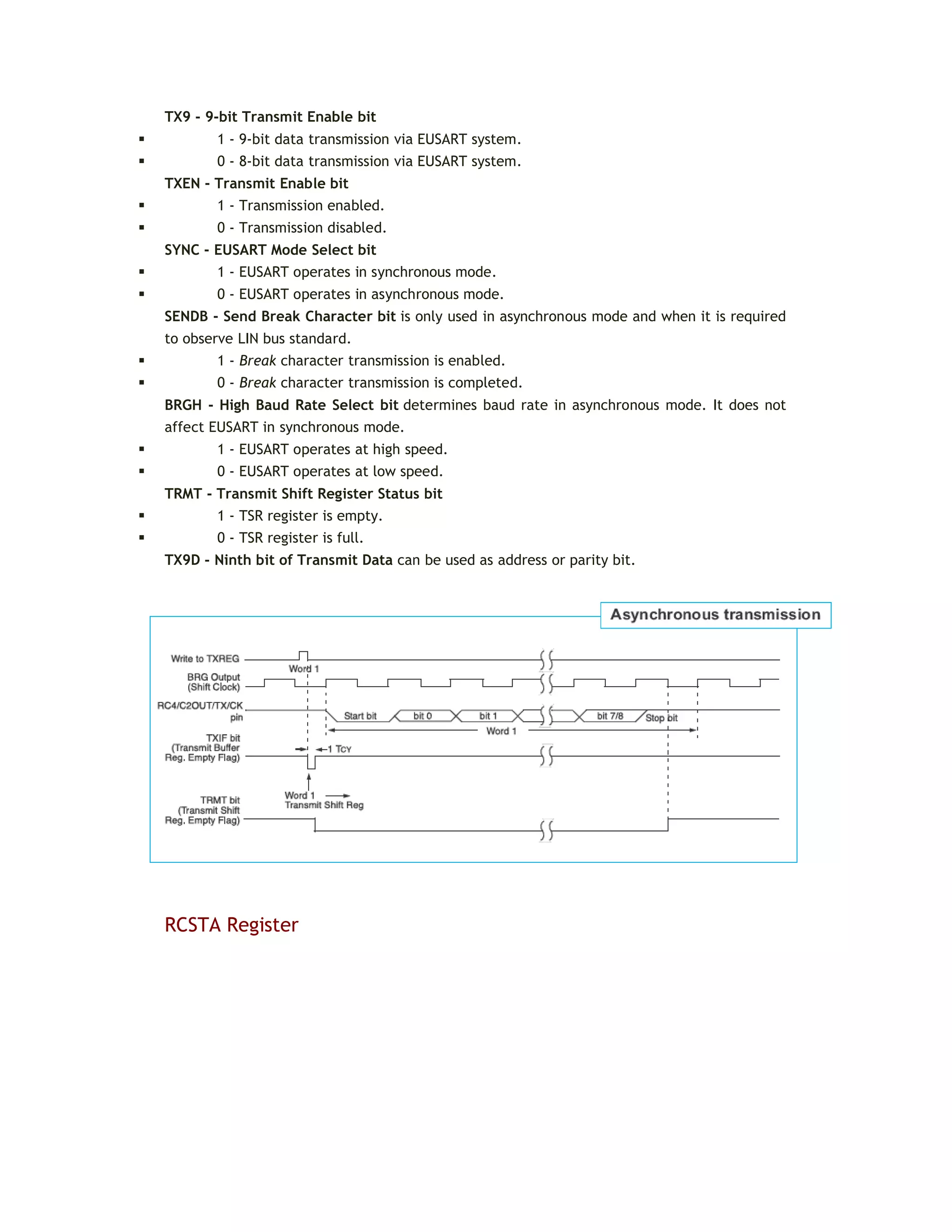
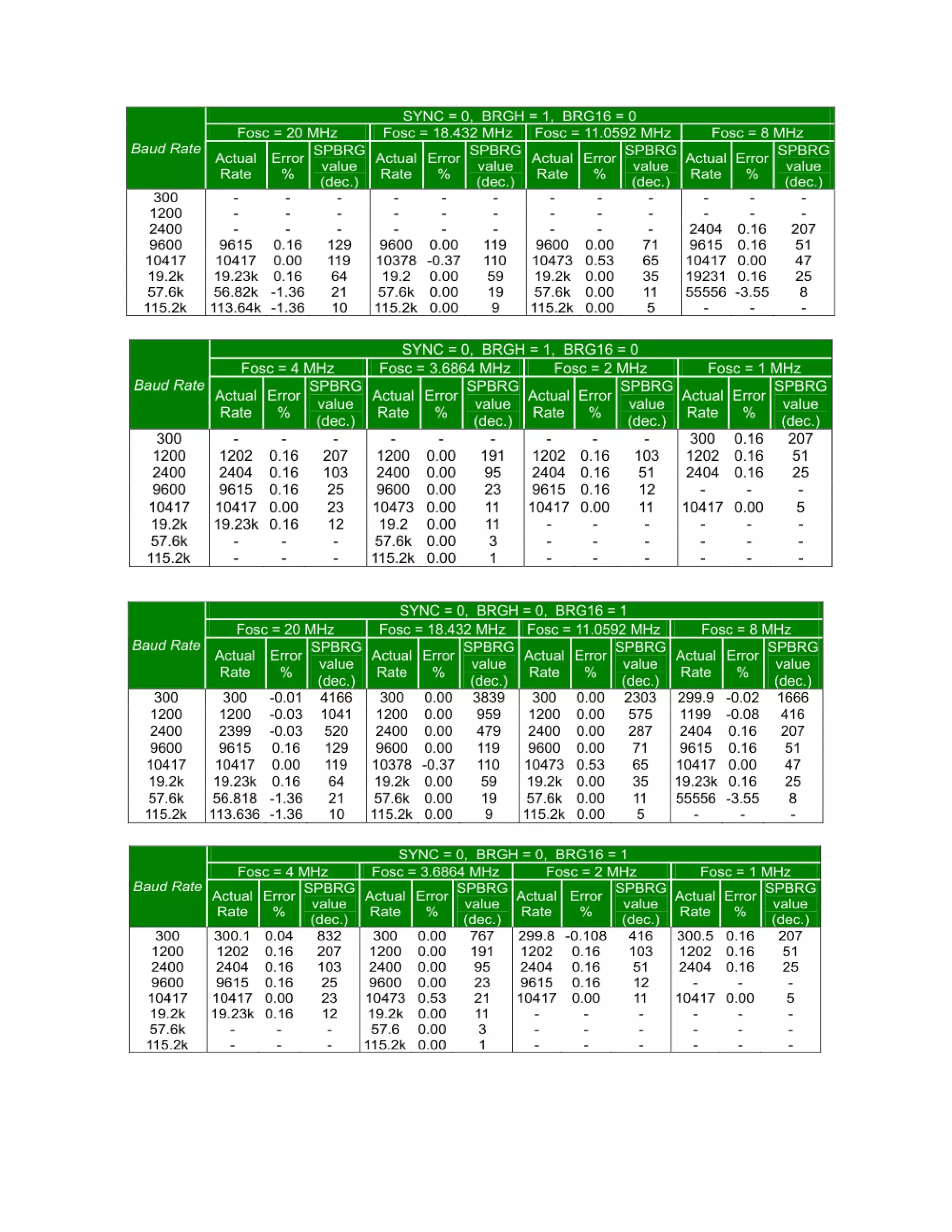
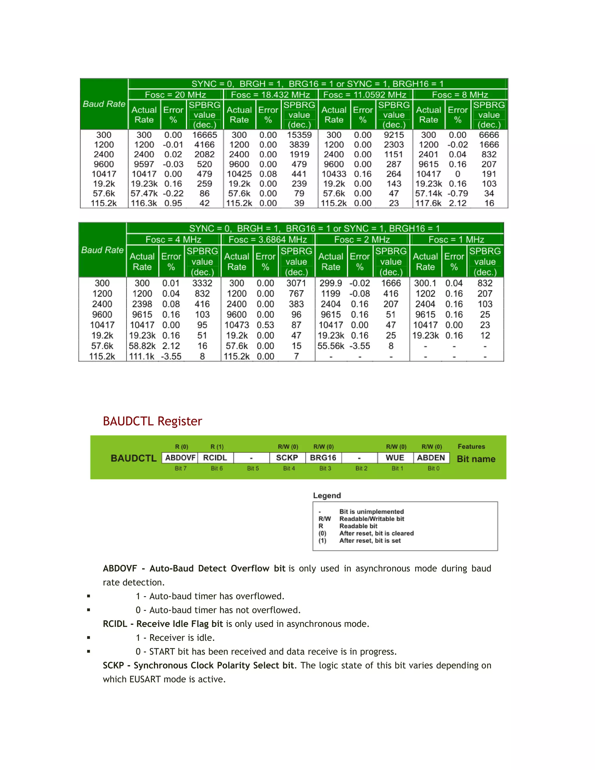
![EUSART BAUD RATE GENERATOR (BRG)
If you carefully look at asynchronous EUSART receiver or transmitter diagram, you will see
that both of them use clock signal from the local timer BRG for synchronization. The same
clock source is also used in synchronous mode.
The BRG timer consists of two 8-bit registers making one 16-bit register.
A number written to these two registers determines the baud rate. Besides, both the BRGH
bit of the TXSTAregister and the BRGH16 bit of the BAUDCTL register affect clock frequency.
The formula used to determine Baud Rate is given in the table below.
Bits
BRG / EUSART Mode Baud Rate Formula
SYNC BRG1G BRGH
0 0 0 8-bit / asynchronous Fosc / [64 (n + 1)]
0 0 1 8-bit / asynchronous Fosc / [16 (n + 1)]](https://image.slidesharecdn.com/fmwc6ltijaekc37-210710214315/75/Microcontroladores-Programacion-del-microcontrolador-PIC-en-C-148-2048.jpg)
![0 1 0 16-bit / asynchronous Fosc / [16 (n + 1)]
0 1 1 16-bit / asynchronous Fosc / [4 (n + 1)]
1 0 X 8-bit / asynchronous Fosc / [4 (n + 1)]
1 1 X 16-bit / asynchronous Fosc / [4 (n + 1)]
Tables on the following pages contain values that should be written to the 16-bit register
SPBRG and assigned to the SYNC, BRGH and BRGH16 bits in order to obtain some of the
standard baud rates. Use the following formulas to determine the Baud Rate:](https://image.slidesharecdn.com/fmwc6ltijaekc37-210710214315/75/Microcontroladores-Programacion-del-microcontrolador-PIC-en-C-149-2048.jpg)
![SSPM3-SSPM0 - Synchronous Serial Port Mode Select bits. SSP mode is determined by
combining these bits:
SSPCON2 Register
0 0 0 0 SPI master mode, clock = Fosc/4
0 0 0 1 SPI master mode, clock = Fosc/16
0 0 1 0 SPI master mode, clock = Fosc/64
0 0 1 1 SPI master mode, clock = (output TMR)/2
0 1 0 0 SPI slave mode, SS pin control enabled
0 1 0 1 SPI slave mode, SS pin control disabled, SS can be used as I/O pin
0 1 1 0 I²C slave mode, 7-bit address used
0 1 1 1 I²C slave mode, 10-bit address used
1 0 0 0 I²C master mode, clock = Fosc / [4(SSPAD+1)]
1 0 0 1 Mask used in I²C slave mode
1 0 1 0 Not used
1 0 1 1 I²C controlled master mode
1 1 0 0 Not used
1 1 0 1 Not used
1 1 1 0 I²C slave mode, 7-bit address used,START and STOP bits enable interrupt
1 1 1 1 I²C slave mode, 10-bit address used,START and STOP bits enable interrupt](https://image.slidesharecdn.com/fmwc6ltijaekc37-210710214315/75/Microcontroladores-Programacion-del-microcontrolador-PIC-en-C-163-2048.jpg)
![VREN Comparator C1 Voltage Reference Enable bit
1 - Voltage reference CVref source is powered on.
0 - Voltage reference CVref source is powered off.
VROE Comparator C2 Voltage Reference Enable bit
1 - Voltage reference CVref is connected to the pin.
0 - Voltage reference CVref is disconnected from the pin.
VRR - CVref Range Selection bit
1 - Voltage reference source is set to low range.
0 - Voltage reference source is set to high range.
VRSS - Comparator Vref Range selection bit
1 - Voltage reference source is in the range of Vref+ to Vref-.
0 - Voltage reference source is in the range of Vdd to Vss (power supply voltage).
VR3 - VR0 CVref Value Selection
If VRR = 1 (low range)
Voltage reference is calculated using the formula: CVref = ([VR3:VR0]/24)Vdd
If VRR = 0 (high range)
Voltage reference is calculated using the formula: CVref = Vdd/4 + ([VR3:VR0]/32)Vdds
In Short
In order to properly use built-in comparators, it is necessary to do the following:
Step 1 - Module Configuration:
In order to select the appropriate mode, bits of the CM1CON0 and CM2CON0 registers
should be configured. Interrupt should be disabled on any change of mode.
Step 2 - Internal voltage reference Vref source configuration (only when used). In the VRCON
register it is necessary to:
Select one of two voltage ranges using the VRR bit.
Configure necessary Vref using bits VR3 - VR0.
Set the VROE bit if needed.
Enable voltage Vref source by setting the VREN bit.
Formula used to calculate voltage reference:
VRR = 1 (low range)
CVref = ([VR3:VR0]/24)VLADDER
VRR = 0 (high range)
CVref = (VLADDER/4) + ([VR3:VR0]VLADDER/32)
Vladder = Vdd or ([Vref+] - [Vref-]) or Vref+
Step 3 - Start of operation:
Enable an interrupt by setting bits CMIE (PIE register), PEIE and GIE (INTCON register).](https://image.slidesharecdn.com/fmwc6ltijaekc37-210710214315/75/Microcontroladores-Programacion-del-microcontrolador-PIC-en-C-183-2048.jpg)
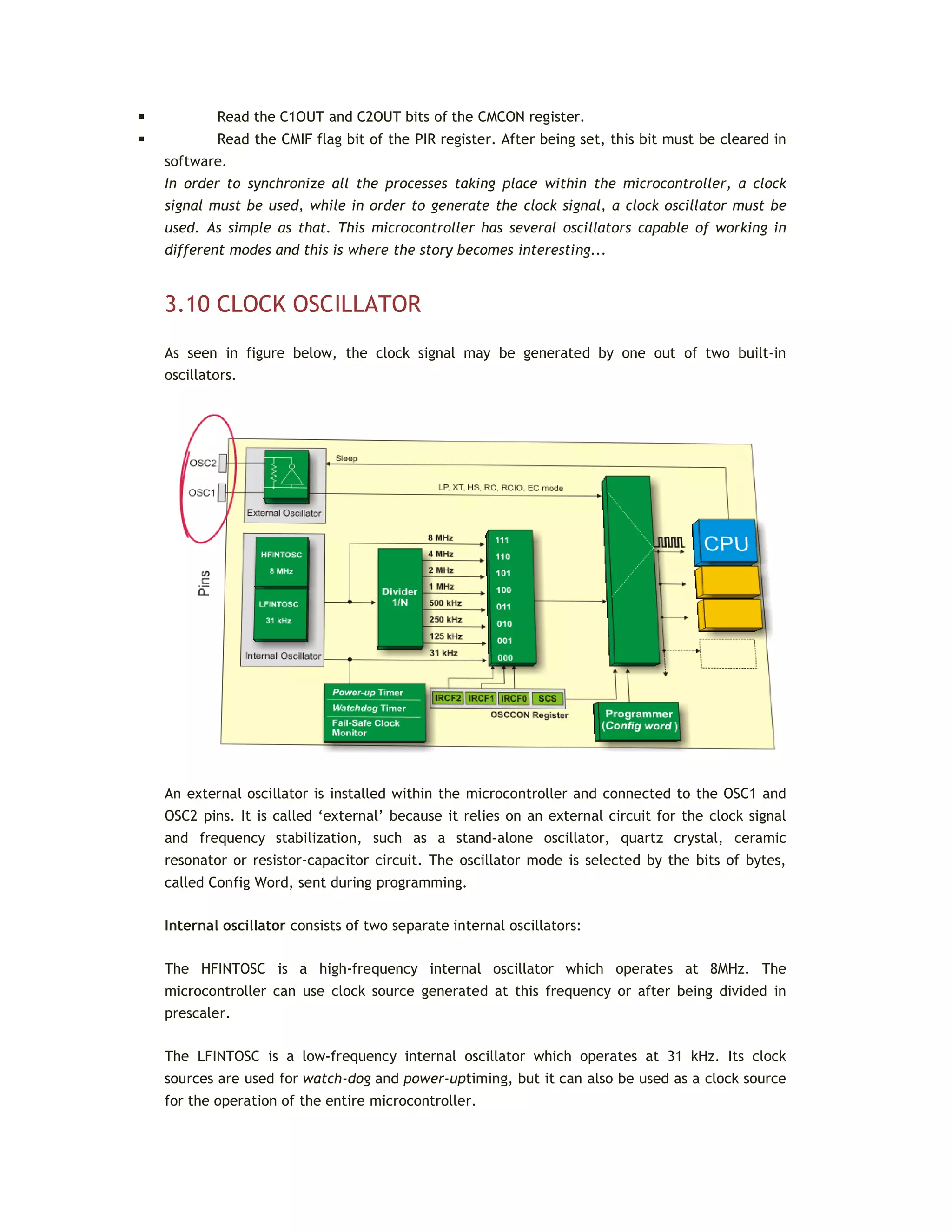
![EXTERNAL OSCILLATOR IN RC AND RCIO MODE
There are certainly many advantages in using elements for frequency stabilization, but
sometimes they are really unnecessary. In most cases the oscillator may operate at
frequencies not precisely defined so that embedding of such elements is a waste of money.
The simplest and cheapest solution in these situations is to use one resistor and one capacitor
for the operation of oscillator. There are two modes:
RC mode. When the external oscillator is
configured to operate in RC mode, the OSC1
pin should be connected to the RC circuit as
shown in figure on the right. The OSC2 pin
outputs the RC oscillator frequency divided by
4. This signal may be used for calibration,
synchronization or other application
requirements.
RCIO mode. Likewise, the RC circuit is
connected to the OSC1 pin. This time, the
available OSC2 pin is used as an additional
general-purpose I/O pin.
In both cases, it is recommended to use
components as shown in figure.
The frequency of such an oscillator is
calculated according to the formula f = 1/T in
which:
f = frequency [Hz];
T = R * C = time constant [s];
R = resistor resistance [Ω]; and
C = capacitor capacity [F].](https://image.slidesharecdn.com/fmwc6ltijaekc37-210710214315/75/Microcontroladores-Programacion-del-microcontrolador-PIC-en-C-189-2048.jpg)

![sbit LCD_EN at RB5_bit;
sbit LCD_D4 at RB0_bit;
sbit LCD_D5 at RB1_bit;
sbit LCD_D6 at RB2_bit;
sbit LCD_D7 at RB3_bit;
sbit LCD_RS_Direction at TRISB4_bit;
sbit LCD_EN_Direction at TRISB5_bit;
sbit LCD_D4_Direction at TRISB0_bit;
sbit LCD_D5_Direction at TRISB1_bit;
sbit LCD_D6_Direction at TRISB2_bit;
sbit LCD_D7_Direction at TRISB3_bit;
// End LCD module connections
const unsigned short TEMP_RESOLUTION = 9;
char *text = "000.0000";
unsigned temp;
void Display_Temperature(unsigned int temp2write) {
const unsigned short RES_SHIFT = TEMP_RESOLUTION - 8;
char temp_whole;
unsigned int temp_fraction;
// check if temperature is negative
if (temp2write & 0x8000) {
text[0] = '-';
temp2write = ~temp2write + 1;
}
// extract temp_whole
temp_whole = temp2write >> RES_SHIFT ;
// convert temp_whole to characters
if (temp_whole/100)
text[0] = temp_whole/100 + 48;
else
text[0] = '0';
text[1] = (temp_whole/10)%10 + 48; // Extract tens digit
text[2] = temp_whole%10 + 48; // Extract ones digit
// extract temp_fraction and convert it to unsigned int
temp_fraction = temp2write << (4-RES_SHIFT);
temp_fraction &= 0x000F;
temp_fraction *= 625;
// convert temp_fraction to characters
text[4] = temp_fraction/1000 + 48; // Extract thousands digit
text[5] = (temp_fraction/100)%10 + 48; // Extract hundreds digit
text[6] = (temp_fraction/10)%10 + 48; // Extract tens digit
text[7] = temp_fraction%10 + 48; // Extract ones digit
// Display temperature on LCD
Lcd_Out(2, 5, text);
}
void main() {
ANSEL = 0; // Configure AN pins as digital I/O
ANSELH = 0;
C1ON_bit = 0; // Disable comparators
C2ON_bit = 0;](https://image.slidesharecdn.com/fmwc6ltijaekc37-210710214315/75/Microcontroladores-Programacion-del-microcontrolador-PIC-en-C-249-2048.jpg)
![4.16 EXAMPLE 14
Using graphic LCD display
A graphic LCD (GLCD) provides an advanced method for displaying visual messages. While the
character LCD can display only alphanumeric characters, the GLCD can display messages in
the form of drawings and bitmaps. The most commonly used graphic LCD has 128x64 pixels
screen resolution. The GLCD contrast can be adjusted using the potentiometer P1.
Here, the GLCD displays a picture of truck the bitmap of which is stored in
the truck_bmp.c file.
/*Header******************************************************/
//Declarations--------------------------------------------------------
----------
const code char truck_bmp[1024];
//--------------------------------------------------------------end-
declarations
// Glcd module connections
char GLCD_DataPort at PORTD;
sbit GLCD_CS1 at RB0_bit;
sbit GLCD_CS2 at RB1_bit;
sbit GLCD_RS at RB2_bit;
sbit GLCD_RW at RB3_bit;
sbit GLCD_EN at RB4_bit;
sbit GLCD_RST at RB5_bit;
sbit GLCD_CS1_Direction at TRISB0_bit;
sbit GLCD_CS2_Direction at TRISB1_bit;
sbit GLCD_RS_Direction at TRISB2_bit;
sbit GLCD_RW_Direction at TRISB3_bit;
sbit GLCD_EN_Direction at TRISB4_bit;
sbit GLCD_RST_Direction at TRISB5_bit;](https://image.slidesharecdn.com/fmwc6ltijaekc37-210710214315/75/Microcontroladores-Programacion-del-microcontrolador-PIC-en-C-253-2048.jpg)
![#ifdef COMPLETE_EXAMPLE
Glcd_Fill(0xFF); // Fill GLCD
Glcd_Set_Font(Character8x7, 8, 7, 32); // Change font
someText = "8x7 Font";
Glcd_Write_Text(someText, 5, 0, 2); // Write string
delay2S();
Glcd_Set_Font(System3x5, 3, 5, 32); // Change font
someText = "3X5 CAPITALS ONLY";
Glcd_Write_Text(someText, 60, 2, 2); // Write string
delay2S();
Glcd_Set_Font(font5x7, 5, 7, 32); // Change font
someText = "5x7 Font";
Glcd_Write_Text(someText, 5, 4, 2); // Write string
delay2S();
Glcd_Set_Font(FontSystem5x7_v2, 5, 7, 32); // Change font
someText = "5x7 Font (v2)";
Glcd_Write_Text(someText, 5, 6, 2); // Write string
delay2S();
#endif
}
}
truck_bmp.c file:
/*Header******************************************************/
unsigned char const truck_bmp[1024] = {
0,0,0,0,0,248,8,8,8,8,8,8,12,12,12,12,12,10,10,10,10,10,10,9,9,9,9,9,9
,9,9,9,9,9
,9,9,9,9,9,9,9,9,137,137,137,137,137,137,137,137,137,137,137,137,137,9
,9,9,9,9,9
,9,9,9,9,9,13,253,13,195,6,252,0,0,0,0,0,0,0,0,0,0,0,0,0,0,0,0,0,0,0,0
,0,0,0,0,0
,0,0,0,0,0,0,0,0,0,0,0,0,0,0,0,0,0,0,0,0,0,0,0,0,0,0,0,0,0,0,0,0,0,0,0
,0,255,0,0
,0,0,0,0,0,0,0,0,240,240,240,240,240,224,224,240,240,240,240,240,224,1
92,192,224
,240,240,240,240,240,224,192,0,0,0,255,255,255,255,255,195,195,195,195
,195,195,1
95,3,0,0,0,0,0,0,0,0,0,0,0,0,255,240,79,224,255,96,96,96,32,32,32,32,3
2,32,32,32
,32,32,32,32,32,64,64,64,64,128,0,0,0,0,0,0,0,0,0,0,0,0,0,0,0,0,0,0,0,
0,0,0,0,0,
0,0,0,0,0,0,0,0,0,0,0,0,0,0,0,0,255,0,0,0,0,0,0,0,0,0,0,255,255,255,25
5,255,0,0,
0,0,255,255,255,255,255,0,0,0,0,255,255,255,255,255,0,0,0,255,255,255,
255,255,12
9,129,129,129,129,129,129,128,0,0,0,0,0,0,0,0,0,0,0,0,255,1,248,8,8,8,
8,8,8,8,8,
8,8,8,8,8,816,224,24,36,196,70,130,130,133,217,102,112,160,192,96,96,3
2,32,160,1
60,224,224,192,64,64,128,128,192,64,128,0,0,0,0,0,0,0,0,0,0,0,0,0,0,0,
0,0,0,0,63](https://image.slidesharecdn.com/fmwc6ltijaekc37-210710214315/75/Microcontroladores-Programacion-del-microcontrolador-PIC-en-C-255-2048.jpg)
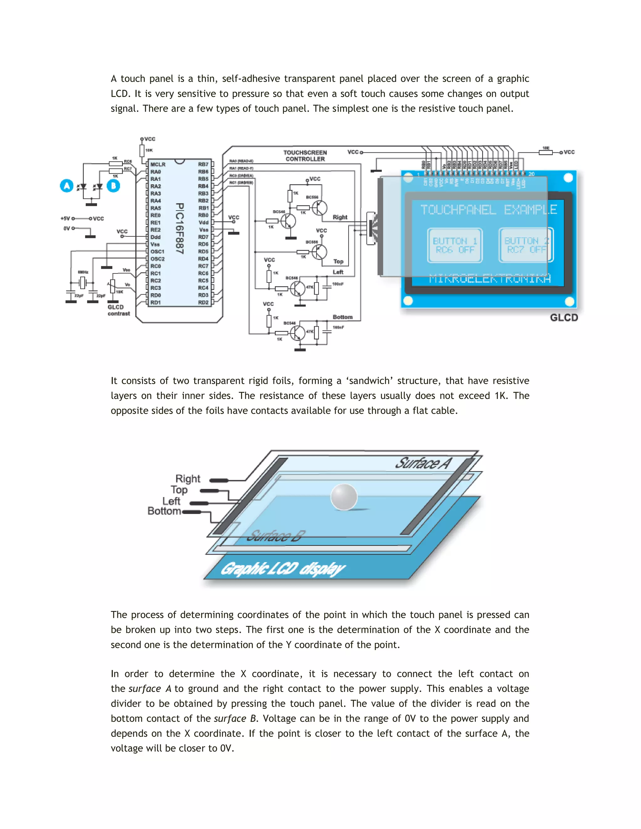
![In order to determine the Y coordinate, it is necessary to connect the bottom contact on
the surface B to ground, and the upper contact to power supply. In this case, the voltage is
read on the left contact of the surface A.
In order to connect a touch panel to the microcontroller it is necessary to create a circuit for
touch panel control. By means of this circuit, the microcontroller connects appropriate
contacts of the touch panel to ground and the power supply (as described above) in order to
determine the X and Y coordinates. The bottom contact of the surface B and left contact of
the surface A are connected to the microcontroller’s A/D converter. The X and Y coordinates
are determined by measuring voltage on these contacts, respectively. The software consists
of writing a menu on graphic LCD, turning the circuit for touch panel control on/off (driving
touch panel) and reading the values of A/D converter which actually represent the X and Y
coordinates of the point.
Once the coordinates are determined, it is possible to decide what we want the
microcontroller to do. In this example, microcontroller turns on/off two digital pins,
connected to LED diodes A and B.
This example use functions belonging to the Glcd and ADC library.
Considering that the touch panel surface is slightly larger than the surface of the graphic
LCD, in case you want greater accuracy when determining the coordinates, it is necessary to
perform the software calibration of the touch panel.
const char msg1[] = "TOUCHPANEL EXAMPLE";
const char msg2[] = "MIKROELEKTRONIKA";
const char msg3[] = "BUTTON1";
const char msg4[] = "BUTTON2";
const char msg5[] = "RC6 OFF";
const char msg6[] = "RC7 OFF";
const char msg7[] = "RC6 ON ";
const char msg8[] = "RC7 ON ";
long x_coord, y_coord, x_coord128, y_coord64; // scaled x-y position
char msg[16];
char * CopyConst2Ram(char * dest, const char * src){
for(;*dest++ = *src++;)
;
return dest;
}
// Glcd module connections
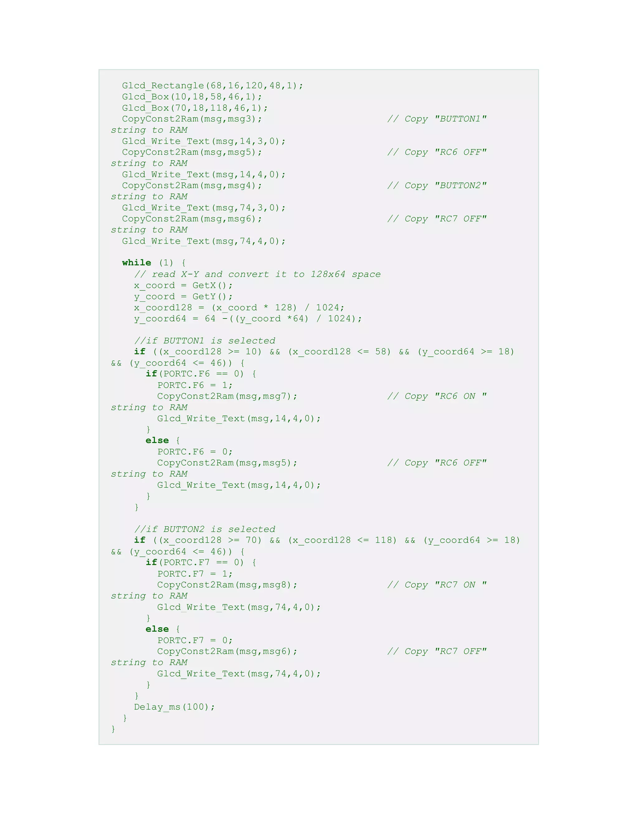
char GLCD_DataPort at PORTD;](https://image.slidesharecdn.com/fmwc6ltijaekc37-210710214315/75/Microcontroladores-Programacion-del-microcontrolador-PIC-en-C-258-2048.jpg)


This document provides an overview of different number systems including binary, decimal, and hexadecimal. It discusses how binary numbers are used in digital electronics and computers due to their simplicity of representing on/off states. Hexadecimal is presented as a base-16 system that uses 16 symbols to represent values in a more human-readable way compared to binary. Conversion between number systems such as binary to decimal and hexadecimal to binary is also covered. Key terms like bit, byte, and prefixes/suffixes for marking number systems are defined to clarify their meanings and avoid confusion.