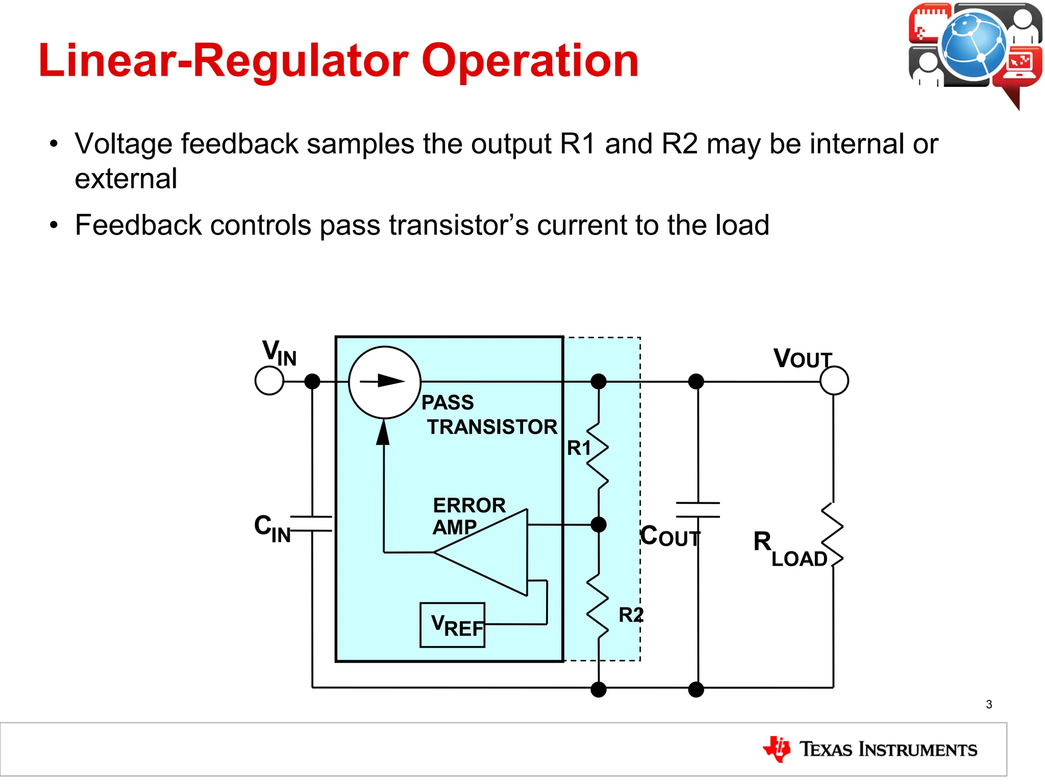
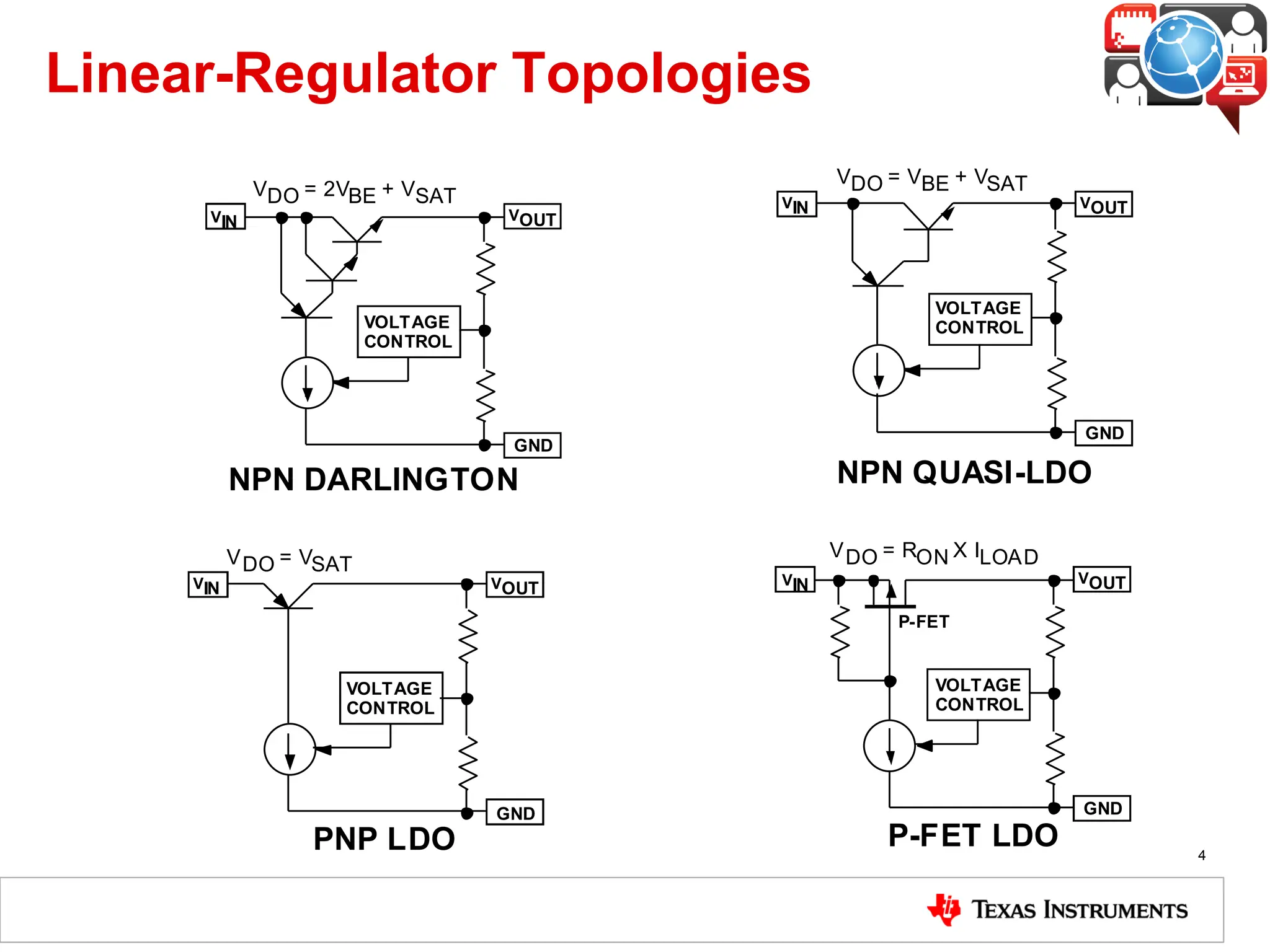
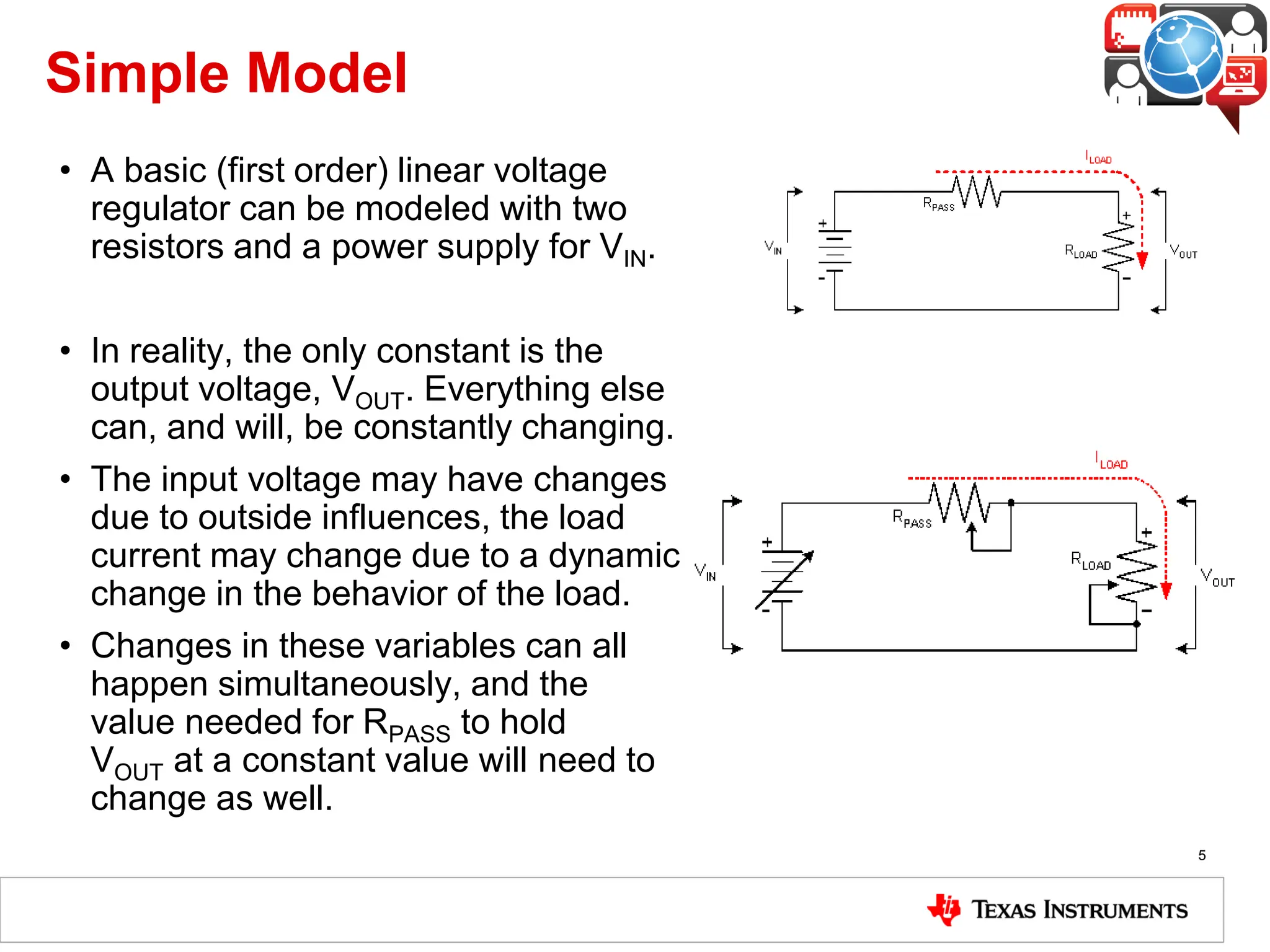
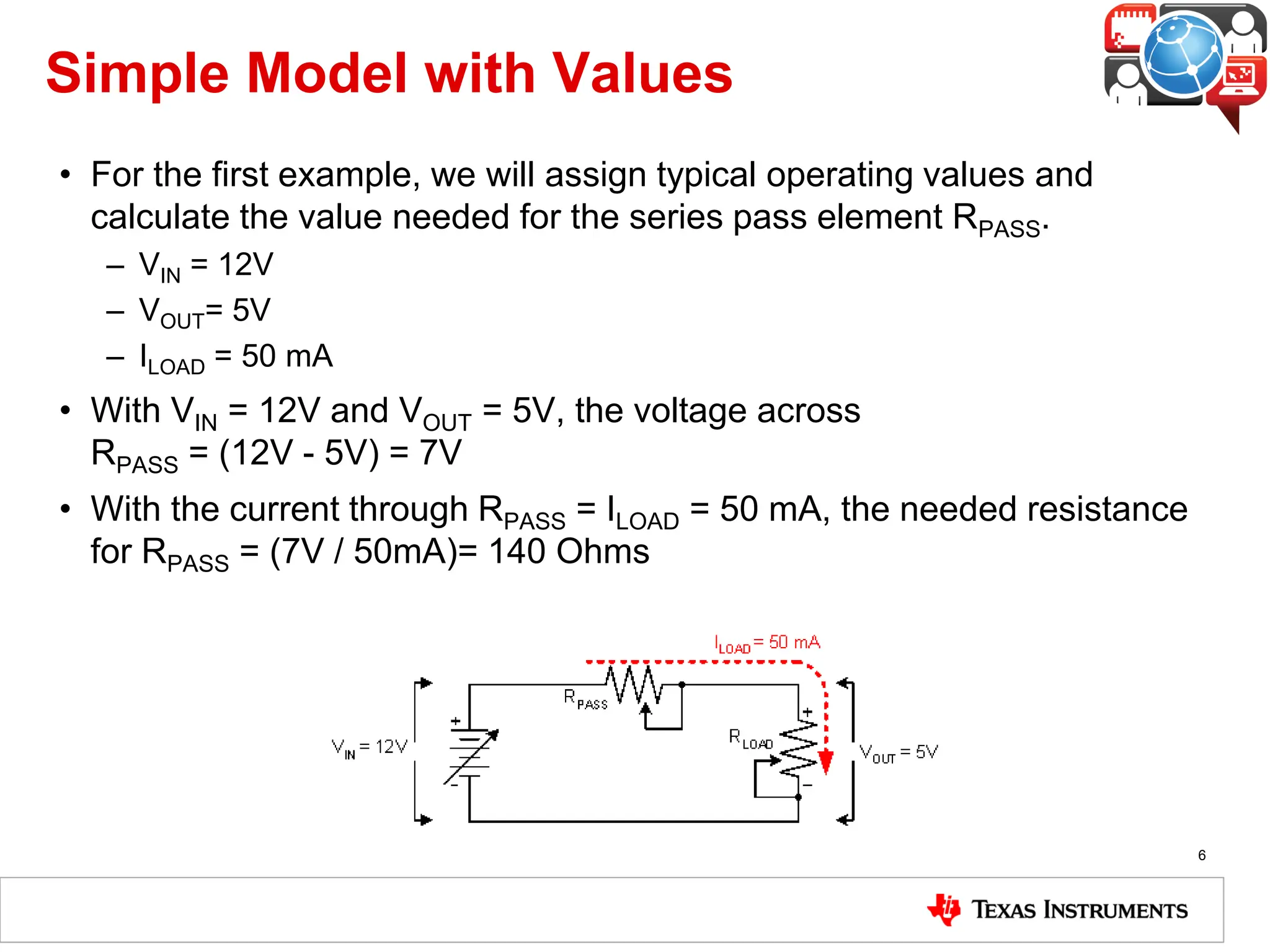
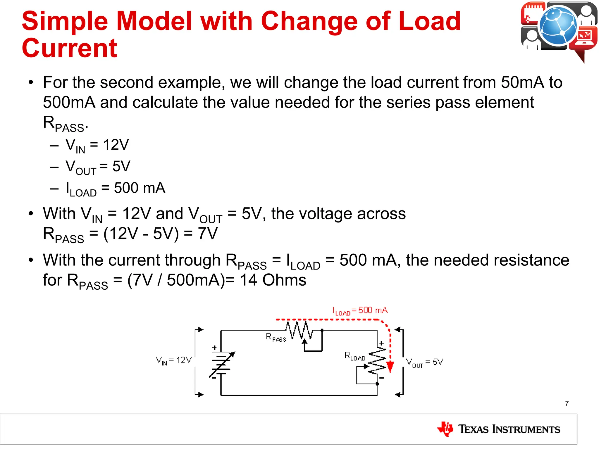
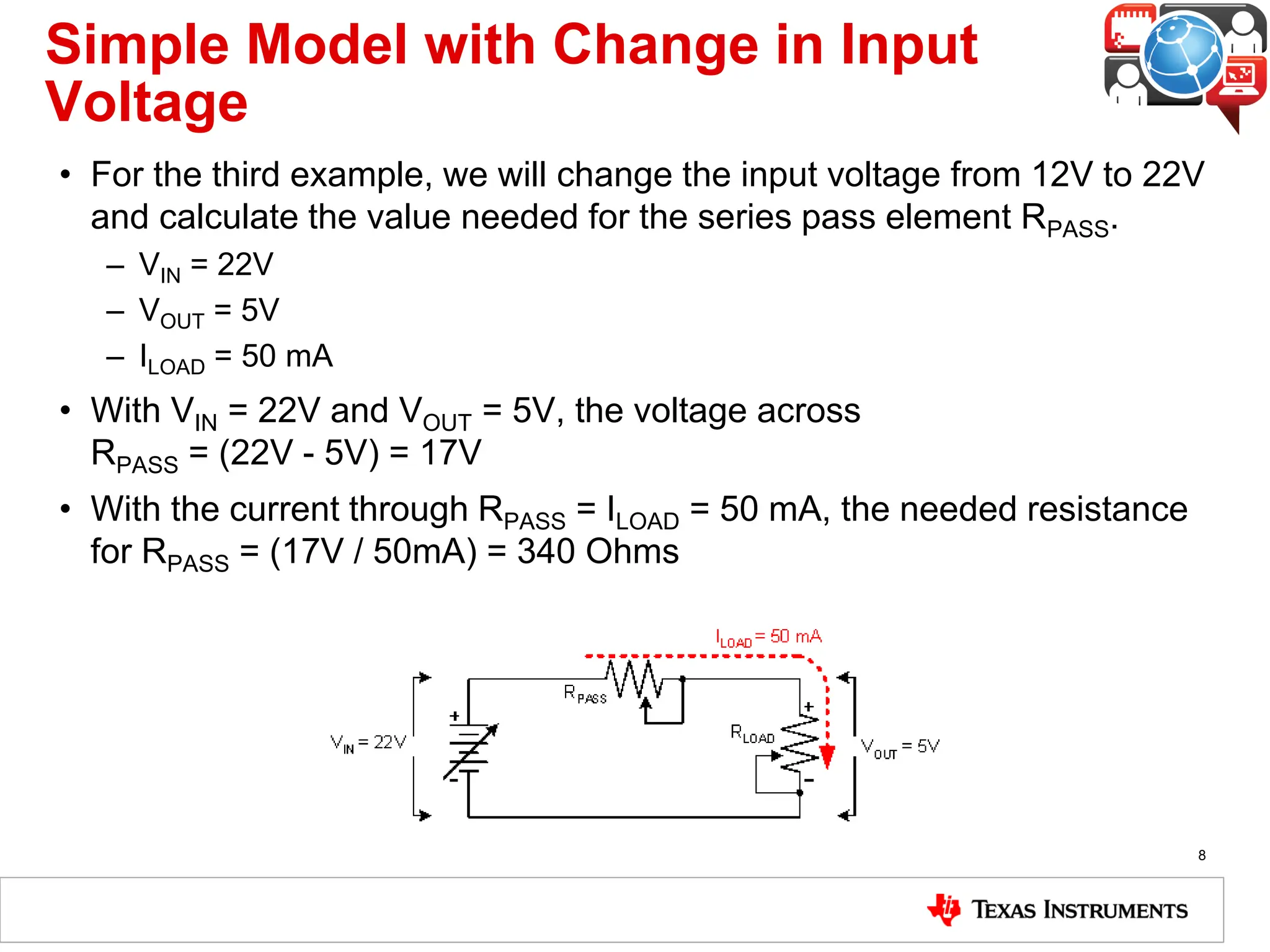
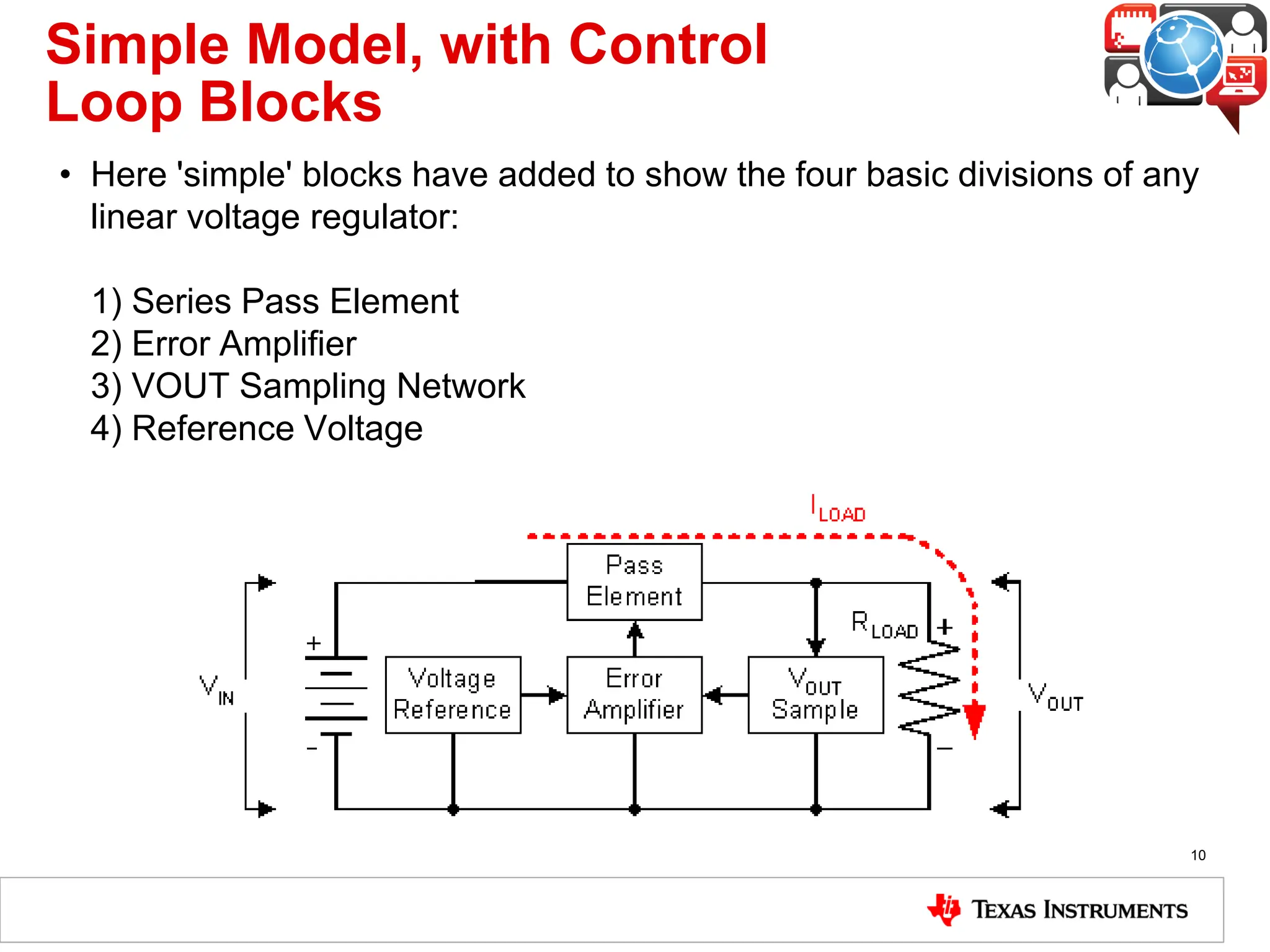
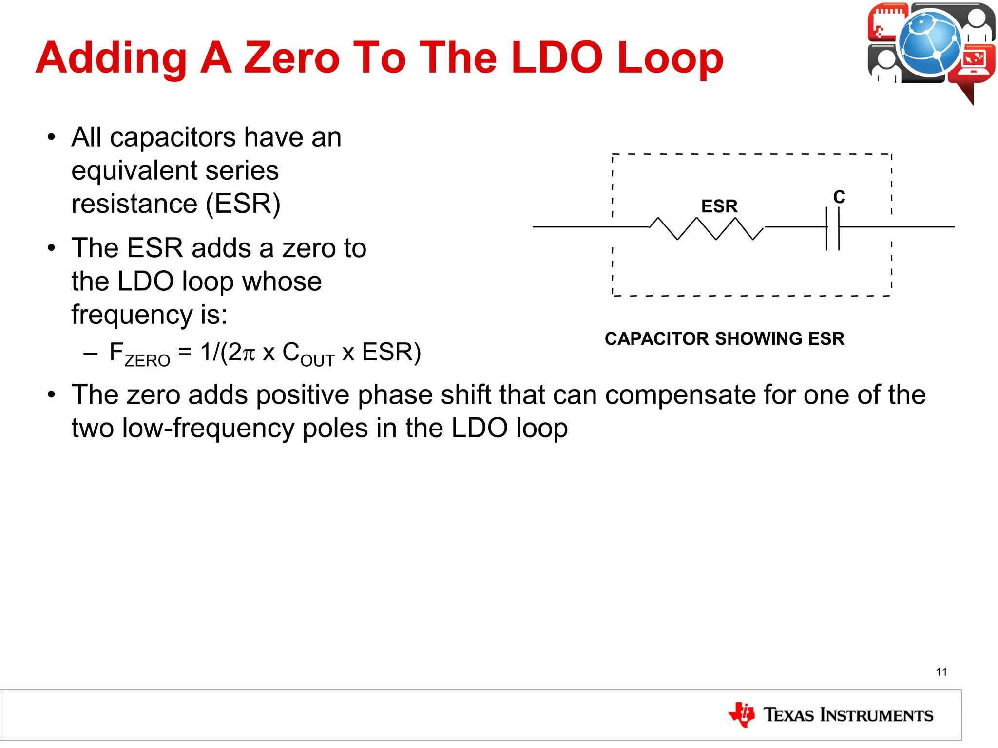
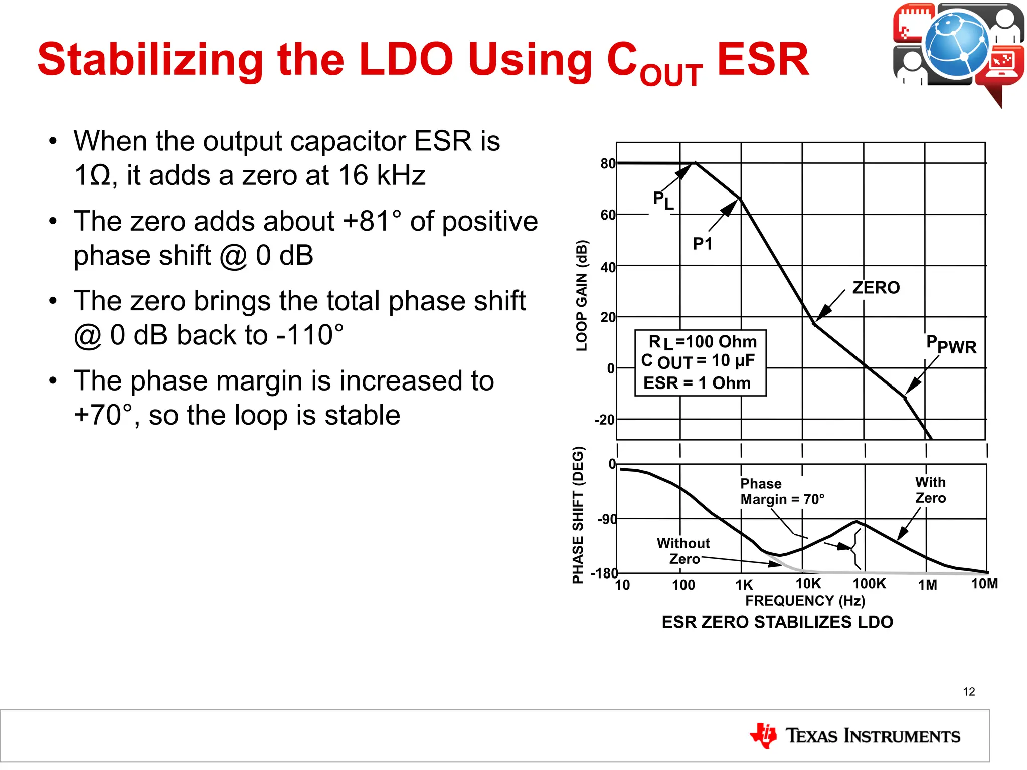
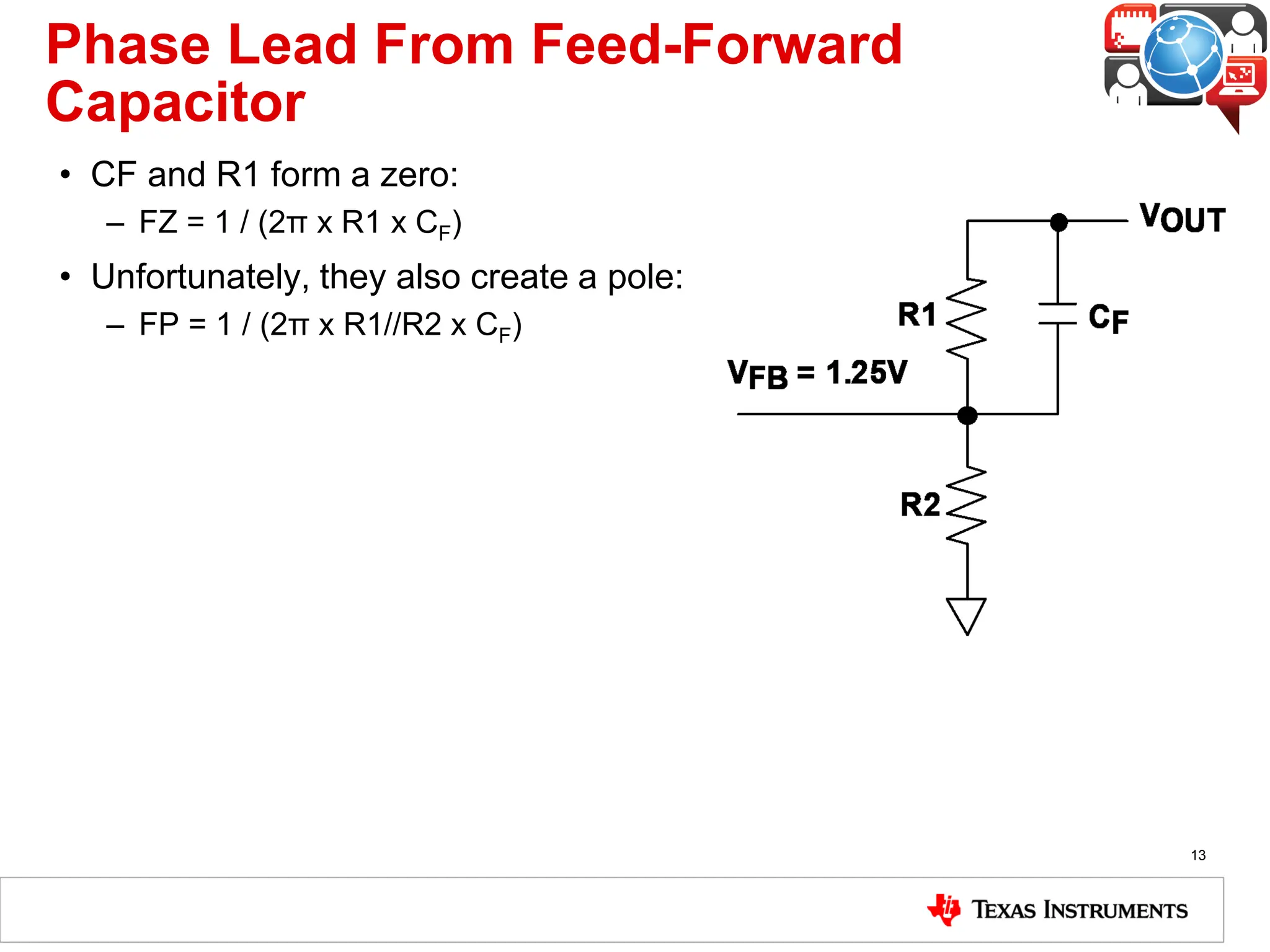
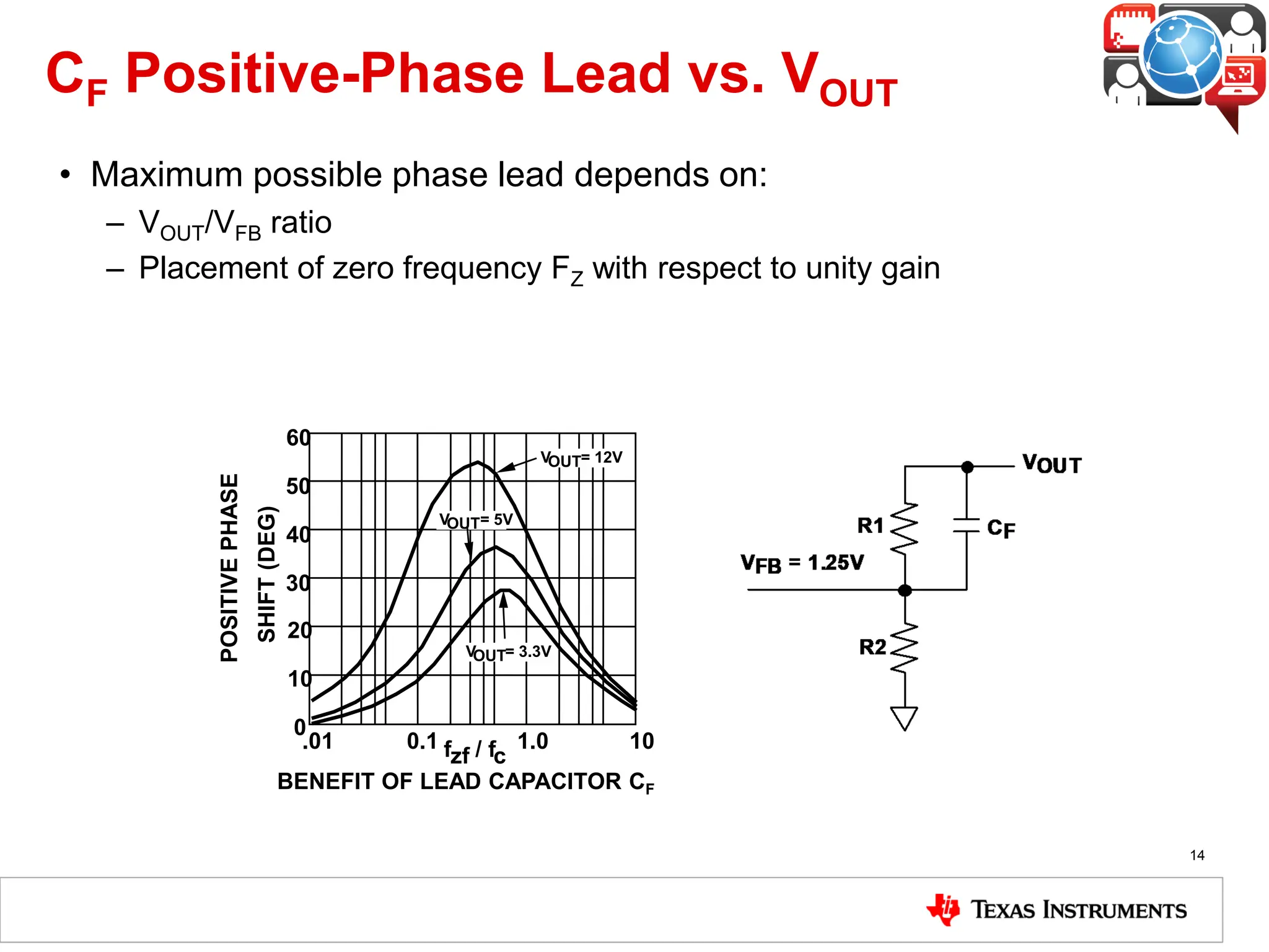
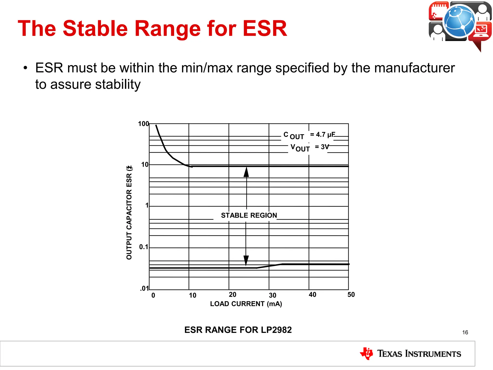
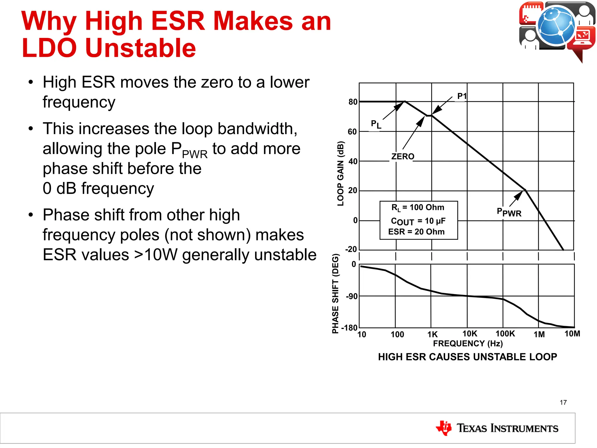
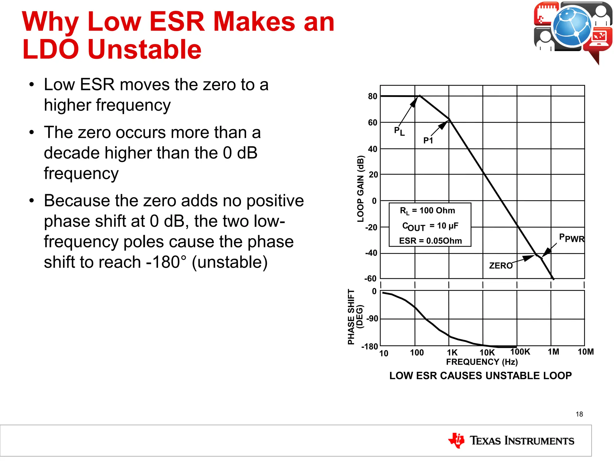
Linear Regulator Fundamentals
2.1 Types of Linear Regulators
What is a Linear Voltage Regulator
• A linear regulator operates by using a voltage-controlled current source
to force a fixed voltage to appear at the regulator output terminal. The
control circuitry continuously monitors (senses) the output voltage, and
adjusts the current source (as required by the load) to hold the output
voltage at the desired value.
• The design limit of the current source defines the maximum load
current the regulator can source and still maintain regulation.
• The output voltage is controlled using a feedback loop, which requires
some type of compensation to assure loop stability. Most linear
regulators have built-in compensation, and are completely stable
without external components.
• Some regulators (like Low-Dropout types), do require some external
capacitance connected from the output lead to ground to assure
regulator stability.
2
Linear-Regulator Operation
• Voltage feedback samples the output R1 and R2 may be internal or
external
• Feedback controls pass transistor’s current to the load
3
VIN
VREF
CIN
VOUT
COUT R
LOAD
ERROR
AMP
PASS
TRANSISTOR
R1
R2
Linear-Regulator Topologies
VIN VOUT
GND
VOLTAGE
CONTROL
P-FET
VIN VOUT
GND
VOLTAGE
CONTROL
NPN DARLINGTON
VIN VOUT
GND
VOLTAGE
CONTROL
PNP LDO
VIN VOUT
GND
VOLTAGE
CONTROL
NPN QUASI-LDO
P-FET LDO
VDO = 2VBE + VSAT
VDO = VBE + VSAT
VDO = VSAT
VDO = RON X ILOAD
4
Simple Model
• A basic (first order) linear voltage
regulator can be modeled with two
resistors and a power supply for VIN.
• In reality, the only constant is the
output voltage, VOUT. Everything else
can, and will, be constantly changing.
• The input voltage may have changes
due to outside influences, the load
current may change due to a dynamic
change in the behavior of the load.
• Changes in these variables can all
happen simultaneously, and the
value needed for RPASS to hold
VOUT at a constant value will need to
change as well.
5
Simple Model with Values
• For the first example, we will assign typical operating values and
calculate the value needed for the series pass element RPASS.
– VIN = 12V
– VOUT= 5V
– ILOAD = 50 mA
• With VIN = 12V and VOUT = 5V, the voltage across
RPASS = (12V - 5V) = 7V
• With the current through RPASS = ILOAD = 50 mA, the needed resistance
for RPASS = (7V / 50mA)= 140 Ohms
6
Simple Model with Change of Load
Current
• For the second example, we will change the load current from 50mA to
500mA and calculate the value needed for the series pass element
RPASS.
– VIN = 12V
– VOUT = 5V
– ILOAD = 500 mA
• With VIN = 12V and VOUT = 5V, the voltage across
RPASS = (12V - 5V) = 7V
• With the current through RPASS = ILOAD = 500 mA, the needed resistance
for RPASS = (7V / 500mA)= 14 Ohms
7
Simple Model with Change in Input
Voltage
• For the third example, we will change the input voltage from 12V to 22V
and calculate the value needed for the series pass element RPASS.
– VIN = 22V
– VOUT = 5V
– ILOAD = 50 mA
• With VIN = 22V and VOUT = 5V, the voltage across
RPASS = (22V - 5V) = 17V
• With the current through RPASS = ILOAD = 50 mA, the needed resistance
for RPASS = (17V / 50mA) = 340 Ohms
8
The Control Loop
• It has been shown that the resistance of series pass element, RPASS,
needs to change as the operating conditions change.
• This is accomplished with a control loop.
• The error amplifier monitors the sampled output voltage, compares it to
a known reference voltage, and actively changes RPASS to keep
VOUT constant.
– A characteristic of any linear voltage regulator is that it requires a finite
amount of time to "correct" the output voltage after a change in load current
demand.
– This "time lag" defines the characteristic called transient response, which is
a measure of how fast the regulator returns to steady-state conditions after
a load change
9
Simple Model, with Control
Loop Blocks
• Here 'simple' blocks have added to show the four basic divisions of any
linear voltage regulator:
1) Series Pass Element
2) Error Amplifier
3) VOUT Sampling Network
4) Reference Voltage
10
Adding A Zero To The LDO Loop
• All capacitors have an
equivalent series
resistance (ESR)
• The ESR adds a zero to
the LDO loop whose
frequency is:
– FZERO = 1/(2 x COUT x ESR)
• The zero adds positive phase shift that can compensate for one of the
two low-frequency poles in the LDO loop
CAPACITOR SHOWING ESR
ESR
C
11
Stabilizing the LDO Using COUT ESR
• When the output capacitor ESR is
1Ω, it adds a zero at 16 kHz
• The zero adds about +81° of positive
phase shift @ 0 dB
• The zero brings the total phase shift
@ 0 dB back to -110°
• The phase margin is increased to
+70°, so the loop is stable -20
0
20
40
60
80
LOOP
GAIN
(dB)
PL
P1
PPWR
ZERO
ESR = 1 Ohm
C = 10 µF
OUT
R =100 Ohm
L
ESR ZERO STABILIZES LDO
10 100 1K 10K 100K 1M 10M
FREQUENCY (Hz)
0
-90
-180
PHASE
SHIFT
(DEG)
Phase
Margin = 70°
Without
Zero
With
Zero
12
Phase Lead From Feed-Forward
Capacitor
• CF and R1 form a zero:
– FZ = 1 / (2π x R1 x CF)
• Unfortunately, they also create a pole:
– FP = 1 / (2π x R1//R2 x CF)
13
CF Positive-Phase Lead vs. VOUT
• Maximum possible phase lead depends on:
– VOUT/VFB ratio
– Placement of zero frequency FZ with respect to unity gain
0
20
40
60
.01 0.1 1.0 10
fzf / fc
POSITIVE
PHASE
SHIFT
(DEG)
10
30
50
V
OUT= 12V
V
OUT= 5V
V
OUT= 3.3V
BENEFIT OF LEAD CAPACITOR CF
14
De-Stabilizing the LDO Loop:
How to Build an Oscillator
• What is the most common reason why an LDO oscillates? THE
OUTPUT CAPACITOR!
– 1. ESR too high
• Poor quality tantalum capacitors can have a high ESR
• An aluminum electrolytic will have a high ESR at cold temperatures
– 2. ESR too low
• Many surface-mount ceramic capacitors have very low (<20 mW) ESRs
• Tantalum, OSCON, SP, POSCAP, film capacitors all have low ESRs
15
The Stable Range for ESR
• ESR must be within the min/max range specified by the manufacturer
to assure stability
16
LOAD CURRENT (mA)
OUTPUT
CAPACITOR
ESR
(ž
)
0 10 20 30 40 50
.01
0.1
1
10
100
C OUT = 4.7 µF
STABLE REGION
VOUT = 3V
ESR RANGE FOR LP2982
Why High ESR Makes an
LDO Unstable
• High ESR moves the zero to a lower
frequency
• This increases the loop bandwidth,
allowing the pole PPWR to add more
phase shift before the
0 dB frequency
• Phase shift from other high
frequency poles (not shown) makes
ESR values >10W generally unstable
17
-20
0
20
40
60
80
LOOP
GAIN
(dB)
PL
P1
PPWR
ZERO
ESR = 20 Ohm
C = 10 µF
OUT
10 100 1K 10K 100K 1M 10M
FREQUENCY (Hz)
0
-90
-180
PHASE
SHIFT
(DEG)
HIGH ESR CAUSES UNSTABLE LOOP
RL = 100 Ohm
Why Low ESR Makes an
LDO Unstable
• Low ESR moves the zero to a
higher frequency
• The zero occurs more than a
decade higher than the 0 dB
frequency
• Because the zero adds no positive
phase shift at 0 dB, the two low-
frequency poles cause the phase
shift to reach -180° (unstable)
18
-20
0
20
40
60
80
LOOP
GAIN
(dB)
PL
P1
ZERO
-40
-60
LOW ESR CAUSES UNSTABLE LOOP
10 100 1K 10K 100K 1M 10M
FREQUENCY (Hz)
0
-90
-180
PHASE
SHIFT
(DEG)
OUT
ESR = 0.05Ohm
C = 10 µF
PPWR
RL = 100 Ohm
Thank you!
19

linear-regulator-fundamentals-types-of-linear-regulators-presentation.pdf

  • 1.
    Linear Regulator Fundamentals 2.1Types of Linear Regulators
  • 2.
    What is aLinear Voltage Regulator • A linear regulator operates by using a voltage-controlled current source to force a fixed voltage to appear at the regulator output terminal. The control circuitry continuously monitors (senses) the output voltage, and adjusts the current source (as required by the load) to hold the output voltage at the desired value. • The design limit of the current source defines the maximum load current the regulator can source and still maintain regulation. • The output voltage is controlled using a feedback loop, which requires some type of compensation to assure loop stability. Most linear regulators have built-in compensation, and are completely stable without external components. • Some regulators (like Low-Dropout types), do require some external capacitance connected from the output lead to ground to assure regulator stability. 2
  • 3.
    Linear-Regulator Operation • Voltagefeedback samples the output R1 and R2 may be internal or external • Feedback controls pass transistor’s current to the load 3 VIN VREF CIN VOUT COUT R LOAD ERROR AMP PASS TRANSISTOR R1 R2
  • 4.
    Linear-Regulator Topologies VIN VOUT GND VOLTAGE CONTROL P-FET VINVOUT GND VOLTAGE CONTROL NPN DARLINGTON VIN VOUT GND VOLTAGE CONTROL PNP LDO VIN VOUT GND VOLTAGE CONTROL NPN QUASI-LDO P-FET LDO VDO = 2VBE + VSAT VDO = VBE + VSAT VDO = VSAT VDO = RON X ILOAD 4
  • 5.
    Simple Model • Abasic (first order) linear voltage regulator can be modeled with two resistors and a power supply for VIN. • In reality, the only constant is the output voltage, VOUT. Everything else can, and will, be constantly changing. • The input voltage may have changes due to outside influences, the load current may change due to a dynamic change in the behavior of the load. • Changes in these variables can all happen simultaneously, and the value needed for RPASS to hold VOUT at a constant value will need to change as well. 5
  • 6.
    Simple Model withValues • For the first example, we will assign typical operating values and calculate the value needed for the series pass element RPASS. – VIN = 12V – VOUT= 5V – ILOAD = 50 mA • With VIN = 12V and VOUT = 5V, the voltage across RPASS = (12V - 5V) = 7V • With the current through RPASS = ILOAD = 50 mA, the needed resistance for RPASS = (7V / 50mA)= 140 Ohms 6
  • 7.
    Simple Model withChange of Load Current • For the second example, we will change the load current from 50mA to 500mA and calculate the value needed for the series pass element RPASS. – VIN = 12V – VOUT = 5V – ILOAD = 500 mA • With VIN = 12V and VOUT = 5V, the voltage across RPASS = (12V - 5V) = 7V • With the current through RPASS = ILOAD = 500 mA, the needed resistance for RPASS = (7V / 500mA)= 14 Ohms 7
  • 8.
    Simple Model withChange in Input Voltage • For the third example, we will change the input voltage from 12V to 22V and calculate the value needed for the series pass element RPASS. – VIN = 22V – VOUT = 5V – ILOAD = 50 mA • With VIN = 22V and VOUT = 5V, the voltage across RPASS = (22V - 5V) = 17V • With the current through RPASS = ILOAD = 50 mA, the needed resistance for RPASS = (17V / 50mA) = 340 Ohms 8
  • 9.
    The Control Loop •It has been shown that the resistance of series pass element, RPASS, needs to change as the operating conditions change. • This is accomplished with a control loop. • The error amplifier monitors the sampled output voltage, compares it to a known reference voltage, and actively changes RPASS to keep VOUT constant. – A characteristic of any linear voltage regulator is that it requires a finite amount of time to "correct" the output voltage after a change in load current demand. – This "time lag" defines the characteristic called transient response, which is a measure of how fast the regulator returns to steady-state conditions after a load change 9
  • 10.
    Simple Model, withControl Loop Blocks • Here 'simple' blocks have added to show the four basic divisions of any linear voltage regulator: 1) Series Pass Element 2) Error Amplifier 3) VOUT Sampling Network 4) Reference Voltage 10
  • 11.
    Adding A ZeroTo The LDO Loop • All capacitors have an equivalent series resistance (ESR) • The ESR adds a zero to the LDO loop whose frequency is: – FZERO = 1/(2 x COUT x ESR) • The zero adds positive phase shift that can compensate for one of the two low-frequency poles in the LDO loop CAPACITOR SHOWING ESR ESR C 11
  • 12.
    Stabilizing the LDOUsing COUT ESR • When the output capacitor ESR is 1Ω, it adds a zero at 16 kHz • The zero adds about +81° of positive phase shift @ 0 dB • The zero brings the total phase shift @ 0 dB back to -110° • The phase margin is increased to +70°, so the loop is stable -20 0 20 40 60 80 LOOP GAIN (dB) PL P1 PPWR ZERO ESR = 1 Ohm C = 10 µF OUT R =100 Ohm L ESR ZERO STABILIZES LDO 10 100 1K 10K 100K 1M 10M FREQUENCY (Hz) 0 -90 -180 PHASE SHIFT (DEG) Phase Margin = 70° Without Zero With Zero 12
  • 13.
    Phase Lead FromFeed-Forward Capacitor • CF and R1 form a zero: – FZ = 1 / (2π x R1 x CF) • Unfortunately, they also create a pole: – FP = 1 / (2π x R1//R2 x CF) 13
  • 14.
    CF Positive-Phase Leadvs. VOUT • Maximum possible phase lead depends on: – VOUT/VFB ratio – Placement of zero frequency FZ with respect to unity gain 0 20 40 60 .01 0.1 1.0 10 fzf / fc POSITIVE PHASE SHIFT (DEG) 10 30 50 V OUT= 12V V OUT= 5V V OUT= 3.3V BENEFIT OF LEAD CAPACITOR CF 14
  • 15.
    De-Stabilizing the LDOLoop: How to Build an Oscillator • What is the most common reason why an LDO oscillates? THE OUTPUT CAPACITOR! – 1. ESR too high • Poor quality tantalum capacitors can have a high ESR • An aluminum electrolytic will have a high ESR at cold temperatures – 2. ESR too low • Many surface-mount ceramic capacitors have very low (<20 mW) ESRs • Tantalum, OSCON, SP, POSCAP, film capacitors all have low ESRs 15
  • 16.
    The Stable Rangefor ESR • ESR must be within the min/max range specified by the manufacturer to assure stability 16 LOAD CURRENT (mA) OUTPUT CAPACITOR ESR (ž ) 0 10 20 30 40 50 .01 0.1 1 10 100 C OUT = 4.7 µF STABLE REGION VOUT = 3V ESR RANGE FOR LP2982
  • 17.
    Why High ESRMakes an LDO Unstable • High ESR moves the zero to a lower frequency • This increases the loop bandwidth, allowing the pole PPWR to add more phase shift before the 0 dB frequency • Phase shift from other high frequency poles (not shown) makes ESR values >10W generally unstable 17 -20 0 20 40 60 80 LOOP GAIN (dB) PL P1 PPWR ZERO ESR = 20 Ohm C = 10 µF OUT 10 100 1K 10K 100K 1M 10M FREQUENCY (Hz) 0 -90 -180 PHASE SHIFT (DEG) HIGH ESR CAUSES UNSTABLE LOOP RL = 100 Ohm
  • 18.
    Why Low ESRMakes an LDO Unstable • Low ESR moves the zero to a higher frequency • The zero occurs more than a decade higher than the 0 dB frequency • Because the zero adds no positive phase shift at 0 dB, the two low- frequency poles cause the phase shift to reach -180° (unstable) 18 -20 0 20 40 60 80 LOOP GAIN (dB) PL P1 ZERO -40 -60 LOW ESR CAUSES UNSTABLE LOOP 10 100 1K 10K 100K 1M 10M FREQUENCY (Hz) 0 -90 -180 PHASE SHIFT (DEG) OUT ESR = 0.05Ohm C = 10 µF PPWR RL = 100 Ohm
  • 19.