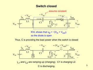
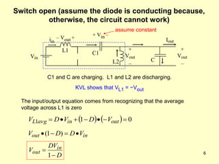
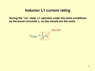
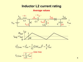
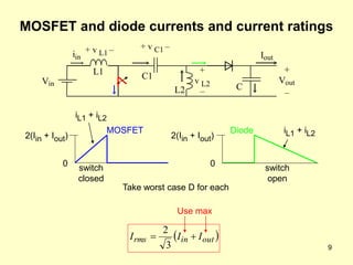
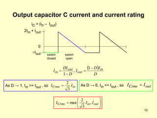
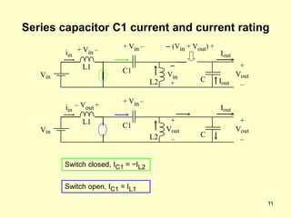
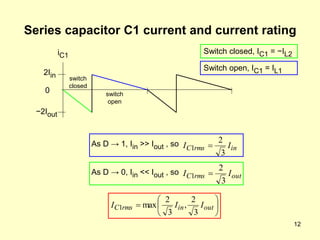
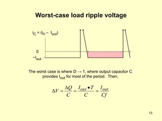
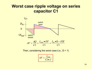
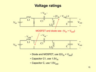
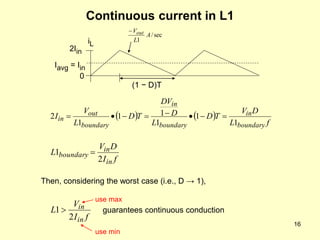
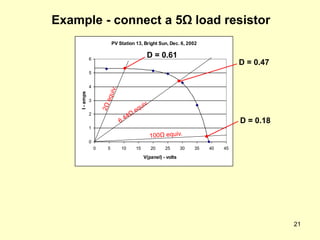
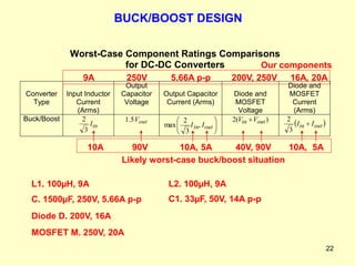
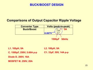
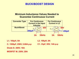
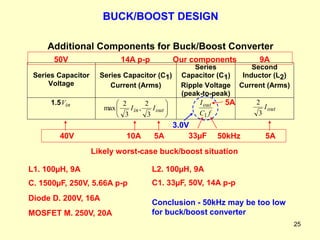
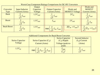
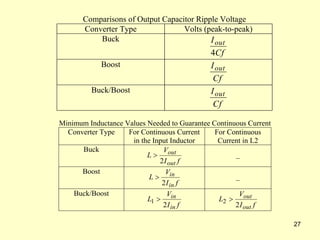
1
EE462L, Fall 2011
DC−DC Buck/Boost Converter
2
Boost converter
+
Vout
–
Iout
C
Vin
iin
L1
+ v L1 –
Buck/Boost converter
+
v L2
–
C1
+ v C1 –
L2
Vin
iin
L1
+ v L1 –
+
v L2
–
C1
+ v C1 –
L2
+
Vout
–
Iout
C
3
Buck/Boost converter
This circuit is more unforgiving than the boost converter, because the
MOSFET and diode voltages and currents are higher
• Before applying power, make sure that your D is at
the minimum, and that a load is solidly connected
• Limit your output voltage to 90V
Vin
iin
L1
+ v L1 –
+
v L2
–
C1
+ v C1 –
L2
+
Vout
–
Iout
C
4
+
Vout
–
Iout
C
Vin
Iin
L1
+ 0 –
+
0
–
KVL and KCL in the average sense
0
0
Iout
Iin
C1
L2
Iout
+ Vin –
KVL shows that VC1 = Vin
Interestingly, no average current passes from the source side, through
C1, to the load side, and yet this is a “DC - DC” converter
5
Switch closed
Vin
iin
L1
+ Vin –
+
v L2
–
C1
+ Vin –
L2
+
Vout
–
Iout
C
assume constant
+ v D –
KVL shows that vD = −(Vin + Vout),
so the diode is open
Thus, C is providing the load power when the switch is closed
Vin
iin
L1 –
Vin
+
C1
+ Vin –
L2
+
Vout
–
Iout
C
– (Vin + Vout) +
Iout
iL1 and iL2 are ramping up (charging). C1 is charging L2.
C is discharging.
+ Vin –
6
Switch open (assume the diode is conducting because,
otherwise, the circuit cannot work)
Vin
iin
L1
– Vout +
C1
+ Vin –
L2
+
Vout
–
Iout
C
C1 and C are charging. L1 and L2 are discharging.
+
Vout
–
KVL shows that VL1 = −Vout
    0
1
1 





 out
in
avg
L V
D
V
D
V
in
out V
D
D
V 


 )
1
(
D
DV
V in
out


1
The input/output equation comes from recognizing that the average
voltage across L1 is zero
assume constant
7
Inductor L1 current rating
in
rms
L I
I
3
2
1 
Use max
During the “on” state, L1 operates under the same conditions
as the boost converter L, so the results are the same
8
Inductor L2 current rating
  2
2
2
2
2
3
4
2
12
1
out
out
out
rms
L I
I
I
I 



out
rms
L I
I
3
2
2 
2Iout
0
Iavg = Iout
ΔI
iL2
Use max
+
Vout
–
Iout
C
Vin
Iin
L1
+ 0 –
+
0
–
0
0
Iout
Iin
C1
L2
Iout
+ Vin –
Average values
9
MOSFET and diode currents and current ratings
0
2(Iin + Iout)
0
Take worst case D for each
Vin
iin
L1
+ v L1 –
+
v L2
–
C1
+ v C1 –
L2
+
Vout
–
Iout
C
MOSFET Diode iL1 + iL2
 
out
in
rms I
I
I 

3
2
Use max
switch
closed
switch
open
2(Iin + Iout)
iL1 + iL2
10
Output capacitor C current and current rating
in
Crms I
I
3
2
 out
Crms I
I 
2Iin + Iout
−Iout
0
As D → 1, Iin >> Iout , so
iC = (iD – Iout)
As D → 0, Iin << Iout , so
 
D
I
D
I
D
DI
I in
out
out
in




1
,
1






 out
in
Crms I
I
I ,
3
2
max
switch
closed
switch
open
11
Series capacitor C1 current and current rating
Switch closed, IC1 = −IL2
Vin
iin
L1 –
Vin
+
C1
+ Vin –
L2
+
Vout
–
Iout
C
– (Vin + Vout) +
Iout
+ Vin –
Vin
iin
L1
– Vout +
C1
+ Vin –
L2
+
Vout
–
Iout
C
+
Vout
–
Switch open, IC1 = IL1
12
Series capacitor C1 current and current rating
in
rms
C I
I
3
2
1 
2Iin
−2Iout
0
As D → 1, Iin >> Iout , so
iC1
As D → 0, Iin << Iout , so






 out
in
rms
C I
I
I
3
2
,
3
2
max
1
switch
closed
switch
open
out
rms
C I
I
3
2
1 
Switch closed, IC1 = −IL2
Switch open, IC1 = IL1
13
Worst-case load ripple voltage
Cf
I
C
T
I
C
Q
V out
out 





The worst case is where D → 1, where output capacitor C
provides Iout for most of the period. Then,
−Iout
0
iC = (iD – Iout)
14
Worst case ripple voltage on series
capacitor C1
2Iin
−2Iout
0
iC1
f
C
I
V out



1
switch
closed
switch
open
 
1
1
1
1 C
T
D
I
C
DT
I
C
Q
V in
out 







Then, considering the worst case (i.e., D = 1)
15
Voltage ratings
MOSFET and diode see (Vin + Vout)
• Diode and MOSFET, use 2(Vin + Vout)
• Capacitor C1, use 1.5Vin
• Capacitor C, use 1.5Vout
Vin
L1 C1
+ Vin –
L2
+
Vout
–
C
– (Vin + Vout) +
Vin
L1
– Vout +
C1
+ Vin –
L2
+
Vout
–
C
16
Continuous current in L1
sec
/
1
A
L
Vout

   
f
L
D
V
T
D
L
D
DV
T
D
L
V
I
boundary
in
boundary
in
boundary
out
in
1
1
1
1
1
1
2 







f
I
D
V
L
in
in
boundary
2
1 
2Iin
0
Iavg = Iin
iL
(1 − D)T
f
I
V
L
in
in
2
1 guarantees continuous conduction
Then, considering the worst case (i.e., D → 1),
use max
use min
17
Continuous current in L2
sec
/
2
A
L
Vout

f
L
D
V
T
D
L
V
I
boundary
out
boundary
out
out
2
)
1
(
)
1
(
2
2





2Iout
0
Iavg = Iout
iL
(1 − D)T
f
I
D
V
L
out
out
boundary
2
)
1
(
2


f
I
V
L
out
out
2
2  guarantees continuous conduction
Then, considering the worst case (i.e., D → 0),
use max
use min
18
Impedance matching
out
out
load
I
V
R 
equiv
R
 
 
load
out
out
out
out
in
in
equiv R
D
D
I
V
D
D
D
DI
D
V
D
I
V
R
2
2
1
1
1
1





 







 





DC−DC Boost
Converter
+
Vin
−
+
−
Iin
+
Vin
−
Iin
Equivalent from
source perspective
Source D
DV
V in
out


1
 
D
D
I
I in
out


1
19
Impedance matching
 
 
load
out
out
out
out
in
in
equiv R
D
D
I
V
D
D
D
DI
D
V
D
I
V
R
2
2
1
1
1
1





 







 





For any Rload, as D → 0, then Requiv → ∞ (i.e., an open circuit)
For any Rload, as D → 1, then Requiv → 0 (i.e., a short circuit)
Thus, the buck/boost converter can sweep the entire I-V
curve of a solar panel
20
Example - connect a 100Ω load resistor
PV Station 13, Bright Sun, Dec. 6, 2002
0
1
2
3
4
5
6
0 5 10 15 20 25 30 35 40 45
V(panel) - volts
I
-
amps
D = 0.80
D = 0.50
D = 0.88
With a 100Ω load resistor attached, raising D from 0 to 1 moves the solar
panel load from the open circuit condition to the short circuit condition
21
Example - connect a 5Ω load resistor
PV Station 13, Bright Sun, Dec. 6, 2002
0
1
2
3
4
5
6
0 5 10 15 20 25 30 35 40 45
V(panel) - volts
I
-
amps
D = 0.47
D = 0.18
D = 0.61
22
Worst-Case Component Ratings Comparisons
for DC-DC Converters
Converter
Type
Input Inductor
Current
(Arms)
Output
Capacitor
Voltage
Output Capacitor
Current (Arms)
Diode and
MOSFET
Voltage
Diode and
MOSFET
Current
(Arms)
Buck/Boost
in
I
3
2 1.5 out
V






out
in I
I ,
3
2
max
)
(
2 out
in V
V 
 
out
in I
I 
3
2
5.66A p-p 200V, 250V 16A, 20A
Our components
9A 250V
10A, 5A
10A 90V 40V, 90V
Likely worst-case buck/boost situation
10A, 5A
MOSFET M. 250V, 20A
L1. 100µH, 9A
C. 1500µF, 250V, 5.66A p-p
Diode D. 200V, 16A
L2. 100µH, 9A
C1. 33µF, 50V, 14A p-p
BUCK/BOOST DESIGN
23
Comparisons of Output Capacitor Ripple Voltage
Converter Type Volts (peak-to-peak)
Buck/Boost
Cf
Iout 5A
1500µF 50kHz
0.067V
MOSFET M. 250V, 20A
L1. 100µH, 9A
C. 1500µF, 250V, 5.66A p-p
Diode D. 200V, 16A
L2. 100µH, 9A
C1. 33µF, 50V, 14A p-p
BUCK/BOOST DESIGN
24
Minimum Inductance Values Needed to
Guarantee Continuous Current
Converter Type For Continuous
Current in the Input
Inductor
For Continuous
Current in L2
Buck/Boost
f
I
V
L
in
in
2
1 
f
I
V
L
out
out
2
2 
40V
2A 50kHz
200µH
90V
2A 50kHz
450µH
MOSFET M. 250V, 20A
L1. 100µH, 9A
C. 1500µF, 250V, 5.66A p-p
Diode D. 200V, 16A
L2. 100µH, 9A
C1. 33µF, 50V, 14A p-p
BUCK/BOOST DESIGN
25
Additional Components for Buck/Boost Converter
Series Capacitor
Voltage
Series Capacitor (C1)
Current (Arms)
Series
Capacitor (C1)
Ripple Voltage
(peak-to-peak)
Second
Inductor (L2)
Current (Arms)
1.5 in
V








out
in I
I
3
2
,
3
2
max
f
C
Iout
1
out
I
3
2
MOSFET M. 250V, 20A
L1. 100µH, 9A
C. 1500µF, 250V, 5.66A p-p
Diode D. 200V, 16A
L2. 100µH, 9A
C1. 33µF, 50V, 14A p-p
10A 5A
40V
Likely worst-case buck/boost situation
5A
5A
33µF 50kHz
3.0V
BUCK/BOOST DESIGN
Our components 9A
14A p-p
50V
Conclusion - 50kHz may be too low
for buck/boost converter
26
Worst-Case Component Ratings Comparisons for DC-DC Converters
Converter
Type
Input Inductor
Current (Arms)
Output
Capacitor
Voltage
Output Capacitor
Current (Arms)
Diode and
MOSFET Voltage
Diode and
MOSFET
Current (Arms)
Buck
out
I
3
2 1.5 out
V
out
I
3
1 2 in
V
out
I
3
2
Boost
in
I
3
2 1.5 out
V out
I 2 out
V
in
I
3
2
Buck/Boost
in
I
3
2 1.5 out
V








out
in I
I ,
3
2
max
 
out
in V
V 
2
 
out
in I
I 
3
2
Additional Components for Buck/Boost Converter
Series Capacitor
Voltage
Series Capacitor (C1)
Current (Arms)
Series Capacitor
(C1) Ripple
Voltage (peak-to-
peak)
Second Inductor
(L2) Current
(Arms)
1.5 in
V








out
in I
I
3
2
,
3
2
max
f
C
Iout
1
out
I
3
2
27
Comparisons of Output Capacitor Ripple Voltage
Converter Type Volts (peak-to-peak)
Buck
Cf
Iout
4
Boost
Cf
Iout
Buck/Boost
Cf
Iout
Minimum Inductance Values Needed to Guarantee Continuous Current
Converter Type For Continuous Current
in the Input Inductor
For Continuous
Current in L2
Buck
f
I
V
L
out
out
2
 –
Boost
f
I
V
L
in
in
2
 –
Buck/Boost
f
I
V
L
in
in
2
1 
f
I
V
L
out
out
2
2 

_8_EE462L_Fall2011_DC_DC_BuckBoost_PPT.ppt

  • 1.
    1 EE462L, Fall 2011 DC−DCBuck/Boost Converter
  • 2.
    2 Boost converter + Vout – Iout C Vin iin L1 + vL1 – Buck/Boost converter + v L2 – C1 + v C1 – L2 Vin iin L1 + v L1 – + v L2 – C1 + v C1 – L2 + Vout – Iout C
  • 3.
    3 Buck/Boost converter This circuitis more unforgiving than the boost converter, because the MOSFET and diode voltages and currents are higher • Before applying power, make sure that your D is at the minimum, and that a load is solidly connected • Limit your output voltage to 90V Vin iin L1 + v L1 – + v L2 – C1 + v C1 – L2 + Vout – Iout C
  • 4.
    4 + Vout – Iout C Vin Iin L1 + 0 – + 0 – KVLand KCL in the average sense 0 0 Iout Iin C1 L2 Iout + Vin – KVL shows that VC1 = Vin Interestingly, no average current passes from the source side, through C1, to the load side, and yet this is a “DC - DC” converter
  • 5.
    5 Switch closed Vin iin L1 + Vin– + v L2 – C1 + Vin – L2 + Vout – Iout C assume constant + v D – KVL shows that vD = −(Vin + Vout), so the diode is open Thus, C is providing the load power when the switch is closed Vin iin L1 – Vin + C1 + Vin – L2 + Vout – Iout C – (Vin + Vout) + Iout iL1 and iL2 are ramping up (charging). C1 is charging L2. C is discharging. + Vin –
  • 6.
    6 Switch open (assumethe diode is conducting because, otherwise, the circuit cannot work) Vin iin L1 – Vout + C1 + Vin – L2 + Vout – Iout C C1 and C are charging. L1 and L2 are discharging. + Vout – KVL shows that VL1 = −Vout     0 1 1        out in avg L V D V D V in out V D D V     ) 1 ( D DV V in out   1 The input/output equation comes from recognizing that the average voltage across L1 is zero assume constant
  • 7.
    7 Inductor L1 currentrating in rms L I I 3 2 1  Use max During the “on” state, L1 operates under the same conditions as the boost converter L, so the results are the same
  • 8.
    8 Inductor L2 currentrating   2 2 2 2 2 3 4 2 12 1 out out out rms L I I I I     out rms L I I 3 2 2  2Iout 0 Iavg = Iout ΔI iL2 Use max + Vout – Iout C Vin Iin L1 + 0 – + 0 – 0 0 Iout Iin C1 L2 Iout + Vin – Average values
  • 9.
    9 MOSFET and diodecurrents and current ratings 0 2(Iin + Iout) 0 Take worst case D for each Vin iin L1 + v L1 – + v L2 – C1 + v C1 – L2 + Vout – Iout C MOSFET Diode iL1 + iL2   out in rms I I I   3 2 Use max switch closed switch open 2(Iin + Iout) iL1 + iL2
  • 10.
    10 Output capacitor Ccurrent and current rating in Crms I I 3 2  out Crms I I  2Iin + Iout −Iout 0 As D → 1, Iin >> Iout , so iC = (iD – Iout) As D → 0, Iin << Iout , so   D I D I D DI I in out out in     1 , 1        out in Crms I I I , 3 2 max switch closed switch open
  • 11.
    11 Series capacitor C1current and current rating Switch closed, IC1 = −IL2 Vin iin L1 – Vin + C1 + Vin – L2 + Vout – Iout C – (Vin + Vout) + Iout + Vin – Vin iin L1 – Vout + C1 + Vin – L2 + Vout – Iout C + Vout – Switch open, IC1 = IL1
  • 12.
    12 Series capacitor C1current and current rating in rms C I I 3 2 1  2Iin −2Iout 0 As D → 1, Iin >> Iout , so iC1 As D → 0, Iin << Iout , so        out in rms C I I I 3 2 , 3 2 max 1 switch closed switch open out rms C I I 3 2 1  Switch closed, IC1 = −IL2 Switch open, IC1 = IL1
  • 13.
    13 Worst-case load ripplevoltage Cf I C T I C Q V out out       The worst case is where D → 1, where output capacitor C provides Iout for most of the period. Then, −Iout 0 iC = (iD – Iout)
  • 14.
    14 Worst case ripplevoltage on series capacitor C1 2Iin −2Iout 0 iC1 f C I V out    1 switch closed switch open   1 1 1 1 C T D I C DT I C Q V in out         Then, considering the worst case (i.e., D = 1)
  • 15.
    15 Voltage ratings MOSFET anddiode see (Vin + Vout) • Diode and MOSFET, use 2(Vin + Vout) • Capacitor C1, use 1.5Vin • Capacitor C, use 1.5Vout Vin L1 C1 + Vin – L2 + Vout – C – (Vin + Vout) + Vin L1 – Vout + C1 + Vin – L2 + Vout – C
  • 16.
    16 Continuous current inL1 sec / 1 A L Vout      f L D V T D L D DV T D L V I boundary in boundary in boundary out in 1 1 1 1 1 1 2         f I D V L in in boundary 2 1  2Iin 0 Iavg = Iin iL (1 − D)T f I V L in in 2 1 guarantees continuous conduction Then, considering the worst case (i.e., D → 1), use max use min
  • 17.
    17 Continuous current inL2 sec / 2 A L Vout  f L D V T D L V I boundary out boundary out out 2 ) 1 ( ) 1 ( 2 2      2Iout 0 Iavg = Iout iL (1 − D)T f I D V L out out boundary 2 ) 1 ( 2   f I V L out out 2 2  guarantees continuous conduction Then, considering the worst case (i.e., D → 0), use max use min
  • 18.
    18 Impedance matching out out load I V R  equiv R    load out out out out in in equiv R D D I V D D D DI D V D I V R 2 2 1 1 1 1                      DC−DC Boost Converter + Vin − + − Iin + Vin − Iin Equivalent from source perspective Source D DV V in out   1   D D I I in out   1
  • 19.
    19 Impedance matching    load out out out out in in equiv R D D I V D D D DI D V D I V R 2 2 1 1 1 1                      For any Rload, as D → 0, then Requiv → ∞ (i.e., an open circuit) For any Rload, as D → 1, then Requiv → 0 (i.e., a short circuit) Thus, the buck/boost converter can sweep the entire I-V curve of a solar panel
  • 20.
    20 Example - connecta 100Ω load resistor PV Station 13, Bright Sun, Dec. 6, 2002 0 1 2 3 4 5 6 0 5 10 15 20 25 30 35 40 45 V(panel) - volts I - amps D = 0.80 D = 0.50 D = 0.88 With a 100Ω load resistor attached, raising D from 0 to 1 moves the solar panel load from the open circuit condition to the short circuit condition
  • 21.
    21 Example - connecta 5Ω load resistor PV Station 13, Bright Sun, Dec. 6, 2002 0 1 2 3 4 5 6 0 5 10 15 20 25 30 35 40 45 V(panel) - volts I - amps D = 0.47 D = 0.18 D = 0.61
  • 22.
    22 Worst-Case Component RatingsComparisons for DC-DC Converters Converter Type Input Inductor Current (Arms) Output Capacitor Voltage Output Capacitor Current (Arms) Diode and MOSFET Voltage Diode and MOSFET Current (Arms) Buck/Boost in I 3 2 1.5 out V       out in I I , 3 2 max ) ( 2 out in V V    out in I I  3 2 5.66A p-p 200V, 250V 16A, 20A Our components 9A 250V 10A, 5A 10A 90V 40V, 90V Likely worst-case buck/boost situation 10A, 5A MOSFET M. 250V, 20A L1. 100µH, 9A C. 1500µF, 250V, 5.66A p-p Diode D. 200V, 16A L2. 100µH, 9A C1. 33µF, 50V, 14A p-p BUCK/BOOST DESIGN
  • 23.
    23 Comparisons of OutputCapacitor Ripple Voltage Converter Type Volts (peak-to-peak) Buck/Boost Cf Iout 5A 1500µF 50kHz 0.067V MOSFET M. 250V, 20A L1. 100µH, 9A C. 1500µF, 250V, 5.66A p-p Diode D. 200V, 16A L2. 100µH, 9A C1. 33µF, 50V, 14A p-p BUCK/BOOST DESIGN
  • 24.
    24 Minimum Inductance ValuesNeeded to Guarantee Continuous Current Converter Type For Continuous Current in the Input Inductor For Continuous Current in L2 Buck/Boost f I V L in in 2 1  f I V L out out 2 2  40V 2A 50kHz 200µH 90V 2A 50kHz 450µH MOSFET M. 250V, 20A L1. 100µH, 9A C. 1500µF, 250V, 5.66A p-p Diode D. 200V, 16A L2. 100µH, 9A C1. 33µF, 50V, 14A p-p BUCK/BOOST DESIGN
  • 25.
    25 Additional Components forBuck/Boost Converter Series Capacitor Voltage Series Capacitor (C1) Current (Arms) Series Capacitor (C1) Ripple Voltage (peak-to-peak) Second Inductor (L2) Current (Arms) 1.5 in V         out in I I 3 2 , 3 2 max f C Iout 1 out I 3 2 MOSFET M. 250V, 20A L1. 100µH, 9A C. 1500µF, 250V, 5.66A p-p Diode D. 200V, 16A L2. 100µH, 9A C1. 33µF, 50V, 14A p-p 10A 5A 40V Likely worst-case buck/boost situation 5A 5A 33µF 50kHz 3.0V BUCK/BOOST DESIGN Our components 9A 14A p-p 50V Conclusion - 50kHz may be too low for buck/boost converter
  • 26.
    26 Worst-Case Component RatingsComparisons for DC-DC Converters Converter Type Input Inductor Current (Arms) Output Capacitor Voltage Output Capacitor Current (Arms) Diode and MOSFET Voltage Diode and MOSFET Current (Arms) Buck out I 3 2 1.5 out V out I 3 1 2 in V out I 3 2 Boost in I 3 2 1.5 out V out I 2 out V in I 3 2 Buck/Boost in I 3 2 1.5 out V         out in I I , 3 2 max   out in V V  2   out in I I  3 2 Additional Components for Buck/Boost Converter Series Capacitor Voltage Series Capacitor (C1) Current (Arms) Series Capacitor (C1) Ripple Voltage (peak-to- peak) Second Inductor (L2) Current (Arms) 1.5 in V         out in I I 3 2 , 3 2 max f C Iout 1 out I 3 2
  • 27.
    27 Comparisons of OutputCapacitor Ripple Voltage Converter Type Volts (peak-to-peak) Buck Cf Iout 4 Boost Cf Iout Buck/Boost Cf Iout Minimum Inductance Values Needed to Guarantee Continuous Current Converter Type For Continuous Current in the Input Inductor For Continuous Current in L2 Buck f I V L out out 2  – Boost f I V L in in 2  – Buck/Boost f I V L in in 2 1  f I V L out out 2 2 