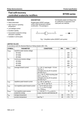
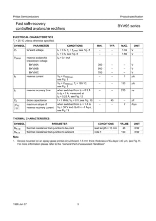
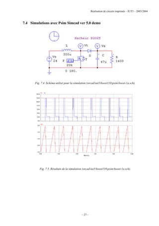
This document provides information about a boost converter circuit project including a list of documents, designation of components, images of key components, and simulation results. It lists 17 components used in the boost converter circuit including capacitors, diodes, an inductor, voltage regulator, resistors, transistor, and integrated circuit. It also includes figures of the circuit schematic used for simulation and results of the simulation.
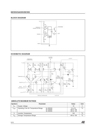
![Réalisation de circuits imprimés – IUT3 – 2003/2004
– 25 –
Projet 7 - BOOST110 / Hacheur élévateur de type
BOOST 24V / 110V-80mA
Projet : IUT3
Info : [DIV424]
Révision : 1 du samedi 14 février 2004
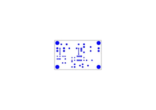
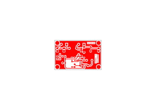
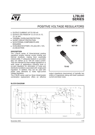
Fig. 7.1. Maquette (images-maquettesboost110-12.jpg).
7.1 Liste des documents
- Prix du montage.
- Schéma électronique.
- Circuit imprimé coté cuivre.
- Circuit imprimé coté composants.
- Implantation des composants.
- Documentations.](https://image.slidesharecdn.com/boost110-220605204821-baf74956/85/BOOST110-pdf-1-320.jpg)
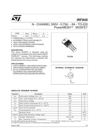
![Réalisation de circuits imprimés – IUT3 – 2003/2004
– 25 –
Projet 7 - BOOST110 / Hacheur élévateur de type
BOOST 24V / 110V-80mA
Projet : IUT3
Info : [DIV424]
Révision : 1 du samedi 14 février 2004
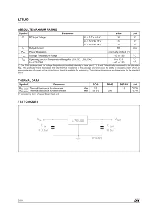
Fig. 7.1. Maquette (images-maquettesboost110-12.jpg).
7.1 Liste des documents
- Prix du montage.
- Schéma électronique.
- Circuit imprimé coté cuivre.
- Circuit imprimé coté composants.
- Implantation des composants.
- Documentations.](https://image.slidesharecdn.com/boost110-220605204821-baf74956/75/BOOST110-pdf-1-2048.jpg)
![Thierry LEQUEU – Juillet 2004 – [DATA076] – Fichier : PROJETS-IUT3.DOC
– 26 –
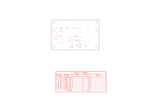
7.2 Désignation des composants
Tableau 7.1. Liste de composants (projets-iut3.xls / BOOST110).
No Quantité Référence Désignation Empreinte
1 1 C1 100uF 63V RADIAL06
2 1 C2 47uF 400V RADIAL13
3 1 C3 CAPA POL RADIAL06
4 4 C5,C6,C7,C9 100nF CK06
5 1 D1 BYV95C DO41
6 1 D2 1N4001 DO41
7 1 D3 BZT03C150 DO41
8 1 D4 3mm 2mA LED3
9 1 JP1 +110V 02PL2
10 1 JP2 24V 02PL2
11 1 L1 300uH 2A WE300
12 1 REG1 78L15 TO92
13 1 R2 6.8k RC04L
14 2 R3,R6 10k RC04L
15 2 R8,R9 10k AJ RAJ1
16 1 T1 IRF840 TO220
17 1 U2 NE555 08DIP300L
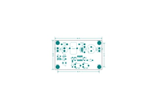
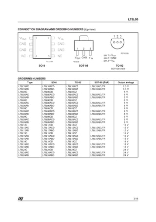
7.3 Allure des principaux composants
Fig. 7.2. Bornier CANDEM 3 points (images-composantsbornier1.jpg).
Fig. 7.3. Inductance série WE-FI Würth Elektronik (images-composantsWE300FI.jpg).](https://image.slidesharecdn.com/boost110-220605204821-baf74956/85/BOOST110-pdf-2-320.jpg)
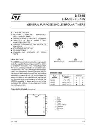
![Projet IUT3 / [DIV424] / BOOST110 1
Hacheur élévateur de type BOOST 24V / 110V-80mA
A4
1 1
Saturday, February 14, 2004
Title
Size Document Number Rev
Date: Sheet of
GATE
GATE
+24V +110V
+24V +15V +15V
D2
BYV95C
DO41
D1
1N4001
DO41
JP1
+110V
02PL2
1
2
JP2
24V
02PL2
1
2
+ C1
100uF 63V
RADIAL10
1
2
+ C2
47uF 400V
RADIAL18
1
2
+ C4
CAPA POL
RADIAL08
1
2
C7
100nF
CK06
C3
100nF
CK06
C6
1nF
CK06
D3
BZT03C150
DO41
REG1
78L15
TO92
3 1
2
Vi Vo
GND
D4
3mm 2mA
LED3
L1
300uH 2A
WE300
VIS3
VISSERIE
M3
1
1
VIS2
VISSERIE
M3
1
1
VIS1
VISSERIE
M3
1
1
VIS4
VISSERIE
M3
1
1
R1
10k
RC04L
R2
6.8k
RC04L
R4
10k AJ
RAJ1
1
3
2
R3
10k AJ
RAJ1
1
3
2
R5
10k
RC04L
T1
IRF840
TO220
1
2
3
C5
100nF
CK06
U1
NE555
08DIP300L
2
5
3
7
6
4
8
1
TR
CV
Q
DIS
THR
R
VCC
GND](https://image.slidesharecdn.com/boost110-220605204821-baf74956/85/BOOST110-pdf-4-320.jpg)