Recommended
PDF
microelectronics-6ed-ch7_a-ppt-2025-spring
PDF
PDF
Comparison of CMOS Current Mirror Sources
PPTX
Basic electrical properties for VLSI syllabus topic
PDF
"Comprehensive Guide to PMOS Transistors"
PDF
V3_Multistage Amplifier n Current Mirror.pdf
PPTX
PDF
High Speed, Broadband Amplifiers.pdf
PPT
aet 402 lecture1.ppt vlsi CIRCUIT DESIGN
PDF
PPT
PPTX
Elecrical Propertiesddfafafafafafafav.pptx
DOCX
vlsi qb.docx imprtant questions for all units
PDF
Transisotor-MOSFETS Basics Operation.pdf
PDF
PPT
basic_CMOS_technology_CERN_GENEVA_SWITZERLAND.ppt
PPT
FALLSEM2023-24_BECE303L_TH_VL2023240100242_2023-04-24_Reference-Material-I.ppt
PPT
MOSFET.ppt NPN -PNP -Operations-Early effect-Current equations – Input and Ou...
PPT
MOSFET.ppt NPN -PNP -Operations-Early effect-Current equations – Input and Ou...
PPT
MOSFET.ppt NPN -PNP -Operations-Early effect-Current equations – Input and Ou...
PPT
MOSFET WORKING PRINCIPLE and GRAPH EXPLANATIONS
PPT
MOSFET structure charateisics biasing.ppt
PPT
MOSFET operation characteristics and types
PPT
PPT
MOSFET analysis VI characteristics and dc analysis
PDF
PDF
LSI_Logic_Design_Chapter_2_for_computer_engineer.pdf
PPT
CMOS transistor and its concepts related
PDF
The 8 Best Marketplaces for Selling and Buying Social Media Accounts.pdf
PPTX
control and connectivity.pptx microcontroller
More Related Content
PDF
microelectronics-6ed-ch7_a-ppt-2025-spring
PDF
PDF
Comparison of CMOS Current Mirror Sources
PPTX
Basic electrical properties for VLSI syllabus topic
PDF
"Comprehensive Guide to PMOS Transistors"
PDF
V3_Multistage Amplifier n Current Mirror.pdf
PPTX
PDF
High Speed, Broadband Amplifiers.pdf
Similar to Layout of current mirror by taking some example
PPT
aet 402 lecture1.ppt vlsi CIRCUIT DESIGN
PDF
PPT
PPTX
Elecrical Propertiesddfafafafafafafav.pptx
DOCX
vlsi qb.docx imprtant questions for all units
PDF
Transisotor-MOSFETS Basics Operation.pdf
PDF
PPT
basic_CMOS_technology_CERN_GENEVA_SWITZERLAND.ppt
PPT
FALLSEM2023-24_BECE303L_TH_VL2023240100242_2023-04-24_Reference-Material-I.ppt
PPT
MOSFET.ppt NPN -PNP -Operations-Early effect-Current equations – Input and Ou...
PPT
MOSFET.ppt NPN -PNP -Operations-Early effect-Current equations – Input and Ou...
PPT
MOSFET.ppt NPN -PNP -Operations-Early effect-Current equations – Input and Ou...
PPT
MOSFET WORKING PRINCIPLE and GRAPH EXPLANATIONS
PPT
MOSFET structure charateisics biasing.ppt
PPT
MOSFET operation characteristics and types
PPT
PPT
MOSFET analysis VI characteristics and dc analysis
PDF
PDF
LSI_Logic_Design_Chapter_2_for_computer_engineer.pdf
PPT
CMOS transistor and its concepts related
Recently uploaded
PDF
The 8 Best Marketplaces for Selling and Buying Social Media Accounts.pdf
PPTX
control and connectivity.pptx microcontroller
PPTX
Sensors and Actuators in IoT Systems.pptx
PPTX
2. Compressor ppt Ashish 2 made to learn.pptx
PDF
Introduction to IBM Power - 2024-Nov-09.PDF
PDF
E catalogue solar panel cleaner Leopard Dust-Your better solar panel cleaning...
PDF
Best 5 Way to Buy Google Ads Accounts - Modern - New York.pdf
PPTX
Osteoporosis management medical managment
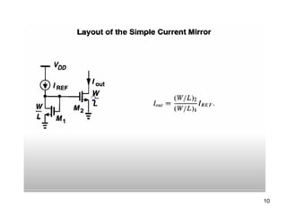
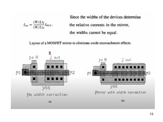
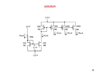
Layout of current mirror by taking some example 1. 2. Tutorial Questions
• Consider the triple cascode current
sink .assume all transistors operating in
saturation region with Id=10μA, Vds=50 V,
amplification factor gmr0=50. find the
value of output resistance. Neglect the
bulk effect.
• draw the circuit diagram of PMOS
cascode current mirror.
www.satishkashyap.com 2
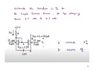
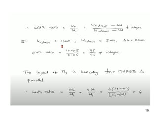
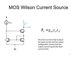
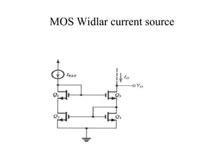
3. 4. 5. 6. 7. 8. 9. 10. 11. 12. 13. 14. 15. 16. 17. 18. 19. MOS Wilson Current Source
19
2
3
3 o
o
m
o r
r
g
R
The drain current of Q2 to equal
the input current and the output
configuration assures that the
output current equals the drain
current of Q1.
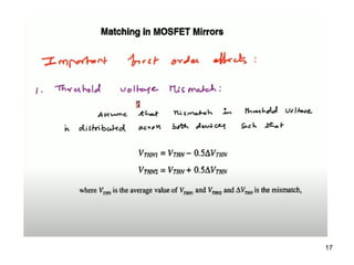
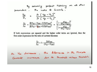
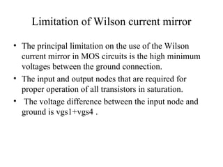
20. Limitation of Wilson current mirror
• The principal limitation on the use of the Wilson
current mirror in MOS circuits is the high minimum
voltages between the ground connection.
• The input and output nodes that are required for
proper operation of all transistors in saturation.
• The voltage difference between the input node and
ground is vgs1+vgs4 .
21. 22. 23. 23
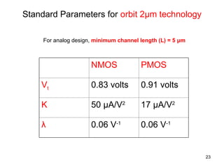
Standard Parameters for orbit 2μm technology
NMOS PMOS
Vt 0.83 volts 0.91 volts
K 50 μA/V2
17 μA/V2
λ 0.06 V-1
0.06 V-1
For analog design, minimum channel length (L) = 5 μm
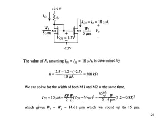
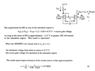
24. 25. 26. 27. 28. 29. 30. 31. 31
For PMOS, drain current in saturation region is
ID = (KP/2)W/L (VSG - Vtp)2
Substitute known values and calculate the value of Width of
PMOS transistor.
W = 70 μm
32.