KICKBACK NOISE ANALYSIS OF LOW POWER COMPARATOR
•
1 like•618 views

The need for ultra low-power, area efficient, and high speed analog-to-digital converters is pushing toward the use of dynamic regenerative comparators to maximize speed and power efficiency. In this report, an analysis on the delay of the dynamic comparators will be presented. Based on the presented analysis, a new dynamic comparator is proposed, where the circuit of a conventional doubletail comparator is modified for low-power and fast operation even in small supply voltages. Comparators presented in this paper designed with 180nm technology file. The power consumption and delay has been modified with tradeoff in area.

Recommended
Recommended
More Related Content
What's hot
What's hot (19)
Similar to KICKBACK NOISE ANALYSIS OF LOW POWER COMPARATOR
Similar to KICKBACK NOISE ANALYSIS OF LOW POWER COMPARATOR (20)
More from ijsrd.com
More from ijsrd.com (20)
Recently uploaded
Recently uploaded (20)
KICKBACK NOISE ANALYSIS OF LOW POWER COMPARATOR
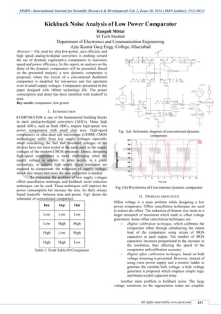
- 1. IJSRD - International Journal for Scientific Research & Development| Vol. 2, Issue 10, 2014 | ISSN (online): 2321-0613 All rights reserved by www.ijsrd.com 452 Kickback Noise Analysis of Low Power Comparator Rangoli Mittal M.Tech Student Department of Electronics and Communication Engineering Ajay Kumar Garg Engg. College, Ghaziabad Abstract— The need for ultra low-power, area efficient, and high speed analog-to-digital converters is pushing toward the use of dynamic regenerative comparators to maximize speed and power efficiency. In this report, an analysis on the delay of the dynamic comparators will be presented. Based on the presented analysis, a new dynamic comparator is proposed, where the circuit of a conventional doubletail comparator is modified for low-power and fast operation even in small supply voltages. Comparators presented in this paper designed with 180nm technology file. The power consumption and delay has been modified with tradeoff in area. Key words: comparator, low power I. INTRODUCTION COMPARATOR is one of the fundamental building blocks in most analog-to-digital converters (ADCs). Many high speed ADCs, such as flash ADCs, require high-speed, low power comparators with small chip area. High-speed comparators in ultra deep sub micrometer (UDSM) CMOS technologies suffer from low supply voltages especially when considering the fact that threshold voltages of the devices have not been scaled at the same pace as the supply voltages of the modern CMOS processes .Hence, designing high-speed comparators is more challenging when the supply voltage is smaller. In other words, in a given technology, to achieve high speed, larger transistors are required to compensate the reduction of supply voltage, which also means that more die area and power is needed. To overcome the problem of low supply voltages offset cancellation technique and kickback noise reduction techniques can be used. These techniques will improve the power consumption but increase the area. So there always found tradeoffs between area and power. Fig1 shows the schematic of conventional comparator. Inn Inp Out Low Low Low Low High High High Low High High High Low Table 1: Truth Table Of Comparator Fig. 1(a): Schematic diagram of conventional dynamic comparator. Fig.1(b):Waveforms of Conventional dynamic comparator II. PROBLEM ASSOCIATED Offset voltage is a main problem while designing a low power comparator. Offset cancellation techniques are used to reduce the effect. The reduction of feature size leads to a larger mismatch of transistors which leads to offset voltage generation. Some offset cancellation techniques are: Digital calibration technique, which calibrates the comparator offset through unbalancing the output load of the comparator using arrays of MOS capacitors at each output. The number of MOS capacitors increases proportional to the increase in the resolution, thus affecting the speed of the comparator and calibration accuracy. Digital offset calibration technique, based on bulk voltage trimming is presented. However, instead of using extra power supply and a resistor ladder to generate the variable bulk voltage, a bulk voltage generator is proposed which employs simple logic and binary-scaled capacitor array. Another main problem is kickback noise. The large voltage variations on the regeneration nodes are coupled,
- 2. Kickback Noise Analysis of Low Power Comparator (IJSRD/Vol. 2/Issue 10/2014/104) All rights reserved by www.ijsrd.com 453 through the parasitic capacitances of the transistors, to the input of the comparator. Since the circuit preceding it does not have zero output impedance, the input voltage is disturbed, which may degrade the accuracy of the converter. These disturbances usually called kickback noise. Techniques for Kickback noise reduction are: Neutralization Technique Insertion of MOS switches III. WORKING OF DYNAMIC COMPARATOR A. Conventional Comparator: The schematic diagram of the conventional dynamic comparator widely used in A/D converters, with high input impedance, rail-to-rail output swing, and no static power consumption is shown in Fig. 1 B. Double tail dynamic comparator: A conventional double-tail comparator is shown in Fig. 2 . This topology has less stacking and therefore can operate at lower supply voltages compared to the conventional dynamic comparator. The double tail enables both a large current in the latching stage and wider Mtail2, for fast latching independent of the input common-mode voltage (Vcm), and a small current in the input stage (small Mtail1), for low offset. Fig. 2(a): Double Tail Dynamic Comparator Fig. 2(b): Waveforms obtained for Double Tail Dynamic Comparator IV. SIMULATION RESULTS DELAY POWER Itail BASIC COMPARATOR 10µs 63µW 0.88µA DOUBLE TAIL COMPARATOR 20µs 16.1µW 3.6µA A. Kickback Noise: Principally in latched comparators, the large voltage variations on the regeneration nodes are coupled, through the parasitic capacitances of the transistors, to the input of the comparator. Since the circuit preceding it does not have zero output impedance, the input voltage is disturbed, which may degrade the accuracy of the converter. This disturbance is usually called ―kickback noise‖ it has been proved that the fastest and most power efficient comparators generate more kickback noise. Fig.3(a) shows the waveforms of Kickback Noise for Double Tail Comparator. Fig.3(b) shows the waveforms of Kickback Noise for Cascaded Double Tail Comparator. Kickback noise is a very crucialterm in ase of dynamic comparators. It is notthing but the varations come in the input node after latching. When complexity of circuit incresed then kickback noise also increased. There are some techniques to reduce this but this can not be removed permanntly from he circuitary. Table 3.3 shows the Comparison Of Kickback Noises of different comparators. Table 3.4 shows the analysis of Cascaded Double Tail Comparator based on different parameters. B. Comparison Of Kickback Noise: COMPARATOR’S STYLE KICKBACK NOISE Conventional comparator 70mV Double Tail Comparator 43mV Cascaded Double Tail Comparator 50mV Fig. 3(a): Kickback Noise for Double Tail Comparator
- 3. Kickback Noise Analysis of Low Power Comparator (IJSRD/Vol. 2/Issue 10/2014/104) All rights reserved by www.ijsrd.com 454 Fig. 3(b): Kickback Noise for Cascaded Double Tail Comparator V. CONCLUSION It is concluded that the change in different cascading methods result in performance improvement or degradation. Different methods work on different parameters to give the tradeoff between theoretical performance evaluation and simulation or practical implementation.. Delay is always inversly proportional to the tail current, depends on switching capabi;ity of the device. REFERENCES [1] M. Maymandi-Nejad and M. Sachdev, ―1-bit quantiser with rail to rail input range for sub-1V ∑ modulators,‖ IEEE Electron. Lett., vol. 39,no. 12, pp. 894–895, Jan. 2003.. [2] A. Nikoozadeh and B. Murmann, ―An analysis of latched comaprator offset due to load capacitor mismatch,‖ IEEE Trans. Circuits Syst. II, Exp. Briefs, vol. 53, no. 12, pp. 1398–1402, Dec. 2006.. [3] P. M. Figueiredo and J. C. Vital, ―Kickback noise reduction techniques for CMOS latched comapartors,‖ IEEE Trans. Circuits Syst. II, Exp. Briefs, vol. 53, no. 7, pp. 541–545, Jul. 2006. [4] Samaneh Babayan Mashhadi and Reza Lotfi ― Analysis and Design of a Low Voltage Low Power Double Tail Comparator‖ IEEE Trans.,Jan.2013.