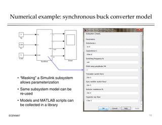
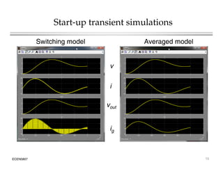
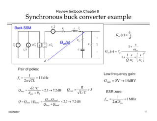
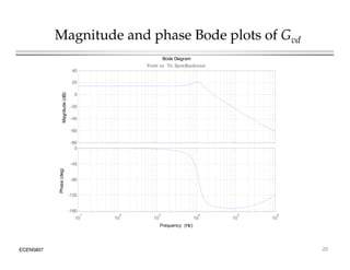
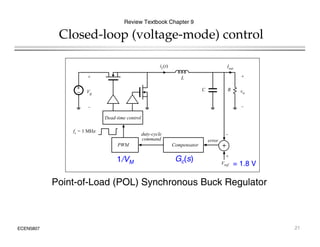
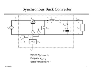
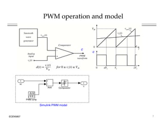
This document introduces switched-mode converter modeling using MATLAB/Simulink, focusing on building sophisticated control models and simulating systems within this environment. It highlights the unique capabilities of Simulink for system modeling while noting its limitations as a circuit simulator and the need for add-ons for traditional circuit simulations. Various aspects of modeling synchronous buck converters, including linearization and frequency response, are explored through examples and simulations.


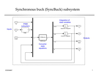
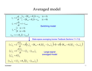
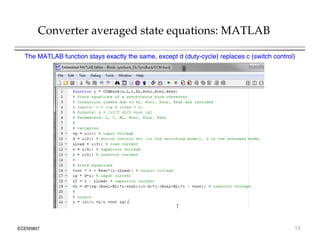
![Converter state equations: embedded MATLAB script
1
3
vout
2
i
1
v
1
s
inductor integrator
1
s
capacitor integrator
v c c
PWM
u y
CCMbuck
CCM buck
3
iLoad
2
vc
1
vg
dv /dt v
i
di/dt
v out
y
u
c
c
u = inputs = [vg c iLoad v i]
y = outputs = [ic/C vL/L vout ig]
u y
4
ig
ig
Converter
state
equations
i
i
R
v
v
)
0
(
)
1
(
0
c
c
i
ig
Load
esr
out i
i
R
v
v
)
1
(
1
c
v
i
R
R
v
di
L out
L
on
g
Load
C i
i
dt
dv
C
i
ECEN5807 8
)
0
(
)
(
2
1
c
v
i
R
R
dt
L
v
out
L
on
out
L
on
g
L](https://image.slidesharecdn.com/introductiontoswitched-modeconvertermodelingusingmatlab-simulink-241226042207-0c9ad144/85/Introduction-to-Switched-Mode-Converter-Modeling-using-MATLAB-Simulink-pdf-8-320.jpg)