This document provides an introduction to designing and simulating a simple logic circuit using Altera's Quartus II software. It describes how to:
1. Create a new project in Quartus II and specify the target FPGA device.
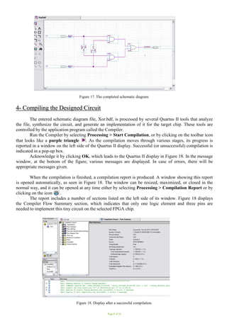
2. Design the circuit using a schematic diagram by importing logic gates and input/output pins from symbol libraries and connecting them with wires.
3. Simulate the designed circuit to verify its functionality before programming the FPGA.


![New_Microsoft_PowerPoint_Presentation-1[1].pdf](https://cdn.slidesharecdn.com/ss_thumbnails/newmicrosoftpowerpointpresentation-11-250106232808-51c69f09-thumbnail.jpg?width=640&height=640&fit=bounds)