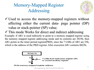
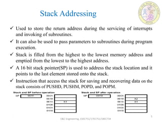
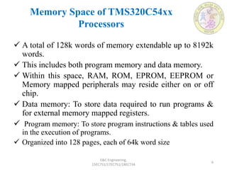
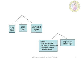
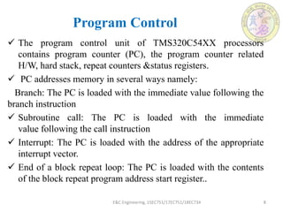
Department of Collegiate and Technical Education
DSPALGORITHM AND ARCHITECTURE
(15EC751/17EC751/18EC734)
Module 3
PROGRAMMABLE DIGITAL SIGNAL
PROCESSORS
SESSION 5
E&C Engineering, 15EC751/17EC751/18EC734
1
 To understand the data addressing modes of
TMS320C54xx processors.
 To understand Memory space and Program Control of
TMS320C54XX processors.
Learning objectives
E&C Engineering, 15EC751/17EC751/18EC734 2
 Memory Mapped Register AM
Stack AM
 Memory space of TMS320C54XX
Program Control of TMS320C54XX
Table of Content
E&C Engineering, 15EC751/17EC751/18EC734
3
Memory-Mapped Register
Addressing
E&C Engineering, 15EC751/17EC751/18EC734
4
 Used to access the memory-mapped registers without
affecting either the current data- page pointer (DP)
value or stack-pointer (SP) value.
 This mode Works for direct and indirect addressing
Example: if AR1 is used indirectly to point to a memory mapped register using
the memory mapped register addressing mode and its contents are 3825h, then
AR1 points to the timer period register(PRD), since the 7 LSBs of AR1 are 25h,
which is the address of the PRD register. After execution AR1 contains 0025h.
Stack Addressing
 Used to store the return address during the servicing of interrupts
and invoking of subroutines.
 It can also be used to pass parameters to subroutines during program
execution.
 Stack is filled from the highest to the lowest memory address and
emptied from the lowest to the highest address.
 A 16 bit stack pointer(SP) is used to address the stack location and it
points to the last element stored onto the stack.
 Instruction that access the stack for saving and recovering data on the
stack consists of PUSHD, PUSHM, POPD, and POPM.
E&C Engineering, 15EC751/17EC751/18EC734
5
Memory Space of TMS320C54xx
Processors
E&C Engineering,
15EC751/17EC751/18EC734
6
 A total of 128k words of memory extendable up to 8192k
words.
 This includes both program memory and data memory.
 Within this space, RAM, ROM, EPROM, EEPROM or
Memory mapped peripherals may reside either on or off
chip.
 Data memory: To store data required to run programs &
for external memory mapped registers.
 Program memory: To store program instructions & tables used
in the execution of programs.
 Organized into 128 pages, each of 64k word size
E&C Engineering, 15EC751/17EC751/18EC734 7
Program Control
 The program control unit of TMS320C54XX processors
contains program counter (PC), the program counter related
H/W, hard stack, repeat counters &status registers.
 PC addresses memory in several ways namely:
Branch: The PC is loaded with the immediate value following the
branch instruction
 Subroutine call: The PC is loaded with the immediate
value following the call instruction
 Interrupt: The PC is loaded with the address of the appropriate
interrupt vector.
 End of a block repeat loop: The PC is loaded with the contents
of the block repeat program address start register..
E&C Engineering, 15EC751/17EC751/18EC734 8
E&C Engineering, 15EC751/17EC751/18EC734 9
 End of a block repeat loop: The PC is loaded with the
contents of the block repeat program address start register.
Return: The PC is loaded from the top of the stack.
 The program counter-related hardware PAGEN provides
for the above options.
 The stack is used to save and restore the PC value during
subroutine calls and interrupts. It can also be used to save
and restore the accumulator low word or a data memory
value when required.
 ‘54xx processors provide hardware support for repetitive
execution of either a single instruction or a block of
instructions. Repeat counters are used for this purpose.
E&C Engineering, 15EC751/17EC751/18EC734 10
 A single instructions can be repeated N+1 times by
loading the value N in the repeat counter
register(RC).
 A block of instructions can be repeated N+1 times by
loading the value N in the repeat counter
register(RC).
LEARNING OUTCOME
To understand and remember Memory mapped
and Stack addressing modes of
TMS320C54XX device.
 Also to understand and remember Memory
space and program control of TMS320C54XX.
E&C Engineering, 15EC751/17EC751/18EC734
11
REFERENCES:
“Digital Signal Processing”, Avatar Singh and S.
Srinivasan, Thomson Learning, 2004.
REFERENCE BOOKS:
1.Digital Signal Processing: A practical approach, Ifeachor
E. C., Jervis B. W Pearson- Education, PHI/ 2002
2.“Digital Signal Processors”, B Venkataramani and M
Bhaskar TMH, 2002
3. “Architectures for Digital Signal Processing”, Peter
Pirsch John Weily, 2007
E&C Engineering, 15EC751/17EC751/18EC734
12
CHAIRMAN : Dr. Rangaraju
H.O.D : Dr Revanna C R
Content Developer: Prof.Hemanth kumar C S
Moderator: Prof.Hemanth Kumar C S
Prof. Roopashree D
E&C Engineering, 15EC751/17EC751/18EC734
13
QUESTIONS ?
E&C Engineering, 15EC751/17EC751/18EC734
14

ECE_18EC734_M3S5.ppt.pptx

  • 1.
    Department of Collegiateand Technical Education DSPALGORITHM AND ARCHITECTURE (15EC751/17EC751/18EC734) Module 3 PROGRAMMABLE DIGITAL SIGNAL PROCESSORS SESSION 5 E&C Engineering, 15EC751/17EC751/18EC734 1
  • 2.
     To understandthe data addressing modes of TMS320C54xx processors.  To understand Memory space and Program Control of TMS320C54XX processors. Learning objectives E&C Engineering, 15EC751/17EC751/18EC734 2
  • 3.
     Memory MappedRegister AM Stack AM  Memory space of TMS320C54XX Program Control of TMS320C54XX Table of Content E&C Engineering, 15EC751/17EC751/18EC734 3
  • 4.
    Memory-Mapped Register Addressing E&C Engineering,15EC751/17EC751/18EC734 4  Used to access the memory-mapped registers without affecting either the current data- page pointer (DP) value or stack-pointer (SP) value.  This mode Works for direct and indirect addressing Example: if AR1 is used indirectly to point to a memory mapped register using the memory mapped register addressing mode and its contents are 3825h, then AR1 points to the timer period register(PRD), since the 7 LSBs of AR1 are 25h, which is the address of the PRD register. After execution AR1 contains 0025h.
  • 5.
    Stack Addressing  Usedto store the return address during the servicing of interrupts and invoking of subroutines.  It can also be used to pass parameters to subroutines during program execution.  Stack is filled from the highest to the lowest memory address and emptied from the lowest to the highest address.  A 16 bit stack pointer(SP) is used to address the stack location and it points to the last element stored onto the stack.  Instruction that access the stack for saving and recovering data on the stack consists of PUSHD, PUSHM, POPD, and POPM. E&C Engineering, 15EC751/17EC751/18EC734 5
  • 6.
    Memory Space ofTMS320C54xx Processors E&C Engineering, 15EC751/17EC751/18EC734 6  A total of 128k words of memory extendable up to 8192k words.  This includes both program memory and data memory.  Within this space, RAM, ROM, EPROM, EEPROM or Memory mapped peripherals may reside either on or off chip.  Data memory: To store data required to run programs & for external memory mapped registers.  Program memory: To store program instructions & tables used in the execution of programs.  Organized into 128 pages, each of 64k word size
  • 7.
  • 8.
    Program Control  Theprogram control unit of TMS320C54XX processors contains program counter (PC), the program counter related H/W, hard stack, repeat counters &status registers.  PC addresses memory in several ways namely: Branch: The PC is loaded with the immediate value following the branch instruction  Subroutine call: The PC is loaded with the immediate value following the call instruction  Interrupt: The PC is loaded with the address of the appropriate interrupt vector.  End of a block repeat loop: The PC is loaded with the contents of the block repeat program address start register.. E&C Engineering, 15EC751/17EC751/18EC734 8
  • 9.
    E&C Engineering, 15EC751/17EC751/18EC7349  End of a block repeat loop: The PC is loaded with the contents of the block repeat program address start register. Return: The PC is loaded from the top of the stack.  The program counter-related hardware PAGEN provides for the above options.  The stack is used to save and restore the PC value during subroutine calls and interrupts. It can also be used to save and restore the accumulator low word or a data memory value when required.  ‘54xx processors provide hardware support for repetitive execution of either a single instruction or a block of instructions. Repeat counters are used for this purpose.
  • 10.
    E&C Engineering, 15EC751/17EC751/18EC73410  A single instructions can be repeated N+1 times by loading the value N in the repeat counter register(RC).  A block of instructions can be repeated N+1 times by loading the value N in the repeat counter register(RC).
  • 11.
    LEARNING OUTCOME To understandand remember Memory mapped and Stack addressing modes of TMS320C54XX device.  Also to understand and remember Memory space and program control of TMS320C54XX. E&C Engineering, 15EC751/17EC751/18EC734 11
  • 12.
    REFERENCES: “Digital Signal Processing”,Avatar Singh and S. Srinivasan, Thomson Learning, 2004. REFERENCE BOOKS: 1.Digital Signal Processing: A practical approach, Ifeachor E. C., Jervis B. W Pearson- Education, PHI/ 2002 2.“Digital Signal Processors”, B Venkataramani and M Bhaskar TMH, 2002 3. “Architectures for Digital Signal Processing”, Peter Pirsch John Weily, 2007 E&C Engineering, 15EC751/17EC751/18EC734 12
  • 13.
    CHAIRMAN : Dr.Rangaraju H.O.D : Dr Revanna C R Content Developer: Prof.Hemanth kumar C S Moderator: Prof.Hemanth Kumar C S Prof. Roopashree D E&C Engineering, 15EC751/17EC751/18EC734 13
  • 14.
    QUESTIONS ? E&C Engineering,15EC751/17EC751/18EC734 14