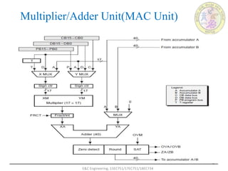
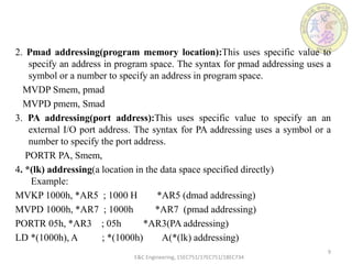
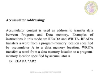
Department of Collegiate and Technical Education
DSPALGORITHM AND ARCHITECTURE
(15EC751/17EC751/18EC734)
Module 3
PROGRAMMABLE DIGITAL SIGNAL
PROCESSORS
SESSION 3
E&C Engineering, 15EC751/17EC751/18EC734
1
 To understand the architecture functional block of
MAC and data addressing modes of TMS320C54xx
processors.
Learning objectives
E&C Engineering, 15EC751/17EC751/18EC734 2
 Functional block of MAC of TMS320C54XX
Data Addressing Modes of TMS320C54xx
Table of Content
E&C Engineering, 15EC751/17EC751/18EC734 3
Multiplier/Adder Unit(MAC Unit)
E&C Engineering, 15EC751/17EC751/18EC734
4
 The kernel of the DSP device architecture is
multiplier/adder unit. The multiplier/adder unit of
TMS320C54xx devices performs 17 x 17 2’s complement
multiplication with a 40-bit addition effectively in a
single instruction cycle.
 In addition to the multiplier and adder, the unit consists of
control logic for integer and fractional computations and a
16-bit temporary storage register, T.
 The compare, select, and store unit (CSSU) is a hardware
unit specifically incorporated to accelerate the
add/compare/select operation
E&C Engineering, 15EC751/17EC751/18EC734
5
 This operation is essential to implement the Viterbi
algorithm used in many signal-processing applications.
 The exponent encoder unit supports the EXP instructions,
which stores in the T register the number of leading
redundant bits of the accumulator content.
 This information is useful while shifting the accumulator
content for the purpose of scaling.
E&C Engineering, 15EC751/17EC751/18EC734
6
Data Addressing Modes of TMS320C54X
Processors
Data addressing modes provide various ways to access operands to execute instructions and place
results in the memory or the registers. The 54XX devices offer seven basic addressing modes
1. Immediate addressing.
2. Absolute addressing.
3. Accumulator addressing.
4. Direct addressing.
5. Indirect addressing.
6. Memory mapped addressing
7. Stack addressing.
E&C Engineering, 15EC751/17EC751/18EC734
7
Immediate addressing:
The instruction contains the specific value of the operand. The operand
can be short (3,5,8 or 9 bit in length) or long (16 bits in length). The
instruction syntax for short operands occupies one memory location
and long operand occupies two memory locations. This addressing
modes can be used to initialize registers and memory locations.
Example: LD #20, DP.
RPT #0FFFFh.
Absolute Addressing:
The instruction contains a specified address in the operand.
1. Dmad addressing (data memory location): This uses specific value
to specify an address in data space. The syntax for dmad addressing
uses a symbol or a number to specify an address in data space.
MVDK Smem,dmad
MVDM dmad,MMR
E&C Engineering, 15EC751/17EC751/18EC734
8
2. Pmad addressing(program memory location):This uses specific value to
specify an address in program space. The syntax for pmad addressing uses a
symbol or a number to specify an address in program space.
MVDP Smem, pmad
MVPD pmem, Smad
3. PA addressing(port address):This uses specific value to specify an an
external I/O port address. The syntax for PA addressing uses a symbol or a
number to specify the port address.
PORTR PA, Smem,
4. *(lk) addressing(a location in the data space specified directly)
Example:
MVKP 1000h, *AR5 ; 1000 H *AR5 (dmad addressing)
MVPD 1000h, *AR7 ; 1000h *AR7 (pmad addressing)
PORTR 05h, *AR3 ; 05h *AR3(PA addressing)
LD *(1000h), A ; *(1000h) A(*(lk) addressing)
E&C Engineering, 15EC751/17EC751/18EC734
9
Accumulator Addressing:
Accumulator content is used as address to transfer data
between Program and Data memory. Examples of
instructions in this mode are READA and WRITA. READA
transfers a word from a program-memory location specified
by accumulator A to a data memory location. WRITA
transfers a word from a data memory location to a program-
memory location specified by accumulator A.
Ex: READA *AR2
E&C Engineering, 15EC751/17EC751/18EC734
10
LEARNING OUTCOME
Able to understand and remember the
architecture functional block of MAC
To understand and remember the addressing
modes of TMS320C54XX device.
E&C Engineering, 15EC751/17EC751/18EC734
11
REFERENCES:
“Digital Signal Processing”, Avatar Singh and S.
Srinivasan, Thomson Learning, 2004.
REFERENCE BOOKS:
1.Digital Signal Processing: A practical approach, Ifeachor
E. C., Jervis B. W Pearson- Education, PHI/ 2002
2.“Digital Signal Processors”, B Venkataramani and M
Bhaskar TMH, 2002
3. “Architectures for Digital Signal Processing”, Peter Pirsch
John Weily, 2007
12
E&C Engineering, 15EC751/17EC751/18EC734
CHAIRMAN : Dr. Rangaraju
H.O.D : Dr Revanna C R
Content Developer: Prof.Hemanth kumar C S
Moderator: Prof.Hemanth Kumar C S
Prof. Roopashree D
13
E&C Engineering, 15EC751/17EC751/18EC734
QUESTIONS ?
14
E&C Engineering, 15EC751/17EC751/18EC734

ECE_18EC734_M3S3.ppt.pptx

  • 1.
    Department of Collegiateand Technical Education DSPALGORITHM AND ARCHITECTURE (15EC751/17EC751/18EC734) Module 3 PROGRAMMABLE DIGITAL SIGNAL PROCESSORS SESSION 3 E&C Engineering, 15EC751/17EC751/18EC734 1
  • 2.
     To understandthe architecture functional block of MAC and data addressing modes of TMS320C54xx processors. Learning objectives E&C Engineering, 15EC751/17EC751/18EC734 2
  • 3.
     Functional blockof MAC of TMS320C54XX Data Addressing Modes of TMS320C54xx Table of Content E&C Engineering, 15EC751/17EC751/18EC734 3
  • 4.
    Multiplier/Adder Unit(MAC Unit) E&CEngineering, 15EC751/17EC751/18EC734 4
  • 5.
     The kernelof the DSP device architecture is multiplier/adder unit. The multiplier/adder unit of TMS320C54xx devices performs 17 x 17 2’s complement multiplication with a 40-bit addition effectively in a single instruction cycle.  In addition to the multiplier and adder, the unit consists of control logic for integer and fractional computations and a 16-bit temporary storage register, T.  The compare, select, and store unit (CSSU) is a hardware unit specifically incorporated to accelerate the add/compare/select operation E&C Engineering, 15EC751/17EC751/18EC734 5
  • 6.
     This operationis essential to implement the Viterbi algorithm used in many signal-processing applications.  The exponent encoder unit supports the EXP instructions, which stores in the T register the number of leading redundant bits of the accumulator content.  This information is useful while shifting the accumulator content for the purpose of scaling. E&C Engineering, 15EC751/17EC751/18EC734 6
  • 7.
    Data Addressing Modesof TMS320C54X Processors Data addressing modes provide various ways to access operands to execute instructions and place results in the memory or the registers. The 54XX devices offer seven basic addressing modes 1. Immediate addressing. 2. Absolute addressing. 3. Accumulator addressing. 4. Direct addressing. 5. Indirect addressing. 6. Memory mapped addressing 7. Stack addressing. E&C Engineering, 15EC751/17EC751/18EC734 7
  • 8.
    Immediate addressing: The instructioncontains the specific value of the operand. The operand can be short (3,5,8 or 9 bit in length) or long (16 bits in length). The instruction syntax for short operands occupies one memory location and long operand occupies two memory locations. This addressing modes can be used to initialize registers and memory locations. Example: LD #20, DP. RPT #0FFFFh. Absolute Addressing: The instruction contains a specified address in the operand. 1. Dmad addressing (data memory location): This uses specific value to specify an address in data space. The syntax for dmad addressing uses a symbol or a number to specify an address in data space. MVDK Smem,dmad MVDM dmad,MMR E&C Engineering, 15EC751/17EC751/18EC734 8
  • 9.
    2. Pmad addressing(programmemory location):This uses specific value to specify an address in program space. The syntax for pmad addressing uses a symbol or a number to specify an address in program space. MVDP Smem, pmad MVPD pmem, Smad 3. PA addressing(port address):This uses specific value to specify an an external I/O port address. The syntax for PA addressing uses a symbol or a number to specify the port address. PORTR PA, Smem, 4. *(lk) addressing(a location in the data space specified directly) Example: MVKP 1000h, *AR5 ; 1000 H *AR5 (dmad addressing) MVPD 1000h, *AR7 ; 1000h *AR7 (pmad addressing) PORTR 05h, *AR3 ; 05h *AR3(PA addressing) LD *(1000h), A ; *(1000h) A(*(lk) addressing) E&C Engineering, 15EC751/17EC751/18EC734 9
  • 10.
    Accumulator Addressing: Accumulator contentis used as address to transfer data between Program and Data memory. Examples of instructions in this mode are READA and WRITA. READA transfers a word from a program-memory location specified by accumulator A to a data memory location. WRITA transfers a word from a data memory location to a program- memory location specified by accumulator A. Ex: READA *AR2 E&C Engineering, 15EC751/17EC751/18EC734 10
  • 11.
    LEARNING OUTCOME Able tounderstand and remember the architecture functional block of MAC To understand and remember the addressing modes of TMS320C54XX device. E&C Engineering, 15EC751/17EC751/18EC734 11
  • 12.
    REFERENCES: “Digital Signal Processing”,Avatar Singh and S. Srinivasan, Thomson Learning, 2004. REFERENCE BOOKS: 1.Digital Signal Processing: A practical approach, Ifeachor E. C., Jervis B. W Pearson- Education, PHI/ 2002 2.“Digital Signal Processors”, B Venkataramani and M Bhaskar TMH, 2002 3. “Architectures for Digital Signal Processing”, Peter Pirsch John Weily, 2007 12 E&C Engineering, 15EC751/17EC751/18EC734
  • 13.
    CHAIRMAN : Dr.Rangaraju H.O.D : Dr Revanna C R Content Developer: Prof.Hemanth kumar C S Moderator: Prof.Hemanth Kumar C S Prof. Roopashree D 13 E&C Engineering, 15EC751/17EC751/18EC734
  • 14.
    QUESTIONS ? 14 E&C Engineering,15EC751/17EC751/18EC734