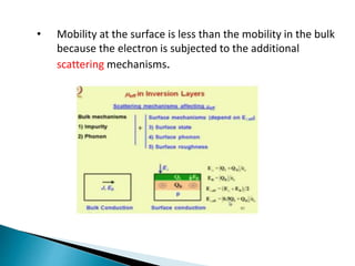
• Mobility at the surface is less than the mobility in the bulk
because the electron is subjected to the additional
scattering mechanisms.
 The surface scattering mechanisms depend on an effective
value of perpendicular electric field.
 So with refers to this diagram , If we call perpendicular as a
field just at the surface of the semiconductor then the effective
value of electric field is less than this value.
 Because not all the carriers over the thickness of the inversion
layer, so the green region here is the inversion layer, so not all
carriers in the thickness of the inversion layer experience the
same value of perpendicular electric field.
 And that is why one has to use an effective electric field or
average electric field that is valid over the entire thickness of the
carriers
 So this is resulting from impurity and phonon scattering in
the bulk of the surface state scattering.
 This is called coulomb scattering because it is because of
coulomb force between the charges and the carriers now.
 On the other hand, what could be called as modern CMOS is
moving towards a right on this graph.
 So 1 micron CMOS you see you are at the borderline here of
surface phonon scattering and surface roughness scattering
and as you move towards the right.
 Another channel length of the CMOS devices decreases the
surface roughness scattering.
 The scattering increases with effective electric field and
therefore they can be clubbed together.
 We neglect the surface coulomb scattering and the result
we can write in the following way so this is the bulk mobility and
the sum total of the scattering again is 1/Mu phonon and
1/scattering roughness both of these scattering mechanisms.
 The scattering increases with effective electric field and
therefore they can be clubbed together. Okay and then there is
a constant of proportionality coming here.
 So the saturation velocity formula there is an
empirical relation. So this it falls with lattice temperature
for silicon this is the relation for gallium arsenide also.
 The saturation velocity falls with temperature
according to this formula now you see that this number10
power 7 is the order of thermal velocity
 The complete field dependent mobility model for silicon ,
there is no velocity overshoot beyond the saturation value so the
smooth curve joining these 2 ends the slope for low values of
Parallel electric field is Mu effective it is a function of the
perpendicular electric field so this line is a straight line Mu effective
into e parallel.
 The complete drift velocity expression is mobility which is a
function of both E parallel and E perpendicular multiplied by the
parallel electric field.
 So there is a so-called free dependent mobility which
depends on both parallel and perpendicular electric fields Mu
effective is m0 when perpendicular electric field effective
value or perpendicular electric field is 0.
 In gallium arsenide the whole mobility is very poor. The
curve rises linearly for small values of E parallel as in the case
of silicon.
DRIFT DIFFUSION TRANSPORT MODEL

DRIFT DIFFUSION TRANSPORT MODEL

  • 2.
    • Mobility atthe surface is less than the mobility in the bulk because the electron is subjected to the additional scattering mechanisms.
  • 3.
     The surfacescattering mechanisms depend on an effective value of perpendicular electric field.  So with refers to this diagram , If we call perpendicular as a field just at the surface of the semiconductor then the effective value of electric field is less than this value.  Because not all the carriers over the thickness of the inversion layer, so the green region here is the inversion layer, so not all carriers in the thickness of the inversion layer experience the same value of perpendicular electric field.  And that is why one has to use an effective electric field or average electric field that is valid over the entire thickness of the carriers
  • 4.
     So thisis resulting from impurity and phonon scattering in the bulk of the surface state scattering.  This is called coulomb scattering because it is because of coulomb force between the charges and the carriers now.
  • 7.
     On theother hand, what could be called as modern CMOS is moving towards a right on this graph.  So 1 micron CMOS you see you are at the borderline here of surface phonon scattering and surface roughness scattering and as you move towards the right.  Another channel length of the CMOS devices decreases the surface roughness scattering.  The scattering increases with effective electric field and therefore they can be clubbed together.
  • 8.
     We neglectthe surface coulomb scattering and the result we can write in the following way so this is the bulk mobility and the sum total of the scattering again is 1/Mu phonon and 1/scattering roughness both of these scattering mechanisms.  The scattering increases with effective electric field and therefore they can be clubbed together. Okay and then there is a constant of proportionality coming here.
  • 9.
     So thesaturation velocity formula there is an empirical relation. So this it falls with lattice temperature for silicon this is the relation for gallium arsenide also.  The saturation velocity falls with temperature according to this formula now you see that this number10 power 7 is the order of thermal velocity
  • 10.
     The completefield dependent mobility model for silicon , there is no velocity overshoot beyond the saturation value so the smooth curve joining these 2 ends the slope for low values of Parallel electric field is Mu effective it is a function of the perpendicular electric field so this line is a straight line Mu effective into e parallel.
  • 11.
     The completedrift velocity expression is mobility which is a function of both E parallel and E perpendicular multiplied by the parallel electric field.  So there is a so-called free dependent mobility which depends on both parallel and perpendicular electric fields Mu effective is m0 when perpendicular electric field effective value or perpendicular electric field is 0.
  • 12.
     In galliumarsenide the whole mobility is very poor. The curve rises linearly for small values of E parallel as in the case of silicon.