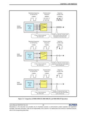
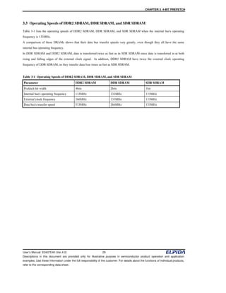
This chapter describes the 4-bit prefetch architecture used in DDR2 SDRAM. The 4-bit prefetch allows the internal bus width to be four times wider than the external bus width, enabling data transfers up to 400Mbps or faster without increasing the internal bus speed. DDR2 SDRAM uses a 4-bit prefetch to allow transferring 4 times as much data per clock cycle compared to DDR SDRAM or SDR SDRAM, operating at twice the external clock frequency of DDR SDRAM for a data transfer rate of 533Mbps even when the internal bus is at 133MHz.