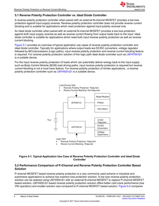
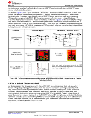
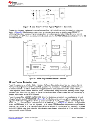
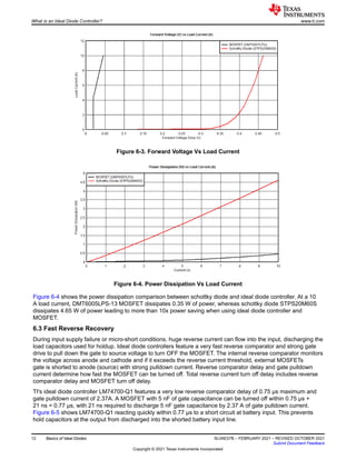
Application Note
Basics of Ideal Diodes
ABSTRACT
Schottky diodes are widely used in power system designs to provide protection from various input supply
fault conditions and to provide system redundancy by paralleling power supplies. Power schottky diodes are
used in automotive power system design to provide protection from reverse battery conditions and protect
from various automotive electrical transients. Industrial systems traditionally have employed schottky diodes to
provide reverse polarity protection from field power supply mis-wiring and provide immunity from lightning and
industrial surges.
Commonly used industrial systems, telecommunication servers, storage, and infrastructure equipments employ
schottky diodes to provide system redundancy or increase power capacity by ORing two or more power sources.
However, the forward voltage drop of the schottky diodes results in significant power loss at high currents and
increases the need for thermal management using heat sinks and a larger PCB space. Forward conduction loss
and associated thermal management reduces efficiency and increases system cost and space. With increasing
system power levels and need for improved power density, schottky diodes are not preferred for newer high
performance system designs.
This application note highlights the limitations of conventional input battery protection solutions using schottky
diodes or P-Channel MOSFETs and discusses how Ideal Diode Controllers from Texas Instruments (TI) can be
used to improve efficiency and performance in battery input protection applications and power supply ORing
applications.
Table of Contents
1 Introduction.............................................................................................................................................................................2
2 Reverse Battery Protection....................................................................................................................................................2
3 ORing Power Supplies........................................................................................................................................................... 4
4 Reverse Battery Protection using MOSFETs....................................................................................................................... 4
5 Reverse Polarity Protection vs Reverse Current Blocking.................................................................................................7
6 What is an Ideal Diode Controller?....................................................................................................................................... 9
7 Automotive Transient protection with Ideal Diode Controllers........................................................................................16
8 ORing Power Supplies with Ideal Diode Controllers.........................................................................................................19
9 Integrated Ideal Diode Solution...........................................................................................................................................22
10 Summary............................................................................................................................................................................. 24
11 References...........................................................................................................................................................................24
12 Revision History................................................................................................................................................................. 24
List of Figures
Figure 2-1. Reversed Connected Battery: Damage to MCU or DC/DC converter.......................................................................3
Figure 2-2. Reversed Connected Battery: Damage to Polarized Capacitors.............................................................................. 3
Figure 2-3. Reverse Battery Protection Using Schottky Diode....................................................................................................3
Figure 2-4. Schottky Diode Response to Reverse Battery Condition..........................................................................................3
Figure 3-1. Diode ORing..............................................................................................................................................................4
Figure 4-1. Reverse Battery Protection using P-Channel MOSFET............................................................................................5
Figure 4-2. Dynamic Reverse Polarity - Schottky Diode..............................................................................................................5
Figure 4-3. Dynamic Reverse Polarity - P-Channel MOSFET.....................................................................................................5
Figure 4-4. Input Short - Schottky Diode..................................................................................................................................... 6
Figure 4-5. Input Short - P-Channel MOSFET.............................................................................................................................6
Figure 4-6. AC Superimposed Test - Schottky Diode.................................................................................................................. 6
Figure 4-7. AC Superimposed Test - P-Channel MOSFET......................................................................................................... 6
Figure 4-8. Reverse Battery Protection Using N-Channel MOSFET...........................................................................................7
www.ti.com Table of Contents
SLVAE57B – FEBRUARY 2021 – REVISED OCTOBER 2021
Submit Document Feedback
Basics of Ideal Diodes 1
Copyright © 2021 Texas Instruments Incorporated
Figure 5-1. Typical Application Use Case of Reverse Polarity Protection Controller and Ideal Diode Controller........................8
Figure 5-2. Performance Comparison of P-channel MOSFET and LM74500-Q1 Based Reverse Polarity Protection
Solution.................................................................................................................................................................................... 9
Figure 6-1. Ideal Diode Controller - Typical Application Schematic........................................................................................... 11
Figure 6-2. Block Diagram of Ideal Diode Controller..................................................................................................................11
Figure 6-3. Forward Voltage Vs Load Current...........................................................................................................................12
Figure 6-4. Power Dissipation Vs Load Current........................................................................................................................ 12
Figure 6-5. Input Short Circuit Response of LM74700-Q1........................................................................................................ 13
Figure 6-6. Fast Load Transient Response of LM74700-Q1..................................................................................................... 14
Figure 6-7. Application Circuit for 200V Unsuppressed Load Dump Protection........................................................................15
Figure 6-8. LM74701-Q1 Operation During VDS Clamp Mode................................................................................................. 16
Figure 7-1. Reverse Battery Protection Using LM74700-Q1..................................................................................................... 16
Figure 7-2. LM74700-Q1 Response to Static Reverse Polarity.................................................................................................17
Figure 7-3. LM74700-Q1 Response to ISO 7637-2 Pulse 1......................................................................................................18
Figure 7-4. LM74700-Q1 Response to Input Micro-short.......................................................................................................... 18
Figure 7-5. LM74700-Q1 AC Superimposed Test......................................................................................................................19
Figure 8-1. Typical OR-ing Application...................................................................................................................................... 20
Figure 8-2. ORing VIN1 to VIN2 Switch Over...............................................................................................................................20
Figure 8-3. ORing VIN1 to VIN2 Switch Over...............................................................................................................................20
Figure 8-4. ORing VIN2 to VIN1 Switch Over...............................................................................................................................21
Figure 8-5. ORing VIN2 to VIN1 Switch Over...............................................................................................................................21
Figure 8-6. ORing - VIN2 Failure and Switch Over to VIN1 ........................................................................................................ 21
Figure 8-7. ORing - VIN2 Failure and Switch Over to VIN1 ........................................................................................................ 21
Figure 9-1. LM66100 Reverse Current Blocking Circuit............................................................................................................ 22
Figure 9-2. Reverse Current Blocking Waveform...................................................................................................................... 22
Figure 9-3. LM66100 ORing Solution........................................................................................................................................ 23
Figure 9-4. LM66100 Switchover from IN1 to IN2..................................................................................................................... 23
List of Tables
Table 6-1. Linear Regulation Control vs. Hysteretic ON/OFF Control....................................................................................... 10
Table 9-1. LM66100 Comparison...............................................................................................................................................23
Trademarks
All trademarks are the property of their respective owners.
1 Introduction
This application report discusses traditional methods using schottky diodes or P-Channel MOSFETs to provide
front-end input protection such as reverse battery protection, reverse current blocking, and protection during
input micro-shorts. Next, the report discusses ORing power supplies to provide supply redundancy and increase
power capacity. The report discusses in detail the drawbacks of existing methods and the benefits of using TI's
Ideal Diode Controllers for input protection and ORing applications.
2 Reverse Battery Protection
In front-end power system designs, modules, or subsystems that directly run from battery power require
protection from reverse battery connection or dynamic reverse polarity conditions during a inductive load
disconnect from the battery. During maintenance of car battery or jump start of the vehicle, the battery can be
connected in reverse polarity during reinstallation and can cause damage to the connected subsystems, circuits,
and components. Figure 2-1 shows a battery that is reverse connected. When this occurs, huge current flows
through ESD diode of micro-controllers, DC/DC converters, or other integrated circuits cause severe damage
to battery connected subsystems. Polarized components such as electrolytic capacitors can be damaged by
reverse connected battery as shown in Figure 2-2.
Trademarks www.ti.com
2 Basics of Ideal Diodes SLVAE57B – FEBRUARY 2021 – REVISED OCTOBER 2021
Submit Document Feedback
Copyright © 2021 Texas Instruments Incorporated
Load
ESD Diode of MCU
or DC-DC Converter
Figure 2-1. Reversed Connected Battery: Damage
to MCU or DC/DC converter
Load
Electrolytic
Capacitor at input
of DC-DC Converter
Figure 2-2. Reversed Connected Battery: Damage
to Polarized Capacitors
Passenger cars and commercial vehicles are fitted with 12-V or 24-V battery and the subsystems powered
through the 12-V or 24-V battery are subjected to various electrical transients on their power supply lines
during the operating life time of the vehicle. Automotive EMC testing standards such as ISO 7637-2 and ISO
16750-2, among others, specify electrical transients, test methods, and classify functional performance for
immunity against the specified transients. Reverse battery protection solution is expected to protect the electrical
subsystems from the transients and meet the functional performance status required for each subsystem.
Traditionally, schottky diodes are used to provide reverse battery protection and prevent damage to battery
connected subsystems.
2.1 Reverse Battery Protection with Schottky Diode
The simplest method of reverse battery protection is to add a series diode at input of the system power path.
Figure 2-3 shows a reverse battery protection using a schottky diode. When the battery is installed correctly, load
current flows in the forward direction of the diode. If the battery is installed with the wrong polarity, the diode is
reverse biased and blocks reverse current, thereby protecting the load from negative voltage.
Figure 2-4 shows the response to a reverse polarity condition at the input. When the 12 V input is quickly
reversed to -20 V, the output voltage remains without collapsing immediately or following the negative input as
the schottky diode gets reverse biased and isolates the output from negative voltage. A bulk capacitor placed
at the output holds the output from falling immediately and can supply the load for a short time before the input
supply recovers.
Load
VBAT VOUT
Figure 2-3. Reverse Battery Protection Using
Schottky Diode
Figure 2-4. Schottky Diode Response to Reverse
Battery Condition
Drawbacks of using schottky diode for reverse battery protection include:
• Power dissipation: Forward conduction results in significant efficiency loss at higher load currents.
• Thermal management: Heat sink is needed to manage power dissipation, increasing cost and space.
• Reverse leakage current: Reverse leakage current of high voltage schottky diodes increase dramatically with
junction temperature, resulting in higher power dissipation during reverse conduction.
www.ti.com Reverse Battery Protection
SLVAE57B – FEBRUARY 2021 – REVISED OCTOBER 2021
Submit Document Feedback
Basics of Ideal Diodes 3
Copyright © 2021 Texas Instruments Incorporated
• Head room for downstream power converter: During a cold start of the car, the battery voltage drops as low
as 3 V or 4 V during a warm start. Forward voltage drop reduces subsequent power converter head-room and
a wider operating power converter is required to work during 3 V or 4 V cold crank operation. This requires a
wider VIN range DC/DC boost converter to be used after the diode.
On systems where large holdup capacitors are used, inrush current during startup can be huge and must not
exceed the maximum diode current. This needs to be considered when choosing thermal layout or heat sink.
3 ORing Power Supplies
Schottky diodes are traditionally used to OR two or more power supplies to increase system redundancy or
increase power capacity in N+1 configuration. Typically more than one power supply units (PSU) are paralleled
using schottky diodes in a N+1 redundant configuration. Minimum 'N' supplies are required to power the load
and additional supply unit is provided for redundancy in case of a single point failure: one power supply unit fails.
Power supply with higher voltage provides most or all of the power required by the load. To share loads almost
equally among the power supplies, power supply DC set point is adjusted to match other units closely.
Load
GND
Power Supply 1
Power Supply 2
Figure 3-1. Diode ORing
Figure 3-1 shows dual ORing scheme where two PSUs power the load through two schottky diodes. When one
of the power supply fails and its input is shorted, schottky diode in its path is reverse biased and isolates the
other power supply from the failure. Load remains fully powered from the working power supply until the faulty
unit is replaced.
Load Sharing: Load sharing between two power supplies is mainly dependent on the forward voltage difference
of the schottky diodes and voltage difference between two power supplies. Power supply with higher voltage and
lower forward voltage schottky diode carries most of the current. Forward voltage drop of the schottky diode has
a negative temperature co-efficient and it reduces with increasing temperature. This can lead to situation where
a single supply carries the entire load current though second supply is still present and results in increased
junction temperature TJ. This necessitates a careful heat sink design and thermal management between two
diodes.
Power Dissipation and Thermal Management: Apart from the key concerns such as power dissipation and
the associated thermal management, reverse leakage current at a higher temperature can result in efficiency
loss and lead to thermal run away situations if thermal design is not done properly. Reverse leakage current
of high voltage schottky diodes increase drastically with temperature. For example, 60 V rated schottky diode
STPS20M60S has a 100 mA reverse leakage current at 150 °C, which amounts to 6 W of power dissipation at
-60 V. Consider a case when only one power supply is fully supplying the load current due to forward voltage
difference of schottky diodes or offset in power supply DC set point. If this first power supply fails, the second
supply takes over and supplies the entire load, but the schottky diode of the first one had a higher TJ before
turning off and conducts large reverse leakage current. This can lead to a thermal run-away situation where
the schottky continues to conduct increased reverse current and gets damaged. A damaged schottky diode and
failed power supply can pull down the entire power system leading to a system failure. Even if thermal run-away
is avoided by careful heat sink design, sustained power dissipation in the reverse conduction results in unwanted
power loss.
4 Reverse Battery Protection using MOSFETs
In this section, reverse battery protection using P-Channel MOSFETs and N-Channel MOSFETs are discussed
along with the benefits and drawbacks.
ORing Power Supplies www.ti.com
4 Basics of Ideal Diodes SLVAE57B – FEBRUARY 2021 – REVISED OCTOBER 2021
Submit Document Feedback
Copyright © 2021 Texas Instruments Incorporated
4.1 Reverse Battery Protection using P-Channel MOSFET
The schottky diode can be replaced with a P-Channel MOSFET to provide reverse battery protection as shown
in Figure 4-1. The forward drop of the diode can be reduced by replacing the schottky diode with a P-channel
MOSFET and its body diode oriented in the same direction as the schottky diode. During normal operation of the
battery, the body diode from MOSFET is forward biased and conducts for a very short time until the MOSFET is
turned ON when gate voltage is pulled below source. When the battery polarity is reversed, gate-source voltage
swings positive and the MOSFET is turned off, protecting the downstream circuits from negative voltage.
Load
VBAT VOUT
Figure 4-1. Reverse Battery Protection using P-Channel MOSFET
During dynamic reverse polarity where input quickly swings negative from positive, the P-Channel MOSFET is
turned OFF when the input starts going negative because the gate-source voltage swings positive. Further note
that the output also reaches close to or a diode drop lower than the system ground and protects the downstream
DC/DC converters from negative voltage. The holdup capacitors are discharged as this P-Channel MOSFET
protection does not block reverse current from flowing back into the input. An additional circuit can be added to
sense the voltage difference between the input and output and turn off the MOSFET when the input goes lower
than output, but requires increased cost and board space.
In Figure 4-3, the P-Channel MOSFET circuit protects the output from dynamic reverse polarity condition where
the input quickly changes from 12 V to -20 V. Output remains protected from the negative voltage after the initial
reverse voltage for 50 µs. Note that the output is completely discharged due to lack of reverse current blocking
functionality and any hold up capacitors are discharged.
Figure 4-2. Dynamic Reverse Polarity - Schottky
Diode
Figure 4-3. Dynamic Reverse Polarity - P-Channel
MOSFET
4.2 Input Short or supply interruption
Figure 4-4 and Figure 4-5 show the performance comparison of P-Channel MOSFET with a schottky diode
during an input short or interruption. During an input short, the schottky diode is quickly reverse biased and
blocks reverse current from flowing back into the shorted input. Output is isolated from the input short and hold
www.ti.com Reverse Battery Protection using MOSFETs
SLVAE57B – FEBRUARY 2021 – REVISED OCTOBER 2021
Submit Document Feedback
Basics of Ideal Diodes 5
Copyright © 2021 Texas Instruments Incorporated
capacitors at the output provide back-up power to the load, leading to droop in the output voltage. When the
input short is removed, load is powered through the schottky diode.
In Figure 4-5, P-Channel MOSFET turns off when the gate-source voltage crosses VTH of MOSFET, close to 0 V.
Output voltage sees a huge drop due to lack of reverse current blocking functionality.
Figure 4-4. Input Short - Schottky Diode Figure 4-5. Input Short - P-Channel MOSFET
4.3 Diode Rectification During Line Disturbance
In automotive systems, the battery line is subjected to various disturbances and transients during normal
operation of the vehicle. One of the key tests is the supply line disturbance called AC superimposed test where
AC disturbance with 2 V - 4 V peak to peak and 20 Hz to 30 KHz is applied on the battery supply line and the
subsystems are expected to run without any functionality loss.
The schottky diode rectifies the AC line disturbance by blocking the reverse current. Figure 4-6 shows the
rectified output and input current which has the AC component added due to the injected AC line disturbance.
Power dissipation on the schottky diode increases due to the increased RMS current multiplied by the forward
drop. This additional heat needs to be managed for reliable operation during the AC superimposed test.
Figure 4-6. AC Superimposed Test - Schottky
Diode
Figure 4-7. AC Superimposed Test - P-Channel
MOSFET
Figure 4-7 shows the performance of P-Channel MOSFET circuit. Since the P-Channel MOSFET does not block
reverse current, rectification of the line disturbance does not happen and this results in increased RMS input
current. Power dissipation on the MOSFET may not be a major concern due to the low forward voltage drop as
the MOSFET remains on, however, the RMS current of output electrolytic capacitors due to its ESR produces
Reverse Battery Protection using MOSFETs www.ti.com
6 Basics of Ideal Diodes SLVAE57B – FEBRUARY 2021 – REVISED OCTOBER 2021
Submit Document Feedback
Copyright © 2021 Texas Instruments Incorporated
additional heat on the capacitors. To prevent damage to the capacitors due to overheating, required capacitance
can be split into multiple parallel capacitors to reduce the ESR. This adds to the system cost and space.
Rectification is possible by adding reverse current blocking functionality using an external comparator based
methods, but this increases cost and space.
4.4 Reverse Battery Protection using N-Channel MOSFET
An alternate method of reverse battery protection is using an N-Channel MOSFET on the low side, such as
the ground return path. The operating principle is similar to the P-Channel MOSFET in Figure 4-1. During
normal operation, the body diode of the MOSFET is forward biased and conducts until the MOSFET is turned
ON. MOSFET is turned ON quickly as the battery input charges the gate through the current limiting resistors.
MOSFET turns OFF during static reverse battery or dynamic reverse battery conditions after the battery input
starts to swing negative, as the gate-source voltage starts to go below MOSFET Vth and swings negative.
Load
VBAT VOUT
Figure 4-8. Reverse Battery Protection Using N-Channel MOSFET
Section 4.1 describes the performance during the dynamic reverse polarity is similar to the P-Channel MOSFET
solution. However, a jump in the system ground voltage during turn ON/OFF or load current transients may not
be tolerated by all systems and needs to be considered during system designs.
5 Reverse Polarity Protection vs Reverse Current Blocking
Reverse battery protection involves two aspects of protection, commonly referred to as reverse polarity
protection (RPP) and reverse current blocking (RCB). Reverse polarity protection, also referred to as reverse
hookup protection (RHP), prevents the load from getting damaged due to negative voltage at the input during
a reversely connected battery or dynamic reverse polarity conditions during a inductive load disconnect from
battery. Reverse polarity protection does not necessarily block reverse current flowing into the battery from
the load or downstream DC/DC converters. In many automotive subsystems, large holdup capacitors are used
to provide sufficient back up power during a short interruption of battery line or shorted battery input, so that
the subsystem can function uninterrupted or perform maintenance housekeeping tasks such as memory dump
before turning off. Reverse current blocking prevents reverse current from flowing back into the battery from the
load and allows holdup capacitors to provide additional back up time for the subsystem to function during various
dynamic reverse battery conditions or short interruptions.
One key difference between battery protection using schottky diode and protection using P-Channel MOSFET is
the schottky diode blocks reverse current flowing from the load back into the battery all the time and inherently
provides both reverse polarity protection and reverse current blocking. When the battery is connected with
its terminal reversed, the schottky diode gets reverse biased and blocks reverse current from discharging the
holdup capacitors connected to the load. This naturally isolates the load from the negative input voltage and
provides reverse polarity protection to the load.
The battery protection shown in Figure 4-1 or in Figure 4-8 does not block reverse current from flowing back into
the battery since the MOSFETs are turned off when the battery voltage is close the Vth of the MOSFETs and not
as soon as the battery voltage starts to drop. During a input micro-short at the battery, holdup capacitors can be
discharged to a voltage lower than the downstream DC/DC converters UVLO, leading to reset of the subsystem.
www.ti.com Reverse Battery Protection using MOSFETs
SLVAE57B – FEBRUARY 2021 – REVISED OCTOBER 2021
Submit Document Feedback
Basics of Ideal Diodes 7
Copyright © 2021 Texas Instruments Incorporated
5.1 Reverse Polarity Protection Controller vs. Ideal Diode Controller
A reverse polarity protection controller when paired with an external N-channel MOSFET provides a low loss
protection against input supply reversal. Reverse polarity protection controller does not provide reverse current
blocking and is suitable for applications which need protection against input polarity reversal only.
An ideal diode controller when paired with an external N-channel MOSFET provides a low loss protection
against both input supply reversal as well as reverse current flowing from output loads back to the input. Ideal
diode controller is suitable for applications which need both input reverse polarity protection as well as reverse
current blocking.
Figure 5-1 provides an overview of typical application use cases of reverse polarity protection controller and
ideal diode controller. Typically for applications where output loads are DC/DC converters, voltage regulator
followed by MCU/processors (Logic paths), input reverse polarity protection and reverse current blocking feature
is required. For reverse polarity protection solution of the logic path ideal diode controller such as LM74700-Q1
is a suitable device.
For the input reverse polarity protection of loads which can potentially deliver energy back to the input supply
such as Body Control Module (BCM) load driving paths, input reverse polarity protection is required but reverse
current blocking is not a must have feature. For reverse polarity protection of similar applications , a reverse
polarity protection controller such as LM74500-Q1 is a suitable device.
LM74700-Q1
VBAT
Load Driving Path
x Reverse Polarity Protection: Required
x Revere Current Blocking: Not Required
LM74500-Q1
Linear
Regulator
DC/DC
Converters
Voltage
Supervisors
Wiper/Washer
Relays
Horn/Alarm
Logic Path
x Reverse Polarity Protection: Required
x Revere Current Blocking: Required
Figure 5-1. Typical Application Use Case of Reverse Polarity Protection Controller and Ideal Diode
Controller
5.2 Performance Comparison of P-Channel and Reverse Polarity Protection Controller Based
Solution
P-channel MOSFET based reverse polarity protection is a very commonly used scheme in industrial and
automotive applications to achieve low insertion loss protection solution. A low loss reverse polarity protection
solution can be realized using LM74500-Q1 with an external N-channel MOSFET to replace P-channel MOSFET
based solution. LM74500-Q1 based reverse polarity protection solution offers better cold crank performance (low
VIN operation) and smaller solution size compared to P-channel MOSFET based solution. Figure 5-2 compares
Reverse Polarity Protection vs Reverse Current Blocking www.ti.com
8 Basics of Ideal Diodes SLVAE57B – FEBRUARY 2021 – REVISED OCTOBER 2021
Submit Document Feedback
Copyright © 2021 Texas Instruments Incorporated
the performance benefits of LM74500-Q1 + N-channel MOSFET over traditional P-channel MOSFET based
reverse polarity protection solution.
As shown in Figure 5-2, for a given power level LM74500-Q1+ N-channel MOSFET solution can be three times
smaller than a similar power rated P-channel MOSFET solution. Also as P-channel MOSFET is self biased
by simply pulling it's gate pin low and thus P-channel MOSFET shows poorer cold crank performance (low
VIN operation) compared to LM74500-Q1. During severe cold crank where battery voltage falls below 4 V,
P-channel MOSFET series resistance increases drastically as shown in Figure 5-2. This leads to higher voltage
drop across the P-channel MOSFET. Also with higher gate to source threshold (VT) this can sometimes lead to
system reset due to turning off of the P-channel MOSFET. On the other side, LM74500-Q1 has excellent severe
cold crank performance. LM74500-Q1 keeps external FET completely enhanced even when input voltage falls to
3.2 V during severe cold crank operation.
VBATT
LM74500-Q1
GATE
EN
SOURCE
VCAP
GND
TVS
CVCAP
CIN COUT
VOUT
D1
VBATT
COUT
P-channel MOSFET LM74500-Q1 + N-channel MOSFET
VOUT
TVS
R1
CIN
Parameter
Typical Application
Diagram
Solution Size
(Load current >6A)
Low VIN / Cold-Crank
Performance
12mm x 11.7mm
(140mm2
)
7mm x 5.3mm
(37.1mm2
)
Better cold crank performance compared to PFET
based solution. External N-FET remains fully enhanced
even if input voltage falls to 3.2V.
Figure 5-2. Performance Comparison of P-channel MOSFET and LM74500-Q1 Based Reverse Polarity
Protection Solution
6 What is an Ideal Diode Controller?
An ideal diode controller drives an external N-channel MOSFET to emulate an ideal diode with a very low
forward voltage drop and negligible reverse current. Key features such as low operating quiescent current,
very low shutdown current, regulated forward voltage, and fast reverse current response enable ideal diode
controllers to emulate an ideal diode in variety of applications. The power MOSFET is connected in such
way that its body diode blocks reverse current when the MOSFET is turned OFF. Forward voltage drop and
power dissipation are reduced significantly as the MOSFET is turned ON during forward conduction. Ideal diode
controllers sense the reverse current through MOSFET and turn it OFF, allowing the body diode to block reverse
current. Ideal diode controllers can be classified into two types based on the gate control mechanism: Linear
Regulation Control and Hysteretic ON/OFF Control.
www.ti.com What is an Ideal Diode Controller?
SLVAE57B – FEBRUARY 2021 – REVISED OCTOBER 2021
Submit Document Feedback
Basics of Ideal Diodes 9
Copyright © 2021 Texas Instruments Incorporated
6.1 Linear Regulation Control Vs Hysteretic ON/OFF Control
In linear regulation control, forward voltage of the MOSFET is regulated by controlling the gate voltage based on
the load current. Linear regulation is achieved by controlling the gate voltage and thereby varying the RDS(ON)
of the MOSFET based on load current. At nominal load currents, gate-source voltage is maintained above
the MOSFETs Vth and at lower load currents, gate-source voltage is maintained close to MOSFETs Vth with
increased RDS(ON). At higher load currents, gate-source voltage is parked close to the maximum gate drive
voltage, operating close to lowest possible RDS(ON). Choosing the MOSFET based on the operating power
requirements helps maintain the MOSFET under regulation during most of the load conditions. Linear regulation
of the forward voltage along with a fast reverse current blocking helps ensure zero DC current flows back into
the input. Further, it also minimizes the peak reverse current during a input supply failure, input supply transients
or input supply droop.
In Hysteretic ON/OFF control, MOSFET is fully turned ON when the forward turn ON comparator threshold
VFWD_ON is exceeded and turned OFF when the reverse comparator threshold VREV_OFF is reached. When the
MOSFET is ON, the gate is fully enhanced and the gate-source voltage is not controlled depending on the load
current. MOSFET is turned off when the reverse current reaches VREV_OFF / RDS(ON). Note that the MOSFET
cannot turn OFF if a reverse current less than VREV_OFF / RDS(ON) flows. The reverse turn off threshold VREV_OFF
is fixed negative value or programmable allowing small positive value. In ideal diode controllers where the
reverse comparator threshold is programmable and can be set to a small positive value, the DC reverse current
can be completely blocked. Additionally, setting the reverse comparator threshold to a small positive value can
require a minimum forward load current VREV_OFF / RDS(ON) to turn ON the MOSFET. If a minimum forward load
current is not maintained, MOSFET can turn ON/OFF continuously leading to sustained oscillation of the gate
voltage.
Table 6-1. Linear Regulation Control vs. Hysteretic ON/OFF Control
IDEAL DIODE
CONTROLLER
OPERATING RANGE (ABSOLUTE
MAXIMUM RATINGS)
LINEAR REGULATION CONTROL HYSTERETIC ON/OFF CONTROL
LM74700-Q1 ±65 V Yes No
LM74610-Q1 ±45 V No Yes
LM5050-1 and
LM5050-1-Q1
±100 V Yes No
LM5050-2 ±100 V Yes No
TPS2410 and
TPS2412
±18 V Yes No
TPS2411 and
TPS2413
±18 V No Yes
TPS2419 ±18 V No Yes
LM74701-Q1 ±65 V Yes No
LM7472x-Q1 ±70 V Yes No
LM74800-Q1 and
LM74810-Q1
±70 V Yes No
LM74801-Q1 ±70 V No Yes
A typical application schematic in Figure 6-1 shows the LM74700-Q1 ideal diode controller driving an external
N-Channel MOSFET. MOSFET is connected with its source tied to the input so that body diode blocks the
reverse current when turned OFF. The charge pump capacitor is connected between Anode and VCAP to
provide sufficient gate drive voltage to turn on the MOSFET. EN pin is used to turn the MOSFET ON, providing
regulated low forward drop across anode to cathode during normal operation. Pulling down the EN pin turns OFF
the MOSFET and the controller goes into low shutdown current mode. When the MOSFET is turned OFF, the
load can still draw power through body diode of the MOSFET.
What is an Ideal Diode Controller? www.ti.com
10 Basics of Ideal Diodes SLVAE57B – FEBRUARY 2021 – REVISED OCTOBER 2021
Submit Document Feedback
Copyright © 2021 Texas Instruments Incorporated
LM74700
GATE CATHODE
EN
ANODE
VCAP
GND
VBATT
TVS
Voltage
Regulator
VOUT
ON OFF
Figure 6-1. Ideal Diode Controller - Typical Application Schematic
This section discusses the key performance features of the LM74700-Q1 using the functional block diagram
shown in Figure 6-2. Ideal diode controllers have an internal charge pump to drive the gate of MOSFET
sufficiently higher than anode during normal operation, forward comparator to turn ON and reverse current
comparator to turn OFF when reverse current is detected, allowing the MOSFET body diode to block reverse DC
current completely.
VANODE
Charge Pump
Enable Logic
VANODE
VCAP
VCAP
+
±
Q
R
S Q
+
±
+
±
+
±
GM AMP
+
±
+
±
20 mV
50 mV
-11 mV
VCAP
COMPARATOR
COMPARATOR
VCAP_UV
VCAP_UV
ENABLE LOGIC
ENGATE
GATE DRIVER
ENABLE
LOGIC
REVERSE
PROTECTION
LOGIC
VANODE
Bias Rails VANODE
ANODE GATE CATHODE
VCAP_UV
VANODE
VCAP EN GND
Charge
Pump
Figure 6-2. Block Diagram of Ideal Diode Controller
6.2 Low Forward Conduction Loss
Forward voltage drop of schottky diodes increases the forward conduction power loss and requires thermal
management using heat sink and requires PCB space leading to increased cost. Ideal diode controllers use
an external MOSFET to reduce the forward voltage to 20 mV or lower, depending on the control scheme.
Linear regulation control scheme maintains 20 mV forward voltage during most of the operating current range.
Hysteretic ON/OFF control fully enhances the MOSFET to reduce the forward voltage and the forward drop is
decided solely based on the MOSFET used.
Forward voltage of the MOSFET DMT6007LFG driven by ideal diode controller is compared against forward
voltage of schottky diode STPS20M60S in Figure 6-3. An ideal diode controller using linear regulation scheme
regulates the forward voltage to low 20 mV up to load current = 20 mV / RDS(MIN) and load current higher than
20 mV / RDS(MIN) forward voltage solely depends on MOSFETs RRD(ON). In Figure 6-3, MOSFET is regulated to
20 mV forward voltage up to 5.7 A and beyond 5.7, a MOSFET is fully enhanced and forward voltage increases
based on load current. At 10 A, low forward voltage drop is reduced to 35 mV against 465 mV using a Schottky
diode. LM74722-Q1 ideal diode controller offers an even lower forward voltage drop of 13 mV, providing further
improvement in power efficiency.
www.ti.com What is an Ideal Diode Controller?
SLVAE57B – FEBRUARY 2021 – REVISED OCTOBER 2021
Submit Document Feedback
Basics of Ideal Diodes 11
Copyright © 2021 Texas Instruments Incorporated
Figure 6-3. Forward Voltage Vs Load Current
Figure 6-4. Power Dissipation Vs Load Current
Figure 6-4 shows the power dissipation comparison between schottky diode and ideal diode controller. At a 10
A load current, DMT6005LPS-13 MOSFET dissipates 0.35 W of power, whereas schottky diode STPS20M60S
dissipates 4.65 W of power leading to more than 10x power saving when using ideal diode controller and
MOSFET.
6.3 Fast Reverse Recovery
During input supply failure or micro-short conditions, huge reverse current can flow into the input, discharging the
load capacitors used for holdup. Ideal diode controllers feature a very fast reverse comparator and strong gate
drive to pull down the gate to source voltage to turn OFF the MOSFET. The internal reverse comparator monitors
the voltage across anode and cathode and if it exceeds the reverse current threshold, external MOSFETs
gate is shorted to anode (source) with strong pulldown current. Reverse comparator delay and gate pulldown
current determine how fast the MOSFET can be turned off. Total reverse current turn off delay includes reverse
comparator delay and MOSFET turn off delay.
TI's ideal diode controller LM74700-Q1 features a very low reverse comparator delay of 0.75 µs maximum and
gate pulldown current of 2.37A. A MOSFET with 5 nF of gate capacitance can be turned off within 0.75 µs +
21 ns = 0.77 µs, with 21 ns required to discharge 5 nF gate capacitance by 2.37 A of gate pulldown current.
Figure 6-5 shows LM74700-Q1 reacting quickly within 0.77 µs to a short circuit at battery input. This prevents
hold capacitors at the output from discharged into the shorted battery input line.
What is an Ideal Diode Controller? www.ti.com
12 Basics of Ideal Diodes SLVAE57B – FEBRUARY 2021 – REVISED OCTOBER 2021
Submit Document Feedback
Copyright © 2021 Texas Instruments Incorporated
VOUT
VBATT
IBATT
VGATE
Figure 6-5. Input Short Circuit Response of LM74700-Q1
6.4 Very Low Shutdown Current
In automotive applications, very low shutdown current is a requirement to meet the overall system requirement
of less than 100 µA where many battery powered subsystems co-exist. TI's ideal diode controller LM74700-Q1
features a very low shutdown current of 1.5 µA maximum to meet the automotive system requirements. This also
helps many other battery powered or energy harvesting applications where low shutdown current is preferred.
6.5 Fast Load Transient Response
Ideal diode controllers operating with linear regulation control scheme maintain low forward voltage by controlling
the gate-source voltage depending on load current. Gate-source voltage is lower at light load conditions and
increases as the load current increases. While linear regulation scheme helps achieve zero DC reverse current,
it can be disadvantageous to have low gate-source voltage during a sudden load transient from light load to
heavy load. At lighter loads, gate-source voltage is operated just above Vth of MOSFET and the RDS(ON) is
higher (than nominal) to meet to forward regulation, RDS(ON)_LIGHT_LOAD = 20 mV / ILIGHT_LOAD. When the load
suddenly changes from light load to higher loads, the gate of the MOSFET needs to quickly charge from lower
voltage to higher voltage to meet the sudden increased load demand. If the gate is not quickly charged, output
voltage sees a worst case voltage drop equal to IHEAVY_LOAD × RDS(ON)_LIGHT_LOAD, but not more than MOSFETs
body diode drop. In many ORing applications this droop in output voltage may not be acceptable as this reduces
the headroom of power supply downstream.
TI's ideal diode controller LM74700-Q1 features 11 mA peak source current when forward drop exceeds 50
mV. This feature helps in quickly charging the gate during fast load transient minimizing supply voltage droop.
Figure 6-6 shows the load transient response of the LM74700-Q1 when load changes from 10 mA light load to
5 A suddenly. Output voltage drop is minimized to <50 mV as the controller quickly reacts and enhances the
MOSFETs gate quickly.
www.ti.com What is an Ideal Diode Controller?
SLVAE57B – FEBRUARY 2021 – REVISED OCTOBER 2021
Submit Document Feedback
Basics of Ideal Diodes 13
Copyright © 2021 Texas Instruments Incorporated
Figure 6-6. Fast Load Transient Response of LM74700-Q1
6.6 Additional Features in Ideal Diode Controllers
In addition to the features discussed above, ideal diode controllers can also support multiple other features like
over voltage protection, inrush current control, TVS less operation. These features are explained in detail the
sections below.
6.6.1 Back-to-Back FET Driving Ideal Diode Controllers
Ideal Diode controllers such as LM7480-Q1 and LM7472x-Q1 can drive and control external back to back
N-Channel MOSFETs to emulate an ideal diode rectifier with power path ON/OFF control, inrush current limiting
and over voltage protection. Load disconnection during an overvoltage fault such as load-dump allows use of low
voltage downstream components, enabling dense ECU designs such as ADAS camera, USB Hubs, LIDAR, and
TCU. LM7480x-Q1 and LM7472x-Q1 have separate GATE controls for ideal diode control and ON/OFF control.
Automotive ECU designs powered from a vehicle battery need to be load dump tolerant. For the 12-V car
battery based designs, the suppressed load dump peak specification is 35-V. For the system designs without
the centralized load dump suppression, the surge voltage due to unsuppressed load dump can peak up to 101
V in 12-V systems and 202 V in 24-V battery based systems as per the ISO-16750-2 standard. Conventional
solutions use several high-power TVS stacks (SMD sized) to clamp to a safe level (below the downstream
absolute maximum voltages) during the unsuppressed load dump resulting in an increase in overall solution size
and BoM cost of the front-end protection circuit.
The LM7480-Q1 controller with the external MOSFETs configured in common source topology as shown in
Figure 6-7 below provides unsuppressed load dump protection.
What is an Ideal Diode Controller? www.ti.com
14 Basics of Ideal Diodes SLVAE57B – FEBRUARY 2021 – REVISED OCTOBER 2021
Submit Document Feedback
Copyright © 2021 Texas Instruments Incorporated
GND
DGATE
A
HGATE C
VOUT
LM74800-Q1
VS
R1
D3
CAP
OUT
VBATT: 24V with
200V Load Dump
C1
R2
R1
OV
EN/UVLO
VSNS
SW
ON OFF
VOUT
VOUT
Output Clamp
OV Cut-off
Q1
D1
Q2
C2
D2
200V 60V
Figure 6-7. Application Circuit for 200V Unsuppressed Load Dump Protection
6.6.2 Very Low Quiescent Current
For battery-operated electronic systems in automotive applications, battery supply remains on even when
ignition is off, to support features like remote key entry and security which are required even in ignition-off
state. To maximize battery life, there is a need for power protection solutions to provide robust reverse protection
while maintaining low supply current.
In an automotive system, the low IQ during sleep mode/ignition off state is generally achieved by following
approaches:
1. An external IGN connection is commonly found in redundant supply input-based ECU designs. Such a
design uses extra wiring to the ECU.
2. An internal control signal from micro controller is used to pull EN low to disable the device. If the digital and
power sections of the design are far apart or on separate boards, this signal becomes prone to noise and
unknown state, making the overall operation unreliable.
LM7472x-Q1 devices enable <35uA quiescent current without dependency on MCU EN control signal or an
external signal through a wire, making the device more suitable in comparison.
6.6.3 TVSless Operation
The increase in processing power levels and miniaturized electronic system sizes has increased the demand
for high efficiency and high power density designs. This poses new challenges for system designers particularly
in designing automotive front-end protection systems. Devices such as LM74701-Q1 and LM74721-Q1 enable
a smaller solution size and lower cost, making these devices suitable for designing input reverse polarity
protection of space constrained applications such as ADAS camera modules. These devices use integrated
active clamping to limit the input voltage levels during negative transient pulses. When the voltage across Drain
and Source of the external MOSFET reaches VDSCLAMP level, the external MOSFET is operated in saturation
region, operating as an active clamp element and dissipates transient pulse energy of events such as ISO7637-2
pulse 1 negative transient. During the VDS clamp operation device allows flow of reverse current from output
capacitor back to the input source. VDS clamp threshold is selected such that it does not engage into VDS
clamp mode for automotive EMC tests where reverse current blocking is needed such as AC superimpose
performance (LV124,E-06, ISO16750-2) and Input micro short interruption events (LV124, E-10) ensuring robust
EMC performance. For further details on how to design input-side TVS-less reverse polarity protection solution,
refer to data sheet LM74701-Q1
www.ti.com What is an Ideal Diode Controller?
SLVAE57B – FEBRUARY 2021 – REVISED OCTOBER 2021
Submit Document Feedback
Basics of Ideal Diodes 15
Copyright © 2021 Texas Instruments Incorporated
VOUT
COUT
13.5V +
-
VCLAMP
- (VCLAMP ± VOUT)
0V
ISO7637 Pulse 1
VOUT
VIN
13.5V
0V
GND
GATE
ANODE
EN
VIN
SW
LM74701-Q1
R2
R1
BATT_MON
CATHODE
VCAP
ON OFF
CIN
Figure 6-8. LM74701-Q1 Operation During VDS Clamp Mode
In applications such as body control module load driving paths, where input reverse polarity protection is
required but reverse current blocking is not a must-have requirement, LM74501-Q1 enables TVSless operation
using a gate discharge timer feature, offering space and price advantages. For further details, refer to LM74501
data sheet.
7 Automotive Transient protection with Ideal Diode Controllers
Ideal diode controllers drive external N-channel MOSFETs to emulate ideal diodes. As described earlier, ideal
diode controllers have a built-in charge pump to drive the gate of MOSFET sufficiently higher than anode during
normal operation and reverse current comparator to turn off when reverse current is detected, allowing the
MOSFET body diode to block reverse current completely. This enables the ideal diode controllers to be used in
reverse battery protection.
7.1 LM74700-Q1 with N-Channel MOSFET
Figure 7-1 shows a typical 12 V reverse battery protection circuit using the LM74700-Q1. The MOSFET body
diode is oriented correctly to block reverse current flowing back in to the battery when the LM74700 is turned off.
When battery power is applied through anode, body diode of the MOSFET initially conducts before the MOSFET
is turned on. During startup, when the anode voltage reaches POR threshold, the internal charge pump turns
on and starts to drive the gate of MOSFET higher than the anode (source of MOSFET), thereby turning on the
MOSFET. If the battery is installed with reverse polarity or wired incorrectly during maintenance or repair, the
MOSFET is off already and body diode of the MOSFET blocks reverse current. This prevents negative voltage
from appearing on the output and protects the downstream circuit from damage.
LM74700
GATE CATHODE
EN
ANODE
VCAP
GND
VBATT
TVS
Voltage
Regulator
VOUT
ON OFF
Figure 7-1. Reverse Battery Protection Using LM74700-Q1
Automotive Transient protection with Ideal Diode Controllers www.ti.com
16 Basics of Ideal Diodes SLVAE57B – FEBRUARY 2021 – REVISED OCTOBER 2021
Submit Document Feedback
Copyright © 2021 Texas Instruments Incorporated
7.2 Static Reverse Polarity
During maintenance of the car battery or jump start of the vehicle, the battery can be connected in reverse
polarity during reinstallation. When the battery is connected with reversed polarity, the LM74700-Q1 remains
turned off to protect the downstream circuits and components from damage. In Figure 7-2, output voltage
remains protected when a reverse battery connection of -12 V is applied at its input.
OUTPUT REMAINS PROTECTED
FROM NEGATIVE VOLTAGE
Figure 7-2. LM74700-Q1 Response to Static Reverse Polarity
7.3 Dynamic Reverse Polarity
During dynamic reverse polarity conditions specified in ISO 7637-2 Pulse 1, negative transient voltage as low as
-150 V is applied at the 12-V battery supply line with 10-Ω generator impedance for 2 ms and -600 V at the 24-V
battery supply line with 50-Ω generator impedance for 1 ms. Figure 7-3 shows the response of the LM74700-Q1
to ISO 7637-2 Pulse 1 applied at the input. Before the test pulse is applied, the MOSFET is ON and allows the
load current to pass through. When the ISO 7637-2 test pulse 1 is applied at the battery input, the load current
starts to reverse quickly and tries to pull the output voltage negative. LM74700-Q1 detects the reverse current
and turns OFF the MOSFET within 0.75 µs to block reverse current and prevents the output from going negative.
Generally, bulk holdup capacitors are used after the ideal diode circuit provides energy to rest of the module
during such transients. The LM74700-Q1 turns off the MOSFET quickly within 0.75 µs to prevent discharge of
the bulk holdup capacitors. Note that the input TVS is required to clamp the voltage from exceeding the absolute
maximum ratings of LM74700-Q1 and MOSFET.
www.ti.com Automotive Transient protection with Ideal Diode Controllers
SLVAE57B – FEBRUARY 2021 – REVISED OCTOBER 2021
Submit Document Feedback
Basics of Ideal Diodes 17
Copyright © 2021 Texas Instruments Incorporated
VOUT
VGATE
VIN
IIN
TVS CLAMPING AT -42V
GATE TURNS OFF QUICKLY WITHIN 1…s
Figure 7-3. LM74700-Q1 Response to ISO 7637-2 Pulse 1
7.4 Input Micro-Short
Many power systems are required to withstand short interruption in supply line or input micro-short and continue
to function uninterrupted. In Figure 7-4, when the input micro-short is applied at the input, the LM74700-Q1
reacts quickly to turn off the MOSFET to block reverse current from flowing back into the shorted supply. Output
remains ON during the input short as the output hold-up capacitors are isolated from input short and supply load
current until the input recovers from micro-short. Note that after the MOSFET is turned off, input current rings
due to the parasitic inductance in the supply path and does not contribute to reverse current.
MOSFET turned off quickly
within 1 …s: VGS = 0V
Reverse Current is
blocked within 1 …s
Ringing due to parasitic source
inductance, not reverse current
Output remains ON during input short
MOSFET is turned back ON after
the input short is removed
Figure 7-4. LM74700-Q1 Response to Input Micro-short
7.5 Diode Rectification of Supply Line disturbance
Fast reverse current blocking and fast reverse recovery capability of Ideal Diode Controllers help in active
rectification of the AC disturbance by turning on and off every cycle. The Ideal Diode controller detects reverse
current flowing back into the supply during the test and turns OFF the GATE quickly thereby reducing the
Automotive Transient protection with Ideal Diode Controllers www.ti.com
18 Basics of Ideal Diodes SLVAE57B – FEBRUARY 2021 – REVISED OCTOBER 2021
Submit Document Feedback
Copyright © 2021 Texas Instruments Incorporated
RMS value of input current by half. Power dissipation in the MOSFET during the test is reduced due to low
forward voltage drop. Figure 7-5 shows the performance of LM74700-Q1 during supply line disturbance or the
AC superimposed test.
Reverse Current is
blocked every cycle
RMS Current is
reduced by half due
to rectification
Gate turns off every cycle to block reverse current
Figure 7-5. LM74700-Q1 AC Superimposed Test
Faster turn on and turn off speed of ideal diode gate drivers such as that of LM7472x-Q1, enables active
rectification during AC superimpose scenario defined by ISO16750 and LV124, E-06 tests. Active rectification
during AC superimpose performance results in lower ripple current and thus enables low power loss across
external MOSFET and output electrolytic capacitors.
In the design of mild-hybrid vehicle power trees, the frequency applied during ACS can be up to 200 KHz so
as to tailor it to the ripple of the craw-pole Lundell alternator. Hence, the protection device used with DC-DC
converters need to be insensitive to frequencies up to 200KHz. Key performance features such as very low
forward voltage drop, fast gate drive, fast reverse recovery response and integrated boost converter enables the
LM74722-Q1 ideal diode controller to achieve active rectification of AC voltage ripple up to 200 kHz.
8 ORing Power Supplies with Ideal Diode Controllers
The LM74700-Q1 combined with external N-Channel MOSFETs can be used in OR-ing Solution as shown in
Figure 8-1. The forward diode drop is reduced as the external N-Channel MOSFET is turned ON during normal
operation. The LM74700-Q1 quickly detects the reverse current and quickly pulls down the MOSFET gate,
leaving the body diode of the MOSFET to block the reverse current flow.
www.ti.com ORing Power Supplies with Ideal Diode Controllers
SLVAE57B – FEBRUARY 2021 – REVISED OCTOBER 2021
Submit Document Feedback
Basics of Ideal Diodes 19
Copyright © 2021 Texas Instruments Incorporated
VIN1
LOAD
VOUT
COUT
LM74700
GATE CATHODE
EN
ANODE
VCAP
GND
VIN2
LM74700
GATE CATHODE
EN
ANODE
VCAP
GND
Figure 8-1. Typical OR-ing Application
An effective OR-ing solution needs to be extremely fast to limit the reverse current amount and duration.
The LM74700-Q1 devices in an OR-ing configuration constantly sense the voltage difference between anode
and cathode pins, which are the voltage levels at the power sources (VIN1, VIN2) and the common load point
respectively. The source to drain voltage VDS of the MOSFET is monitored by the anode and cathode pins of
the LM74700-Q1. A fast comparator shuts down the gate drive through a fast pulldown within 0.75 μs (typical)
as soon as V(IN) – V(OUT) falls below –11 mV. It turns on the gate with 11 mA gate charge current once the
differential forward voltage V(IN) – V(OUT) exceeds 50 mV.
VIN1
VGATE1
IIN1
VOUT
VOUT SWITCHES to VIN2 15 V
Time (5 ms/DIV)
Figure 8-2. ORing VIN1 to VIN2 Switch Over
VIN1
VGATE1
IIN2
VOUT
VIN2 SUPPLIES LOAD CURRENT
VOUT SWITCHES to VIN2 15V
Time (5 ms/DIV)
Figure 8-3. ORing VIN1 to VIN2 Switch Over
ORing Power Supplies with Ideal Diode Controllers www.ti.com
20 Basics of Ideal Diodes SLVAE57B – FEBRUARY 2021 – REVISED OCTOBER 2021
Submit Document Feedback
Copyright © 2021 Texas Instruments Incorporated
VIN1
VGATE1
IIN1
VOUT VOUT SWITCHES to VIN1: 12V
Time (5 ms/DIV)
Figure 8-4. ORing VIN2 to VIN1 Switch Over
VIN1
VGATE1
IIN2
VOUT
VOUT SWITCHES to VIN1: 12V
VIN1 SUPPLIES LOAD CURRENT
Time (5 ms/DIV)
Figure 8-5. ORing VIN2 to VIN1 Switch Over
VIN1
VOUT
VGATE1
IIN1
Time (5 ms/DIV)
Figure 8-6. ORing - VIN2 Failure and Switch Over to
VIN1
VOUT
VIN1
VIN2
IIN2
Time (10 ms/DIV)
Figure 8-7. ORing - VIN2 Failure and Switch Over to
VIN1
Figure 8-2 to Figure 8-5 show the smooth switch over between two power supply rails VIN1 at 12 V and VIN2
at 15 V. Figure 8-6 and Figure 8-7 illustrate the performance when VIN2 fails. The LM74700-Q1 controlling VIN2
power rail turns off quickly, so that the output remains uninterrupted and VIN1 is protected from VIN2 failure.
Power dissipation and its associated thermal management issues of using a schottky diode are minimized due
to the low forward voltage drop of ideal diode controllers. MOSFETs do not have leakage currents as high as
a schottky diode at high temperatures and using MOSFETs reduces the reverse leakage loss. This improves
overall efficiency and reliability of the system.
Load sharing concerns due to schottky diode difference in forward voltage and its negative temperature co-
efficient are not present when using ideal diode controllers. Further, the linear regulation of forward voltage drop
enhances load sharing between power supplies.
www.ti.com ORing Power Supplies with Ideal Diode Controllers
SLVAE57B – FEBRUARY 2021 – REVISED OCTOBER 2021
Submit Document Feedback
Basics of Ideal Diodes 21
Copyright © 2021 Texas Instruments Incorporated
9 Integrated Ideal Diode Solution
For lower voltage applications, such as backup battery solutions, an integrated ideal diode solution can be used.
The LM66100 uses a P-channel MOSFET and integrates the functionality of an ideal diode into a single device.
A typical application schematic in Figure 9-1 shows the LM66100 ideal diode in a reverse current blocking (RCB)
circuit. The chip enable works by comparing the CE pin voltage to the input voltage. When the CE pin voltage
is higher than VIN, the device is disabled and the PMOS is turned off. When the CE pin voltage is lower than
VIN, then the MOSFET is on and the device operates with low forward voltage drop. By connecting the CE
pin to VOUT in this configuration, this ensures that the MOSFET is disabled whenever the output voltage is
forced higher than the input voltage. The LM66100 integrated ideal diode also integrates reverse polarity/battery
protection, which helps to prevent damage to the upstream battery if it is wired incorrectly.
Figure 9-1. LM66100 Reverse Current Blocking Circuit
Figure 9-2. Reverse Current Blocking Waveform
Similar to the ideal diode controllers, the LM66100 can also be used in redundant power architectures for ORing
between power supplies. By using two LM66100s with the CE pins tied to the other input voltage channel. This
ensures that the highest input supply voltage is selected as the output. Since the highest supply is always be
selected, the solution allows for a make-before-break configuration, which prevents any reverse current flow
between the input supplies.
Integrated Ideal Diode Solution www.ti.com
22 Basics of Ideal Diodes SLVAE57B – FEBRUARY 2021 – REVISED OCTOBER 2021
Submit Document Feedback
Copyright © 2021 Texas Instruments Incorporated
Figure 9-3. LM66100 ORing Solution
Figure 9-4 shows a typical switchover event from VIN1 to VIN2. During this switchover event, VIN1 decays
causing the LM66100 to switch to VIN2, while blocking reverse current from entering VIN1.
Figure 9-4. LM66100 Switchover from IN1 to IN2
The LM66100 integrated ideal diode also contains the same advantages as the ideal diode controllers, when
compared to a discrete diode or FET solution. During normal operation, the LM66100 has a lower forward
conduction loss when compared to a discrete diode. Instead of operating with the normal 0.3 V–0.4 V drop of a
discrete diode, the power loss across the LM66100 is minimized across the MOSFET instead. This results in a
lower power dissipation, leading to a higher power savings for applications.
The LM66100 also has a fast reverse voltage recovery time when compared to a discrete FET. While a discrete
FET does not turn off until the voltage drops below the VTH of the FET, the LM66100 stops reverse current
within tOFF once the voltage on the output rises above the input. This helps prevent output capacitors from
discharging current back into the upstream supply, which can damage components such as input batteries or
PSUs.
Table 9-1. LM66100 Comparison
FEATURE IDEAL DIODE CONTROLLER LM66100
DISCRETE
DIODE
DISCRETE FET
Low Power
Dissipation
✓ ✓ ✓
Low Reverse
Leakage
Current
✓ ✓ ✓
Reverse
Polarity
Protection
✓ ✓ ✓ *(additional components)*
www.ti.com Integrated Ideal Diode Solution
SLVAE57B – FEBRUARY 2021 – REVISED OCTOBER 2021
Submit Document Feedback
Basics of Ideal Diodes 23
Copyright © 2021 Texas Instruments Incorporated
10 Summary
This application note discusses the benefits of using Texas Instruments ideal diode controllers in reverse battery
protection and ORing applications. The report discusses performance of the LM74700-Q1 Ideal diode controller
during front-end input protection tests such as dynamic reverse polarity, input micro-short, and power line
disturbance and compares it to existing methods. Key features such as low forward conduction loss, fast reverse
recovery, true reverse current blocking, and fast load transient response enables the ideal diode controller
LM74700-Q1 to provide more efficient and robust reverse battery protection.
Key benefits such as low forward conduction loss, reduced leakage, and simplified load sharing enables the
ideal diode controller to OR power supplies more efficiently and reliably.
11 References
• Texas Instruments, LM74700-Q1 Low IQ Reverse Battery Protection Ideal Diode Controller data sheet.
• Texas Instruments, Reverse Current / Battery Protection Circuits application note.
• Texas Instruments, Full Featured N+1 and ORing Power Rail Controller data sheet.
12 Revision History
NOTE: Page numbers for previous revisions may differ from page numbers in the current version.
Changes from Revision A (February 2021) to Revision B (October 2021) Page
• Updated table with new devices....................................................................................................................... 10
• Updated low forward conduction loss with enhancement in forward voltage obtained using LM7472x-Q1..... 11
• Added Back-to-Back FET Driving Ideal Diode Controllers topic.......................................................................14
• Added Very Low Quiescent Current topic.........................................................................................................15
• Added new TVSless Operation topic................................................................................................................15
• Updated topic to include performance enhancement obtained using LM7472x...............................................18
Changes from Revision * (May 2019) to Revision A (February 2021) Page
• Added Reverse Polarity Protection Controller vs. Ideal Diode Controller section.............................................. 8
• Added Performance Comparison of P-Channel and Reverse Polarity Protection Controller Based Solution
section................................................................................................................................................................ 8
Summary www.ti.com
24 Basics of Ideal Diodes SLVAE57B – FEBRUARY 2021 – REVISED OCTOBER 2021
Submit Document Feedback
Copyright © 2021 Texas Instruments Incorporated
IMPORTANT NOTICE AND DISCLAIMER
TI PROVIDES TECHNICAL AND RELIABILITY DATA (INCLUDING DATA SHEETS), DESIGN RESOURCES (INCLUDING REFERENCE
DESIGNS), APPLICATION OR OTHER DESIGN ADVICE, WEB TOOLS, SAFETY INFORMATION, AND OTHER RESOURCES “AS IS”
AND WITH ALL FAULTS, AND DISCLAIMS ALL WARRANTIES, EXPRESS AND IMPLIED, INCLUDING WITHOUT LIMITATION ANY
IMPLIED WARRANTIES OF MERCHANTABILITY, FITNESS FOR A PARTICULAR PURPOSE OR NON-INFRINGEMENT OF THIRD
PARTY INTELLECTUAL PROPERTY RIGHTS.
These resources are intended for skilled developers designing with TI products. You are solely responsible for (1) selecting the appropriate
TI products for your application, (2) designing, validating and testing your application, and (3) ensuring your application meets applicable
standards, and any other safety, security, regulatory or other requirements.
These resources are subject to change without notice. TI grants you permission to use these resources only for development of an
application that uses the TI products described in the resource. Other reproduction and display of these resources is prohibited. No license
is granted to any other TI intellectual property right or to any third party intellectual property right. TI disclaims responsibility for, and you
will fully indemnify TI and its representatives against, any claims, damages, costs, losses, and liabilities arising out of your use of these
resources.
TI’s products are provided subject to TI’s Terms of Sale or other applicable terms available either on ti.com or provided in conjunction with
such TI products. TI’s provision of these resources does not expand or otherwise alter TI’s applicable warranties or warranty disclaimers for
TI products.
TI objects to and rejects any additional or different terms you may have proposed. IMPORTANT NOTICE
Mailing Address: Texas Instruments, Post Office Box 655303, Dallas, Texas 75265
Copyright © 2022, Texas Instruments Incorporated

DIODOSAA.pdf

  • 1.
    Application Note Basics ofIdeal Diodes ABSTRACT Schottky diodes are widely used in power system designs to provide protection from various input supply fault conditions and to provide system redundancy by paralleling power supplies. Power schottky diodes are used in automotive power system design to provide protection from reverse battery conditions and protect from various automotive electrical transients. Industrial systems traditionally have employed schottky diodes to provide reverse polarity protection from field power supply mis-wiring and provide immunity from lightning and industrial surges. Commonly used industrial systems, telecommunication servers, storage, and infrastructure equipments employ schottky diodes to provide system redundancy or increase power capacity by ORing two or more power sources. However, the forward voltage drop of the schottky diodes results in significant power loss at high currents and increases the need for thermal management using heat sinks and a larger PCB space. Forward conduction loss and associated thermal management reduces efficiency and increases system cost and space. With increasing system power levels and need for improved power density, schottky diodes are not preferred for newer high performance system designs. This application note highlights the limitations of conventional input battery protection solutions using schottky diodes or P-Channel MOSFETs and discusses how Ideal Diode Controllers from Texas Instruments (TI) can be used to improve efficiency and performance in battery input protection applications and power supply ORing applications. Table of Contents 1 Introduction.............................................................................................................................................................................2 2 Reverse Battery Protection....................................................................................................................................................2 3 ORing Power Supplies........................................................................................................................................................... 4 4 Reverse Battery Protection using MOSFETs....................................................................................................................... 4 5 Reverse Polarity Protection vs Reverse Current Blocking.................................................................................................7 6 What is an Ideal Diode Controller?....................................................................................................................................... 9 7 Automotive Transient protection with Ideal Diode Controllers........................................................................................16 8 ORing Power Supplies with Ideal Diode Controllers.........................................................................................................19 9 Integrated Ideal Diode Solution...........................................................................................................................................22 10 Summary............................................................................................................................................................................. 24 11 References...........................................................................................................................................................................24 12 Revision History................................................................................................................................................................. 24 List of Figures Figure 2-1. Reversed Connected Battery: Damage to MCU or DC/DC converter.......................................................................3 Figure 2-2. Reversed Connected Battery: Damage to Polarized Capacitors.............................................................................. 3 Figure 2-3. Reverse Battery Protection Using Schottky Diode....................................................................................................3 Figure 2-4. Schottky Diode Response to Reverse Battery Condition..........................................................................................3 Figure 3-1. Diode ORing..............................................................................................................................................................4 Figure 4-1. Reverse Battery Protection using P-Channel MOSFET............................................................................................5 Figure 4-2. Dynamic Reverse Polarity - Schottky Diode..............................................................................................................5 Figure 4-3. Dynamic Reverse Polarity - P-Channel MOSFET.....................................................................................................5 Figure 4-4. Input Short - Schottky Diode..................................................................................................................................... 6 Figure 4-5. Input Short - P-Channel MOSFET.............................................................................................................................6 Figure 4-6. AC Superimposed Test - Schottky Diode.................................................................................................................. 6 Figure 4-7. AC Superimposed Test - P-Channel MOSFET......................................................................................................... 6 Figure 4-8. Reverse Battery Protection Using N-Channel MOSFET...........................................................................................7 www.ti.com Table of Contents SLVAE57B – FEBRUARY 2021 – REVISED OCTOBER 2021 Submit Document Feedback Basics of Ideal Diodes 1 Copyright © 2021 Texas Instruments Incorporated
  • 2.
    Figure 5-1. TypicalApplication Use Case of Reverse Polarity Protection Controller and Ideal Diode Controller........................8 Figure 5-2. Performance Comparison of P-channel MOSFET and LM74500-Q1 Based Reverse Polarity Protection Solution.................................................................................................................................................................................... 9 Figure 6-1. Ideal Diode Controller - Typical Application Schematic........................................................................................... 11 Figure 6-2. Block Diagram of Ideal Diode Controller..................................................................................................................11 Figure 6-3. Forward Voltage Vs Load Current...........................................................................................................................12 Figure 6-4. Power Dissipation Vs Load Current........................................................................................................................ 12 Figure 6-5. Input Short Circuit Response of LM74700-Q1........................................................................................................ 13 Figure 6-6. Fast Load Transient Response of LM74700-Q1..................................................................................................... 14 Figure 6-7. Application Circuit for 200V Unsuppressed Load Dump Protection........................................................................15 Figure 6-8. LM74701-Q1 Operation During VDS Clamp Mode................................................................................................. 16 Figure 7-1. Reverse Battery Protection Using LM74700-Q1..................................................................................................... 16 Figure 7-2. LM74700-Q1 Response to Static Reverse Polarity.................................................................................................17 Figure 7-3. LM74700-Q1 Response to ISO 7637-2 Pulse 1......................................................................................................18 Figure 7-4. LM74700-Q1 Response to Input Micro-short.......................................................................................................... 18 Figure 7-5. LM74700-Q1 AC Superimposed Test......................................................................................................................19 Figure 8-1. Typical OR-ing Application...................................................................................................................................... 20 Figure 8-2. ORing VIN1 to VIN2 Switch Over...............................................................................................................................20 Figure 8-3. ORing VIN1 to VIN2 Switch Over...............................................................................................................................20 Figure 8-4. ORing VIN2 to VIN1 Switch Over...............................................................................................................................21 Figure 8-5. ORing VIN2 to VIN1 Switch Over...............................................................................................................................21 Figure 8-6. ORing - VIN2 Failure and Switch Over to VIN1 ........................................................................................................ 21 Figure 8-7. ORing - VIN2 Failure and Switch Over to VIN1 ........................................................................................................ 21 Figure 9-1. LM66100 Reverse Current Blocking Circuit............................................................................................................ 22 Figure 9-2. Reverse Current Blocking Waveform...................................................................................................................... 22 Figure 9-3. LM66100 ORing Solution........................................................................................................................................ 23 Figure 9-4. LM66100 Switchover from IN1 to IN2..................................................................................................................... 23 List of Tables Table 6-1. Linear Regulation Control vs. Hysteretic ON/OFF Control....................................................................................... 10 Table 9-1. LM66100 Comparison...............................................................................................................................................23 Trademarks All trademarks are the property of their respective owners. 1 Introduction This application report discusses traditional methods using schottky diodes or P-Channel MOSFETs to provide front-end input protection such as reverse battery protection, reverse current blocking, and protection during input micro-shorts. Next, the report discusses ORing power supplies to provide supply redundancy and increase power capacity. The report discusses in detail the drawbacks of existing methods and the benefits of using TI's Ideal Diode Controllers for input protection and ORing applications. 2 Reverse Battery Protection In front-end power system designs, modules, or subsystems that directly run from battery power require protection from reverse battery connection or dynamic reverse polarity conditions during a inductive load disconnect from the battery. During maintenance of car battery or jump start of the vehicle, the battery can be connected in reverse polarity during reinstallation and can cause damage to the connected subsystems, circuits, and components. Figure 2-1 shows a battery that is reverse connected. When this occurs, huge current flows through ESD diode of micro-controllers, DC/DC converters, or other integrated circuits cause severe damage to battery connected subsystems. Polarized components such as electrolytic capacitors can be damaged by reverse connected battery as shown in Figure 2-2. Trademarks www.ti.com 2 Basics of Ideal Diodes SLVAE57B – FEBRUARY 2021 – REVISED OCTOBER 2021 Submit Document Feedback Copyright © 2021 Texas Instruments Incorporated
  • 3.
    Load ESD Diode ofMCU or DC-DC Converter Figure 2-1. Reversed Connected Battery: Damage to MCU or DC/DC converter Load Electrolytic Capacitor at input of DC-DC Converter Figure 2-2. Reversed Connected Battery: Damage to Polarized Capacitors Passenger cars and commercial vehicles are fitted with 12-V or 24-V battery and the subsystems powered through the 12-V or 24-V battery are subjected to various electrical transients on their power supply lines during the operating life time of the vehicle. Automotive EMC testing standards such as ISO 7637-2 and ISO 16750-2, among others, specify electrical transients, test methods, and classify functional performance for immunity against the specified transients. Reverse battery protection solution is expected to protect the electrical subsystems from the transients and meet the functional performance status required for each subsystem. Traditionally, schottky diodes are used to provide reverse battery protection and prevent damage to battery connected subsystems. 2.1 Reverse Battery Protection with Schottky Diode The simplest method of reverse battery protection is to add a series diode at input of the system power path. Figure 2-3 shows a reverse battery protection using a schottky diode. When the battery is installed correctly, load current flows in the forward direction of the diode. If the battery is installed with the wrong polarity, the diode is reverse biased and blocks reverse current, thereby protecting the load from negative voltage. Figure 2-4 shows the response to a reverse polarity condition at the input. When the 12 V input is quickly reversed to -20 V, the output voltage remains without collapsing immediately or following the negative input as the schottky diode gets reverse biased and isolates the output from negative voltage. A bulk capacitor placed at the output holds the output from falling immediately and can supply the load for a short time before the input supply recovers. Load VBAT VOUT Figure 2-3. Reverse Battery Protection Using Schottky Diode Figure 2-4. Schottky Diode Response to Reverse Battery Condition Drawbacks of using schottky diode for reverse battery protection include: • Power dissipation: Forward conduction results in significant efficiency loss at higher load currents. • Thermal management: Heat sink is needed to manage power dissipation, increasing cost and space. • Reverse leakage current: Reverse leakage current of high voltage schottky diodes increase dramatically with junction temperature, resulting in higher power dissipation during reverse conduction. www.ti.com Reverse Battery Protection SLVAE57B – FEBRUARY 2021 – REVISED OCTOBER 2021 Submit Document Feedback Basics of Ideal Diodes 3 Copyright © 2021 Texas Instruments Incorporated
  • 4.
    • Head roomfor downstream power converter: During a cold start of the car, the battery voltage drops as low as 3 V or 4 V during a warm start. Forward voltage drop reduces subsequent power converter head-room and a wider operating power converter is required to work during 3 V or 4 V cold crank operation. This requires a wider VIN range DC/DC boost converter to be used after the diode. On systems where large holdup capacitors are used, inrush current during startup can be huge and must not exceed the maximum diode current. This needs to be considered when choosing thermal layout or heat sink. 3 ORing Power Supplies Schottky diodes are traditionally used to OR two or more power supplies to increase system redundancy or increase power capacity in N+1 configuration. Typically more than one power supply units (PSU) are paralleled using schottky diodes in a N+1 redundant configuration. Minimum 'N' supplies are required to power the load and additional supply unit is provided for redundancy in case of a single point failure: one power supply unit fails. Power supply with higher voltage provides most or all of the power required by the load. To share loads almost equally among the power supplies, power supply DC set point is adjusted to match other units closely. Load GND Power Supply 1 Power Supply 2 Figure 3-1. Diode ORing Figure 3-1 shows dual ORing scheme where two PSUs power the load through two schottky diodes. When one of the power supply fails and its input is shorted, schottky diode in its path is reverse biased and isolates the other power supply from the failure. Load remains fully powered from the working power supply until the faulty unit is replaced. Load Sharing: Load sharing between two power supplies is mainly dependent on the forward voltage difference of the schottky diodes and voltage difference between two power supplies. Power supply with higher voltage and lower forward voltage schottky diode carries most of the current. Forward voltage drop of the schottky diode has a negative temperature co-efficient and it reduces with increasing temperature. This can lead to situation where a single supply carries the entire load current though second supply is still present and results in increased junction temperature TJ. This necessitates a careful heat sink design and thermal management between two diodes. Power Dissipation and Thermal Management: Apart from the key concerns such as power dissipation and the associated thermal management, reverse leakage current at a higher temperature can result in efficiency loss and lead to thermal run away situations if thermal design is not done properly. Reverse leakage current of high voltage schottky diodes increase drastically with temperature. For example, 60 V rated schottky diode STPS20M60S has a 100 mA reverse leakage current at 150 °C, which amounts to 6 W of power dissipation at -60 V. Consider a case when only one power supply is fully supplying the load current due to forward voltage difference of schottky diodes or offset in power supply DC set point. If this first power supply fails, the second supply takes over and supplies the entire load, but the schottky diode of the first one had a higher TJ before turning off and conducts large reverse leakage current. This can lead to a thermal run-away situation where the schottky continues to conduct increased reverse current and gets damaged. A damaged schottky diode and failed power supply can pull down the entire power system leading to a system failure. Even if thermal run-away is avoided by careful heat sink design, sustained power dissipation in the reverse conduction results in unwanted power loss. 4 Reverse Battery Protection using MOSFETs In this section, reverse battery protection using P-Channel MOSFETs and N-Channel MOSFETs are discussed along with the benefits and drawbacks. ORing Power Supplies www.ti.com 4 Basics of Ideal Diodes SLVAE57B – FEBRUARY 2021 – REVISED OCTOBER 2021 Submit Document Feedback Copyright © 2021 Texas Instruments Incorporated
  • 5.
    4.1 Reverse BatteryProtection using P-Channel MOSFET The schottky diode can be replaced with a P-Channel MOSFET to provide reverse battery protection as shown in Figure 4-1. The forward drop of the diode can be reduced by replacing the schottky diode with a P-channel MOSFET and its body diode oriented in the same direction as the schottky diode. During normal operation of the battery, the body diode from MOSFET is forward biased and conducts for a very short time until the MOSFET is turned ON when gate voltage is pulled below source. When the battery polarity is reversed, gate-source voltage swings positive and the MOSFET is turned off, protecting the downstream circuits from negative voltage. Load VBAT VOUT Figure 4-1. Reverse Battery Protection using P-Channel MOSFET During dynamic reverse polarity where input quickly swings negative from positive, the P-Channel MOSFET is turned OFF when the input starts going negative because the gate-source voltage swings positive. Further note that the output also reaches close to or a diode drop lower than the system ground and protects the downstream DC/DC converters from negative voltage. The holdup capacitors are discharged as this P-Channel MOSFET protection does not block reverse current from flowing back into the input. An additional circuit can be added to sense the voltage difference between the input and output and turn off the MOSFET when the input goes lower than output, but requires increased cost and board space. In Figure 4-3, the P-Channel MOSFET circuit protects the output from dynamic reverse polarity condition where the input quickly changes from 12 V to -20 V. Output remains protected from the negative voltage after the initial reverse voltage for 50 µs. Note that the output is completely discharged due to lack of reverse current blocking functionality and any hold up capacitors are discharged. Figure 4-2. Dynamic Reverse Polarity - Schottky Diode Figure 4-3. Dynamic Reverse Polarity - P-Channel MOSFET 4.2 Input Short or supply interruption Figure 4-4 and Figure 4-5 show the performance comparison of P-Channel MOSFET with a schottky diode during an input short or interruption. During an input short, the schottky diode is quickly reverse biased and blocks reverse current from flowing back into the shorted input. Output is isolated from the input short and hold www.ti.com Reverse Battery Protection using MOSFETs SLVAE57B – FEBRUARY 2021 – REVISED OCTOBER 2021 Submit Document Feedback Basics of Ideal Diodes 5 Copyright © 2021 Texas Instruments Incorporated
  • 6.
    capacitors at theoutput provide back-up power to the load, leading to droop in the output voltage. When the input short is removed, load is powered through the schottky diode. In Figure 4-5, P-Channel MOSFET turns off when the gate-source voltage crosses VTH of MOSFET, close to 0 V. Output voltage sees a huge drop due to lack of reverse current blocking functionality. Figure 4-4. Input Short - Schottky Diode Figure 4-5. Input Short - P-Channel MOSFET 4.3 Diode Rectification During Line Disturbance In automotive systems, the battery line is subjected to various disturbances and transients during normal operation of the vehicle. One of the key tests is the supply line disturbance called AC superimposed test where AC disturbance with 2 V - 4 V peak to peak and 20 Hz to 30 KHz is applied on the battery supply line and the subsystems are expected to run without any functionality loss. The schottky diode rectifies the AC line disturbance by blocking the reverse current. Figure 4-6 shows the rectified output and input current which has the AC component added due to the injected AC line disturbance. Power dissipation on the schottky diode increases due to the increased RMS current multiplied by the forward drop. This additional heat needs to be managed for reliable operation during the AC superimposed test. Figure 4-6. AC Superimposed Test - Schottky Diode Figure 4-7. AC Superimposed Test - P-Channel MOSFET Figure 4-7 shows the performance of P-Channel MOSFET circuit. Since the P-Channel MOSFET does not block reverse current, rectification of the line disturbance does not happen and this results in increased RMS input current. Power dissipation on the MOSFET may not be a major concern due to the low forward voltage drop as the MOSFET remains on, however, the RMS current of output electrolytic capacitors due to its ESR produces Reverse Battery Protection using MOSFETs www.ti.com 6 Basics of Ideal Diodes SLVAE57B – FEBRUARY 2021 – REVISED OCTOBER 2021 Submit Document Feedback Copyright © 2021 Texas Instruments Incorporated
  • 7.
    additional heat onthe capacitors. To prevent damage to the capacitors due to overheating, required capacitance can be split into multiple parallel capacitors to reduce the ESR. This adds to the system cost and space. Rectification is possible by adding reverse current blocking functionality using an external comparator based methods, but this increases cost and space. 4.4 Reverse Battery Protection using N-Channel MOSFET An alternate method of reverse battery protection is using an N-Channel MOSFET on the low side, such as the ground return path. The operating principle is similar to the P-Channel MOSFET in Figure 4-1. During normal operation, the body diode of the MOSFET is forward biased and conducts until the MOSFET is turned ON. MOSFET is turned ON quickly as the battery input charges the gate through the current limiting resistors. MOSFET turns OFF during static reverse battery or dynamic reverse battery conditions after the battery input starts to swing negative, as the gate-source voltage starts to go below MOSFET Vth and swings negative. Load VBAT VOUT Figure 4-8. Reverse Battery Protection Using N-Channel MOSFET Section 4.1 describes the performance during the dynamic reverse polarity is similar to the P-Channel MOSFET solution. However, a jump in the system ground voltage during turn ON/OFF or load current transients may not be tolerated by all systems and needs to be considered during system designs. 5 Reverse Polarity Protection vs Reverse Current Blocking Reverse battery protection involves two aspects of protection, commonly referred to as reverse polarity protection (RPP) and reverse current blocking (RCB). Reverse polarity protection, also referred to as reverse hookup protection (RHP), prevents the load from getting damaged due to negative voltage at the input during a reversely connected battery or dynamic reverse polarity conditions during a inductive load disconnect from battery. Reverse polarity protection does not necessarily block reverse current flowing into the battery from the load or downstream DC/DC converters. In many automotive subsystems, large holdup capacitors are used to provide sufficient back up power during a short interruption of battery line or shorted battery input, so that the subsystem can function uninterrupted or perform maintenance housekeeping tasks such as memory dump before turning off. Reverse current blocking prevents reverse current from flowing back into the battery from the load and allows holdup capacitors to provide additional back up time for the subsystem to function during various dynamic reverse battery conditions or short interruptions. One key difference between battery protection using schottky diode and protection using P-Channel MOSFET is the schottky diode blocks reverse current flowing from the load back into the battery all the time and inherently provides both reverse polarity protection and reverse current blocking. When the battery is connected with its terminal reversed, the schottky diode gets reverse biased and blocks reverse current from discharging the holdup capacitors connected to the load. This naturally isolates the load from the negative input voltage and provides reverse polarity protection to the load. The battery protection shown in Figure 4-1 or in Figure 4-8 does not block reverse current from flowing back into the battery since the MOSFETs are turned off when the battery voltage is close the Vth of the MOSFETs and not as soon as the battery voltage starts to drop. During a input micro-short at the battery, holdup capacitors can be discharged to a voltage lower than the downstream DC/DC converters UVLO, leading to reset of the subsystem. www.ti.com Reverse Battery Protection using MOSFETs SLVAE57B – FEBRUARY 2021 – REVISED OCTOBER 2021 Submit Document Feedback Basics of Ideal Diodes 7 Copyright © 2021 Texas Instruments Incorporated
  • 8.
    5.1 Reverse PolarityProtection Controller vs. Ideal Diode Controller A reverse polarity protection controller when paired with an external N-channel MOSFET provides a low loss protection against input supply reversal. Reverse polarity protection controller does not provide reverse current blocking and is suitable for applications which need protection against input polarity reversal only. An ideal diode controller when paired with an external N-channel MOSFET provides a low loss protection against both input supply reversal as well as reverse current flowing from output loads back to the input. Ideal diode controller is suitable for applications which need both input reverse polarity protection as well as reverse current blocking. Figure 5-1 provides an overview of typical application use cases of reverse polarity protection controller and ideal diode controller. Typically for applications where output loads are DC/DC converters, voltage regulator followed by MCU/processors (Logic paths), input reverse polarity protection and reverse current blocking feature is required. For reverse polarity protection solution of the logic path ideal diode controller such as LM74700-Q1 is a suitable device. For the input reverse polarity protection of loads which can potentially deliver energy back to the input supply such as Body Control Module (BCM) load driving paths, input reverse polarity protection is required but reverse current blocking is not a must have feature. For reverse polarity protection of similar applications , a reverse polarity protection controller such as LM74500-Q1 is a suitable device. LM74700-Q1 VBAT Load Driving Path x Reverse Polarity Protection: Required x Revere Current Blocking: Not Required LM74500-Q1 Linear Regulator DC/DC Converters Voltage Supervisors Wiper/Washer Relays Horn/Alarm Logic Path x Reverse Polarity Protection: Required x Revere Current Blocking: Required Figure 5-1. Typical Application Use Case of Reverse Polarity Protection Controller and Ideal Diode Controller 5.2 Performance Comparison of P-Channel and Reverse Polarity Protection Controller Based Solution P-channel MOSFET based reverse polarity protection is a very commonly used scheme in industrial and automotive applications to achieve low insertion loss protection solution. A low loss reverse polarity protection solution can be realized using LM74500-Q1 with an external N-channel MOSFET to replace P-channel MOSFET based solution. LM74500-Q1 based reverse polarity protection solution offers better cold crank performance (low VIN operation) and smaller solution size compared to P-channel MOSFET based solution. Figure 5-2 compares Reverse Polarity Protection vs Reverse Current Blocking www.ti.com 8 Basics of Ideal Diodes SLVAE57B – FEBRUARY 2021 – REVISED OCTOBER 2021 Submit Document Feedback Copyright © 2021 Texas Instruments Incorporated
  • 9.
    the performance benefitsof LM74500-Q1 + N-channel MOSFET over traditional P-channel MOSFET based reverse polarity protection solution. As shown in Figure 5-2, for a given power level LM74500-Q1+ N-channel MOSFET solution can be three times smaller than a similar power rated P-channel MOSFET solution. Also as P-channel MOSFET is self biased by simply pulling it's gate pin low and thus P-channel MOSFET shows poorer cold crank performance (low VIN operation) compared to LM74500-Q1. During severe cold crank where battery voltage falls below 4 V, P-channel MOSFET series resistance increases drastically as shown in Figure 5-2. This leads to higher voltage drop across the P-channel MOSFET. Also with higher gate to source threshold (VT) this can sometimes lead to system reset due to turning off of the P-channel MOSFET. On the other side, LM74500-Q1 has excellent severe cold crank performance. LM74500-Q1 keeps external FET completely enhanced even when input voltage falls to 3.2 V during severe cold crank operation. VBATT LM74500-Q1 GATE EN SOURCE VCAP GND TVS CVCAP CIN COUT VOUT D1 VBATT COUT P-channel MOSFET LM74500-Q1 + N-channel MOSFET VOUT TVS R1 CIN Parameter Typical Application Diagram Solution Size (Load current >6A) Low VIN / Cold-Crank Performance 12mm x 11.7mm (140mm2 ) 7mm x 5.3mm (37.1mm2 ) Better cold crank performance compared to PFET based solution. External N-FET remains fully enhanced even if input voltage falls to 3.2V. Figure 5-2. Performance Comparison of P-channel MOSFET and LM74500-Q1 Based Reverse Polarity Protection Solution 6 What is an Ideal Diode Controller? An ideal diode controller drives an external N-channel MOSFET to emulate an ideal diode with a very low forward voltage drop and negligible reverse current. Key features such as low operating quiescent current, very low shutdown current, regulated forward voltage, and fast reverse current response enable ideal diode controllers to emulate an ideal diode in variety of applications. The power MOSFET is connected in such way that its body diode blocks reverse current when the MOSFET is turned OFF. Forward voltage drop and power dissipation are reduced significantly as the MOSFET is turned ON during forward conduction. Ideal diode controllers sense the reverse current through MOSFET and turn it OFF, allowing the body diode to block reverse current. Ideal diode controllers can be classified into two types based on the gate control mechanism: Linear Regulation Control and Hysteretic ON/OFF Control. www.ti.com What is an Ideal Diode Controller? SLVAE57B – FEBRUARY 2021 – REVISED OCTOBER 2021 Submit Document Feedback Basics of Ideal Diodes 9 Copyright © 2021 Texas Instruments Incorporated
  • 10.
    6.1 Linear RegulationControl Vs Hysteretic ON/OFF Control In linear regulation control, forward voltage of the MOSFET is regulated by controlling the gate voltage based on the load current. Linear regulation is achieved by controlling the gate voltage and thereby varying the RDS(ON) of the MOSFET based on load current. At nominal load currents, gate-source voltage is maintained above the MOSFETs Vth and at lower load currents, gate-source voltage is maintained close to MOSFETs Vth with increased RDS(ON). At higher load currents, gate-source voltage is parked close to the maximum gate drive voltage, operating close to lowest possible RDS(ON). Choosing the MOSFET based on the operating power requirements helps maintain the MOSFET under regulation during most of the load conditions. Linear regulation of the forward voltage along with a fast reverse current blocking helps ensure zero DC current flows back into the input. Further, it also minimizes the peak reverse current during a input supply failure, input supply transients or input supply droop. In Hysteretic ON/OFF control, MOSFET is fully turned ON when the forward turn ON comparator threshold VFWD_ON is exceeded and turned OFF when the reverse comparator threshold VREV_OFF is reached. When the MOSFET is ON, the gate is fully enhanced and the gate-source voltage is not controlled depending on the load current. MOSFET is turned off when the reverse current reaches VREV_OFF / RDS(ON). Note that the MOSFET cannot turn OFF if a reverse current less than VREV_OFF / RDS(ON) flows. The reverse turn off threshold VREV_OFF is fixed negative value or programmable allowing small positive value. In ideal diode controllers where the reverse comparator threshold is programmable and can be set to a small positive value, the DC reverse current can be completely blocked. Additionally, setting the reverse comparator threshold to a small positive value can require a minimum forward load current VREV_OFF / RDS(ON) to turn ON the MOSFET. If a minimum forward load current is not maintained, MOSFET can turn ON/OFF continuously leading to sustained oscillation of the gate voltage. Table 6-1. Linear Regulation Control vs. Hysteretic ON/OFF Control IDEAL DIODE CONTROLLER OPERATING RANGE (ABSOLUTE MAXIMUM RATINGS) LINEAR REGULATION CONTROL HYSTERETIC ON/OFF CONTROL LM74700-Q1 ±65 V Yes No LM74610-Q1 ±45 V No Yes LM5050-1 and LM5050-1-Q1 ±100 V Yes No LM5050-2 ±100 V Yes No TPS2410 and TPS2412 ±18 V Yes No TPS2411 and TPS2413 ±18 V No Yes TPS2419 ±18 V No Yes LM74701-Q1 ±65 V Yes No LM7472x-Q1 ±70 V Yes No LM74800-Q1 and LM74810-Q1 ±70 V Yes No LM74801-Q1 ±70 V No Yes A typical application schematic in Figure 6-1 shows the LM74700-Q1 ideal diode controller driving an external N-Channel MOSFET. MOSFET is connected with its source tied to the input so that body diode blocks the reverse current when turned OFF. The charge pump capacitor is connected between Anode and VCAP to provide sufficient gate drive voltage to turn on the MOSFET. EN pin is used to turn the MOSFET ON, providing regulated low forward drop across anode to cathode during normal operation. Pulling down the EN pin turns OFF the MOSFET and the controller goes into low shutdown current mode. When the MOSFET is turned OFF, the load can still draw power through body diode of the MOSFET. What is an Ideal Diode Controller? www.ti.com 10 Basics of Ideal Diodes SLVAE57B – FEBRUARY 2021 – REVISED OCTOBER 2021 Submit Document Feedback Copyright © 2021 Texas Instruments Incorporated
  • 11.
    LM74700 GATE CATHODE EN ANODE VCAP GND VBATT TVS Voltage Regulator VOUT ON OFF Figure6-1. Ideal Diode Controller - Typical Application Schematic This section discusses the key performance features of the LM74700-Q1 using the functional block diagram shown in Figure 6-2. Ideal diode controllers have an internal charge pump to drive the gate of MOSFET sufficiently higher than anode during normal operation, forward comparator to turn ON and reverse current comparator to turn OFF when reverse current is detected, allowing the MOSFET body diode to block reverse DC current completely. VANODE Charge Pump Enable Logic VANODE VCAP VCAP + ± Q R S Q + ± + ± + ± GM AMP + ± + ± 20 mV 50 mV -11 mV VCAP COMPARATOR COMPARATOR VCAP_UV VCAP_UV ENABLE LOGIC ENGATE GATE DRIVER ENABLE LOGIC REVERSE PROTECTION LOGIC VANODE Bias Rails VANODE ANODE GATE CATHODE VCAP_UV VANODE VCAP EN GND Charge Pump Figure 6-2. Block Diagram of Ideal Diode Controller 6.2 Low Forward Conduction Loss Forward voltage drop of schottky diodes increases the forward conduction power loss and requires thermal management using heat sink and requires PCB space leading to increased cost. Ideal diode controllers use an external MOSFET to reduce the forward voltage to 20 mV or lower, depending on the control scheme. Linear regulation control scheme maintains 20 mV forward voltage during most of the operating current range. Hysteretic ON/OFF control fully enhances the MOSFET to reduce the forward voltage and the forward drop is decided solely based on the MOSFET used. Forward voltage of the MOSFET DMT6007LFG driven by ideal diode controller is compared against forward voltage of schottky diode STPS20M60S in Figure 6-3. An ideal diode controller using linear regulation scheme regulates the forward voltage to low 20 mV up to load current = 20 mV / RDS(MIN) and load current higher than 20 mV / RDS(MIN) forward voltage solely depends on MOSFETs RRD(ON). In Figure 6-3, MOSFET is regulated to 20 mV forward voltage up to 5.7 A and beyond 5.7, a MOSFET is fully enhanced and forward voltage increases based on load current. At 10 A, low forward voltage drop is reduced to 35 mV against 465 mV using a Schottky diode. LM74722-Q1 ideal diode controller offers an even lower forward voltage drop of 13 mV, providing further improvement in power efficiency. www.ti.com What is an Ideal Diode Controller? SLVAE57B – FEBRUARY 2021 – REVISED OCTOBER 2021 Submit Document Feedback Basics of Ideal Diodes 11 Copyright © 2021 Texas Instruments Incorporated
  • 12.
    Figure 6-3. ForwardVoltage Vs Load Current Figure 6-4. Power Dissipation Vs Load Current Figure 6-4 shows the power dissipation comparison between schottky diode and ideal diode controller. At a 10 A load current, DMT6005LPS-13 MOSFET dissipates 0.35 W of power, whereas schottky diode STPS20M60S dissipates 4.65 W of power leading to more than 10x power saving when using ideal diode controller and MOSFET. 6.3 Fast Reverse Recovery During input supply failure or micro-short conditions, huge reverse current can flow into the input, discharging the load capacitors used for holdup. Ideal diode controllers feature a very fast reverse comparator and strong gate drive to pull down the gate to source voltage to turn OFF the MOSFET. The internal reverse comparator monitors the voltage across anode and cathode and if it exceeds the reverse current threshold, external MOSFETs gate is shorted to anode (source) with strong pulldown current. Reverse comparator delay and gate pulldown current determine how fast the MOSFET can be turned off. Total reverse current turn off delay includes reverse comparator delay and MOSFET turn off delay. TI's ideal diode controller LM74700-Q1 features a very low reverse comparator delay of 0.75 µs maximum and gate pulldown current of 2.37A. A MOSFET with 5 nF of gate capacitance can be turned off within 0.75 µs + 21 ns = 0.77 µs, with 21 ns required to discharge 5 nF gate capacitance by 2.37 A of gate pulldown current. Figure 6-5 shows LM74700-Q1 reacting quickly within 0.77 µs to a short circuit at battery input. This prevents hold capacitors at the output from discharged into the shorted battery input line. What is an Ideal Diode Controller? www.ti.com 12 Basics of Ideal Diodes SLVAE57B – FEBRUARY 2021 – REVISED OCTOBER 2021 Submit Document Feedback Copyright © 2021 Texas Instruments Incorporated
  • 13.
    VOUT VBATT IBATT VGATE Figure 6-5. InputShort Circuit Response of LM74700-Q1 6.4 Very Low Shutdown Current In automotive applications, very low shutdown current is a requirement to meet the overall system requirement of less than 100 µA where many battery powered subsystems co-exist. TI's ideal diode controller LM74700-Q1 features a very low shutdown current of 1.5 µA maximum to meet the automotive system requirements. This also helps many other battery powered or energy harvesting applications where low shutdown current is preferred. 6.5 Fast Load Transient Response Ideal diode controllers operating with linear regulation control scheme maintain low forward voltage by controlling the gate-source voltage depending on load current. Gate-source voltage is lower at light load conditions and increases as the load current increases. While linear regulation scheme helps achieve zero DC reverse current, it can be disadvantageous to have low gate-source voltage during a sudden load transient from light load to heavy load. At lighter loads, gate-source voltage is operated just above Vth of MOSFET and the RDS(ON) is higher (than nominal) to meet to forward regulation, RDS(ON)_LIGHT_LOAD = 20 mV / ILIGHT_LOAD. When the load suddenly changes from light load to higher loads, the gate of the MOSFET needs to quickly charge from lower voltage to higher voltage to meet the sudden increased load demand. If the gate is not quickly charged, output voltage sees a worst case voltage drop equal to IHEAVY_LOAD × RDS(ON)_LIGHT_LOAD, but not more than MOSFETs body diode drop. In many ORing applications this droop in output voltage may not be acceptable as this reduces the headroom of power supply downstream. TI's ideal diode controller LM74700-Q1 features 11 mA peak source current when forward drop exceeds 50 mV. This feature helps in quickly charging the gate during fast load transient minimizing supply voltage droop. Figure 6-6 shows the load transient response of the LM74700-Q1 when load changes from 10 mA light load to 5 A suddenly. Output voltage drop is minimized to <50 mV as the controller quickly reacts and enhances the MOSFETs gate quickly. www.ti.com What is an Ideal Diode Controller? SLVAE57B – FEBRUARY 2021 – REVISED OCTOBER 2021 Submit Document Feedback Basics of Ideal Diodes 13 Copyright © 2021 Texas Instruments Incorporated
  • 14.
    Figure 6-6. FastLoad Transient Response of LM74700-Q1 6.6 Additional Features in Ideal Diode Controllers In addition to the features discussed above, ideal diode controllers can also support multiple other features like over voltage protection, inrush current control, TVS less operation. These features are explained in detail the sections below. 6.6.1 Back-to-Back FET Driving Ideal Diode Controllers Ideal Diode controllers such as LM7480-Q1 and LM7472x-Q1 can drive and control external back to back N-Channel MOSFETs to emulate an ideal diode rectifier with power path ON/OFF control, inrush current limiting and over voltage protection. Load disconnection during an overvoltage fault such as load-dump allows use of low voltage downstream components, enabling dense ECU designs such as ADAS camera, USB Hubs, LIDAR, and TCU. LM7480x-Q1 and LM7472x-Q1 have separate GATE controls for ideal diode control and ON/OFF control. Automotive ECU designs powered from a vehicle battery need to be load dump tolerant. For the 12-V car battery based designs, the suppressed load dump peak specification is 35-V. For the system designs without the centralized load dump suppression, the surge voltage due to unsuppressed load dump can peak up to 101 V in 12-V systems and 202 V in 24-V battery based systems as per the ISO-16750-2 standard. Conventional solutions use several high-power TVS stacks (SMD sized) to clamp to a safe level (below the downstream absolute maximum voltages) during the unsuppressed load dump resulting in an increase in overall solution size and BoM cost of the front-end protection circuit. The LM7480-Q1 controller with the external MOSFETs configured in common source topology as shown in Figure 6-7 below provides unsuppressed load dump protection. What is an Ideal Diode Controller? www.ti.com 14 Basics of Ideal Diodes SLVAE57B – FEBRUARY 2021 – REVISED OCTOBER 2021 Submit Document Feedback Copyright © 2021 Texas Instruments Incorporated
  • 15.
    GND DGATE A HGATE C VOUT LM74800-Q1 VS R1 D3 CAP OUT VBATT: 24Vwith 200V Load Dump C1 R2 R1 OV EN/UVLO VSNS SW ON OFF VOUT VOUT Output Clamp OV Cut-off Q1 D1 Q2 C2 D2 200V 60V Figure 6-7. Application Circuit for 200V Unsuppressed Load Dump Protection 6.6.2 Very Low Quiescent Current For battery-operated electronic systems in automotive applications, battery supply remains on even when ignition is off, to support features like remote key entry and security which are required even in ignition-off state. To maximize battery life, there is a need for power protection solutions to provide robust reverse protection while maintaining low supply current. In an automotive system, the low IQ during sleep mode/ignition off state is generally achieved by following approaches: 1. An external IGN connection is commonly found in redundant supply input-based ECU designs. Such a design uses extra wiring to the ECU. 2. An internal control signal from micro controller is used to pull EN low to disable the device. If the digital and power sections of the design are far apart or on separate boards, this signal becomes prone to noise and unknown state, making the overall operation unreliable. LM7472x-Q1 devices enable <35uA quiescent current without dependency on MCU EN control signal or an external signal through a wire, making the device more suitable in comparison. 6.6.3 TVSless Operation The increase in processing power levels and miniaturized electronic system sizes has increased the demand for high efficiency and high power density designs. This poses new challenges for system designers particularly in designing automotive front-end protection systems. Devices such as LM74701-Q1 and LM74721-Q1 enable a smaller solution size and lower cost, making these devices suitable for designing input reverse polarity protection of space constrained applications such as ADAS camera modules. These devices use integrated active clamping to limit the input voltage levels during negative transient pulses. When the voltage across Drain and Source of the external MOSFET reaches VDSCLAMP level, the external MOSFET is operated in saturation region, operating as an active clamp element and dissipates transient pulse energy of events such as ISO7637-2 pulse 1 negative transient. During the VDS clamp operation device allows flow of reverse current from output capacitor back to the input source. VDS clamp threshold is selected such that it does not engage into VDS clamp mode for automotive EMC tests where reverse current blocking is needed such as AC superimpose performance (LV124,E-06, ISO16750-2) and Input micro short interruption events (LV124, E-10) ensuring robust EMC performance. For further details on how to design input-side TVS-less reverse polarity protection solution, refer to data sheet LM74701-Q1 www.ti.com What is an Ideal Diode Controller? SLVAE57B – FEBRUARY 2021 – REVISED OCTOBER 2021 Submit Document Feedback Basics of Ideal Diodes 15 Copyright © 2021 Texas Instruments Incorporated
  • 16.
    VOUT COUT 13.5V + - VCLAMP - (VCLAMP± VOUT) 0V ISO7637 Pulse 1 VOUT VIN 13.5V 0V GND GATE ANODE EN VIN SW LM74701-Q1 R2 R1 BATT_MON CATHODE VCAP ON OFF CIN Figure 6-8. LM74701-Q1 Operation During VDS Clamp Mode In applications such as body control module load driving paths, where input reverse polarity protection is required but reverse current blocking is not a must-have requirement, LM74501-Q1 enables TVSless operation using a gate discharge timer feature, offering space and price advantages. For further details, refer to LM74501 data sheet. 7 Automotive Transient protection with Ideal Diode Controllers Ideal diode controllers drive external N-channel MOSFETs to emulate ideal diodes. As described earlier, ideal diode controllers have a built-in charge pump to drive the gate of MOSFET sufficiently higher than anode during normal operation and reverse current comparator to turn off when reverse current is detected, allowing the MOSFET body diode to block reverse current completely. This enables the ideal diode controllers to be used in reverse battery protection. 7.1 LM74700-Q1 with N-Channel MOSFET Figure 7-1 shows a typical 12 V reverse battery protection circuit using the LM74700-Q1. The MOSFET body diode is oriented correctly to block reverse current flowing back in to the battery when the LM74700 is turned off. When battery power is applied through anode, body diode of the MOSFET initially conducts before the MOSFET is turned on. During startup, when the anode voltage reaches POR threshold, the internal charge pump turns on and starts to drive the gate of MOSFET higher than the anode (source of MOSFET), thereby turning on the MOSFET. If the battery is installed with reverse polarity or wired incorrectly during maintenance or repair, the MOSFET is off already and body diode of the MOSFET blocks reverse current. This prevents negative voltage from appearing on the output and protects the downstream circuit from damage. LM74700 GATE CATHODE EN ANODE VCAP GND VBATT TVS Voltage Regulator VOUT ON OFF Figure 7-1. Reverse Battery Protection Using LM74700-Q1 Automotive Transient protection with Ideal Diode Controllers www.ti.com 16 Basics of Ideal Diodes SLVAE57B – FEBRUARY 2021 – REVISED OCTOBER 2021 Submit Document Feedback Copyright © 2021 Texas Instruments Incorporated
  • 17.
    7.2 Static ReversePolarity During maintenance of the car battery or jump start of the vehicle, the battery can be connected in reverse polarity during reinstallation. When the battery is connected with reversed polarity, the LM74700-Q1 remains turned off to protect the downstream circuits and components from damage. In Figure 7-2, output voltage remains protected when a reverse battery connection of -12 V is applied at its input. OUTPUT REMAINS PROTECTED FROM NEGATIVE VOLTAGE Figure 7-2. LM74700-Q1 Response to Static Reverse Polarity 7.3 Dynamic Reverse Polarity During dynamic reverse polarity conditions specified in ISO 7637-2 Pulse 1, negative transient voltage as low as -150 V is applied at the 12-V battery supply line with 10-Ω generator impedance for 2 ms and -600 V at the 24-V battery supply line with 50-Ω generator impedance for 1 ms. Figure 7-3 shows the response of the LM74700-Q1 to ISO 7637-2 Pulse 1 applied at the input. Before the test pulse is applied, the MOSFET is ON and allows the load current to pass through. When the ISO 7637-2 test pulse 1 is applied at the battery input, the load current starts to reverse quickly and tries to pull the output voltage negative. LM74700-Q1 detects the reverse current and turns OFF the MOSFET within 0.75 µs to block reverse current and prevents the output from going negative. Generally, bulk holdup capacitors are used after the ideal diode circuit provides energy to rest of the module during such transients. The LM74700-Q1 turns off the MOSFET quickly within 0.75 µs to prevent discharge of the bulk holdup capacitors. Note that the input TVS is required to clamp the voltage from exceeding the absolute maximum ratings of LM74700-Q1 and MOSFET. www.ti.com Automotive Transient protection with Ideal Diode Controllers SLVAE57B – FEBRUARY 2021 – REVISED OCTOBER 2021 Submit Document Feedback Basics of Ideal Diodes 17 Copyright © 2021 Texas Instruments Incorporated
  • 18.
    VOUT VGATE VIN IIN TVS CLAMPING AT-42V GATE TURNS OFF QUICKLY WITHIN 1…s Figure 7-3. LM74700-Q1 Response to ISO 7637-2 Pulse 1 7.4 Input Micro-Short Many power systems are required to withstand short interruption in supply line or input micro-short and continue to function uninterrupted. In Figure 7-4, when the input micro-short is applied at the input, the LM74700-Q1 reacts quickly to turn off the MOSFET to block reverse current from flowing back into the shorted supply. Output remains ON during the input short as the output hold-up capacitors are isolated from input short and supply load current until the input recovers from micro-short. Note that after the MOSFET is turned off, input current rings due to the parasitic inductance in the supply path and does not contribute to reverse current. MOSFET turned off quickly within 1 …s: VGS = 0V Reverse Current is blocked within 1 …s Ringing due to parasitic source inductance, not reverse current Output remains ON during input short MOSFET is turned back ON after the input short is removed Figure 7-4. LM74700-Q1 Response to Input Micro-short 7.5 Diode Rectification of Supply Line disturbance Fast reverse current blocking and fast reverse recovery capability of Ideal Diode Controllers help in active rectification of the AC disturbance by turning on and off every cycle. The Ideal Diode controller detects reverse current flowing back into the supply during the test and turns OFF the GATE quickly thereby reducing the Automotive Transient protection with Ideal Diode Controllers www.ti.com 18 Basics of Ideal Diodes SLVAE57B – FEBRUARY 2021 – REVISED OCTOBER 2021 Submit Document Feedback Copyright © 2021 Texas Instruments Incorporated
  • 19.
    RMS value ofinput current by half. Power dissipation in the MOSFET during the test is reduced due to low forward voltage drop. Figure 7-5 shows the performance of LM74700-Q1 during supply line disturbance or the AC superimposed test. Reverse Current is blocked every cycle RMS Current is reduced by half due to rectification Gate turns off every cycle to block reverse current Figure 7-5. LM74700-Q1 AC Superimposed Test Faster turn on and turn off speed of ideal diode gate drivers such as that of LM7472x-Q1, enables active rectification during AC superimpose scenario defined by ISO16750 and LV124, E-06 tests. Active rectification during AC superimpose performance results in lower ripple current and thus enables low power loss across external MOSFET and output electrolytic capacitors. In the design of mild-hybrid vehicle power trees, the frequency applied during ACS can be up to 200 KHz so as to tailor it to the ripple of the craw-pole Lundell alternator. Hence, the protection device used with DC-DC converters need to be insensitive to frequencies up to 200KHz. Key performance features such as very low forward voltage drop, fast gate drive, fast reverse recovery response and integrated boost converter enables the LM74722-Q1 ideal diode controller to achieve active rectification of AC voltage ripple up to 200 kHz. 8 ORing Power Supplies with Ideal Diode Controllers The LM74700-Q1 combined with external N-Channel MOSFETs can be used in OR-ing Solution as shown in Figure 8-1. The forward diode drop is reduced as the external N-Channel MOSFET is turned ON during normal operation. The LM74700-Q1 quickly detects the reverse current and quickly pulls down the MOSFET gate, leaving the body diode of the MOSFET to block the reverse current flow. www.ti.com ORing Power Supplies with Ideal Diode Controllers SLVAE57B – FEBRUARY 2021 – REVISED OCTOBER 2021 Submit Document Feedback Basics of Ideal Diodes 19 Copyright © 2021 Texas Instruments Incorporated
  • 20.
    VIN1 LOAD VOUT COUT LM74700 GATE CATHODE EN ANODE VCAP GND VIN2 LM74700 GATE CATHODE EN ANODE VCAP GND Figure8-1. Typical OR-ing Application An effective OR-ing solution needs to be extremely fast to limit the reverse current amount and duration. The LM74700-Q1 devices in an OR-ing configuration constantly sense the voltage difference between anode and cathode pins, which are the voltage levels at the power sources (VIN1, VIN2) and the common load point respectively. The source to drain voltage VDS of the MOSFET is monitored by the anode and cathode pins of the LM74700-Q1. A fast comparator shuts down the gate drive through a fast pulldown within 0.75 μs (typical) as soon as V(IN) – V(OUT) falls below –11 mV. It turns on the gate with 11 mA gate charge current once the differential forward voltage V(IN) – V(OUT) exceeds 50 mV. VIN1 VGATE1 IIN1 VOUT VOUT SWITCHES to VIN2 15 V Time (5 ms/DIV) Figure 8-2. ORing VIN1 to VIN2 Switch Over VIN1 VGATE1 IIN2 VOUT VIN2 SUPPLIES LOAD CURRENT VOUT SWITCHES to VIN2 15V Time (5 ms/DIV) Figure 8-3. ORing VIN1 to VIN2 Switch Over ORing Power Supplies with Ideal Diode Controllers www.ti.com 20 Basics of Ideal Diodes SLVAE57B – FEBRUARY 2021 – REVISED OCTOBER 2021 Submit Document Feedback Copyright © 2021 Texas Instruments Incorporated
  • 21.
    VIN1 VGATE1 IIN1 VOUT VOUT SWITCHESto VIN1: 12V Time (5 ms/DIV) Figure 8-4. ORing VIN2 to VIN1 Switch Over VIN1 VGATE1 IIN2 VOUT VOUT SWITCHES to VIN1: 12V VIN1 SUPPLIES LOAD CURRENT Time (5 ms/DIV) Figure 8-5. ORing VIN2 to VIN1 Switch Over VIN1 VOUT VGATE1 IIN1 Time (5 ms/DIV) Figure 8-6. ORing - VIN2 Failure and Switch Over to VIN1 VOUT VIN1 VIN2 IIN2 Time (10 ms/DIV) Figure 8-7. ORing - VIN2 Failure and Switch Over to VIN1 Figure 8-2 to Figure 8-5 show the smooth switch over between two power supply rails VIN1 at 12 V and VIN2 at 15 V. Figure 8-6 and Figure 8-7 illustrate the performance when VIN2 fails. The LM74700-Q1 controlling VIN2 power rail turns off quickly, so that the output remains uninterrupted and VIN1 is protected from VIN2 failure. Power dissipation and its associated thermal management issues of using a schottky diode are minimized due to the low forward voltage drop of ideal diode controllers. MOSFETs do not have leakage currents as high as a schottky diode at high temperatures and using MOSFETs reduces the reverse leakage loss. This improves overall efficiency and reliability of the system. Load sharing concerns due to schottky diode difference in forward voltage and its negative temperature co- efficient are not present when using ideal diode controllers. Further, the linear regulation of forward voltage drop enhances load sharing between power supplies. www.ti.com ORing Power Supplies with Ideal Diode Controllers SLVAE57B – FEBRUARY 2021 – REVISED OCTOBER 2021 Submit Document Feedback Basics of Ideal Diodes 21 Copyright © 2021 Texas Instruments Incorporated
  • 22.
    9 Integrated IdealDiode Solution For lower voltage applications, such as backup battery solutions, an integrated ideal diode solution can be used. The LM66100 uses a P-channel MOSFET and integrates the functionality of an ideal diode into a single device. A typical application schematic in Figure 9-1 shows the LM66100 ideal diode in a reverse current blocking (RCB) circuit. The chip enable works by comparing the CE pin voltage to the input voltage. When the CE pin voltage is higher than VIN, the device is disabled and the PMOS is turned off. When the CE pin voltage is lower than VIN, then the MOSFET is on and the device operates with low forward voltage drop. By connecting the CE pin to VOUT in this configuration, this ensures that the MOSFET is disabled whenever the output voltage is forced higher than the input voltage. The LM66100 integrated ideal diode also integrates reverse polarity/battery protection, which helps to prevent damage to the upstream battery if it is wired incorrectly. Figure 9-1. LM66100 Reverse Current Blocking Circuit Figure 9-2. Reverse Current Blocking Waveform Similar to the ideal diode controllers, the LM66100 can also be used in redundant power architectures for ORing between power supplies. By using two LM66100s with the CE pins tied to the other input voltage channel. This ensures that the highest input supply voltage is selected as the output. Since the highest supply is always be selected, the solution allows for a make-before-break configuration, which prevents any reverse current flow between the input supplies. Integrated Ideal Diode Solution www.ti.com 22 Basics of Ideal Diodes SLVAE57B – FEBRUARY 2021 – REVISED OCTOBER 2021 Submit Document Feedback Copyright © 2021 Texas Instruments Incorporated
  • 23.
    Figure 9-3. LM66100ORing Solution Figure 9-4 shows a typical switchover event from VIN1 to VIN2. During this switchover event, VIN1 decays causing the LM66100 to switch to VIN2, while blocking reverse current from entering VIN1. Figure 9-4. LM66100 Switchover from IN1 to IN2 The LM66100 integrated ideal diode also contains the same advantages as the ideal diode controllers, when compared to a discrete diode or FET solution. During normal operation, the LM66100 has a lower forward conduction loss when compared to a discrete diode. Instead of operating with the normal 0.3 V–0.4 V drop of a discrete diode, the power loss across the LM66100 is minimized across the MOSFET instead. This results in a lower power dissipation, leading to a higher power savings for applications. The LM66100 also has a fast reverse voltage recovery time when compared to a discrete FET. While a discrete FET does not turn off until the voltage drops below the VTH of the FET, the LM66100 stops reverse current within tOFF once the voltage on the output rises above the input. This helps prevent output capacitors from discharging current back into the upstream supply, which can damage components such as input batteries or PSUs. Table 9-1. LM66100 Comparison FEATURE IDEAL DIODE CONTROLLER LM66100 DISCRETE DIODE DISCRETE FET Low Power Dissipation ✓ ✓ ✓ Low Reverse Leakage Current ✓ ✓ ✓ Reverse Polarity Protection ✓ ✓ ✓ *(additional components)* www.ti.com Integrated Ideal Diode Solution SLVAE57B – FEBRUARY 2021 – REVISED OCTOBER 2021 Submit Document Feedback Basics of Ideal Diodes 23 Copyright © 2021 Texas Instruments Incorporated
  • 24.
    10 Summary This applicationnote discusses the benefits of using Texas Instruments ideal diode controllers in reverse battery protection and ORing applications. The report discusses performance of the LM74700-Q1 Ideal diode controller during front-end input protection tests such as dynamic reverse polarity, input micro-short, and power line disturbance and compares it to existing methods. Key features such as low forward conduction loss, fast reverse recovery, true reverse current blocking, and fast load transient response enables the ideal diode controller LM74700-Q1 to provide more efficient and robust reverse battery protection. Key benefits such as low forward conduction loss, reduced leakage, and simplified load sharing enables the ideal diode controller to OR power supplies more efficiently and reliably. 11 References • Texas Instruments, LM74700-Q1 Low IQ Reverse Battery Protection Ideal Diode Controller data sheet. • Texas Instruments, Reverse Current / Battery Protection Circuits application note. • Texas Instruments, Full Featured N+1 and ORing Power Rail Controller data sheet. 12 Revision History NOTE: Page numbers for previous revisions may differ from page numbers in the current version. Changes from Revision A (February 2021) to Revision B (October 2021) Page • Updated table with new devices....................................................................................................................... 10 • Updated low forward conduction loss with enhancement in forward voltage obtained using LM7472x-Q1..... 11 • Added Back-to-Back FET Driving Ideal Diode Controllers topic.......................................................................14 • Added Very Low Quiescent Current topic.........................................................................................................15 • Added new TVSless Operation topic................................................................................................................15 • Updated topic to include performance enhancement obtained using LM7472x...............................................18 Changes from Revision * (May 2019) to Revision A (February 2021) Page • Added Reverse Polarity Protection Controller vs. Ideal Diode Controller section.............................................. 8 • Added Performance Comparison of P-Channel and Reverse Polarity Protection Controller Based Solution section................................................................................................................................................................ 8 Summary www.ti.com 24 Basics of Ideal Diodes SLVAE57B – FEBRUARY 2021 – REVISED OCTOBER 2021 Submit Document Feedback Copyright © 2021 Texas Instruments Incorporated
  • 25.
    IMPORTANT NOTICE ANDDISCLAIMER TI PROVIDES TECHNICAL AND RELIABILITY DATA (INCLUDING DATA SHEETS), DESIGN RESOURCES (INCLUDING REFERENCE DESIGNS), APPLICATION OR OTHER DESIGN ADVICE, WEB TOOLS, SAFETY INFORMATION, AND OTHER RESOURCES “AS IS” AND WITH ALL FAULTS, AND DISCLAIMS ALL WARRANTIES, EXPRESS AND IMPLIED, INCLUDING WITHOUT LIMITATION ANY IMPLIED WARRANTIES OF MERCHANTABILITY, FITNESS FOR A PARTICULAR PURPOSE OR NON-INFRINGEMENT OF THIRD PARTY INTELLECTUAL PROPERTY RIGHTS. These resources are intended for skilled developers designing with TI products. You are solely responsible for (1) selecting the appropriate TI products for your application, (2) designing, validating and testing your application, and (3) ensuring your application meets applicable standards, and any other safety, security, regulatory or other requirements. These resources are subject to change without notice. TI grants you permission to use these resources only for development of an application that uses the TI products described in the resource. Other reproduction and display of these resources is prohibited. No license is granted to any other TI intellectual property right or to any third party intellectual property right. TI disclaims responsibility for, and you will fully indemnify TI and its representatives against, any claims, damages, costs, losses, and liabilities arising out of your use of these resources. TI’s products are provided subject to TI’s Terms of Sale or other applicable terms available either on ti.com or provided in conjunction with such TI products. TI’s provision of these resources does not expand or otherwise alter TI’s applicable warranties or warranty disclaimers for TI products. TI objects to and rejects any additional or different terms you may have proposed. IMPORTANT NOTICE Mailing Address: Texas Instruments, Post Office Box 655303, Dallas, Texas 75265 Copyright © 2022, Texas Instruments Incorporated