INTERNATIONAL Issue 3, October – December (2012), © IAEME 0976 – 6545(Print), ISSN
 International Journal of Electrical Engineering and Technology (IJEET), ISSN
 0976 – 6553(Online) Volume 3,
                                 JOURNAL OF ELECTRICAL ENGINEERING
                                 & TECHNOLOGY (IJEET)

ISSN 0976 – 6545(Print)
ISSN 0976 – 6553(Online)
Volume 3, Issue 3, October - December (2012), pp. 211-221
                                                                             IJEET
© IAEME: www.iaeme.com/ijeet.asp
Journal Impact Factor (2012): 3.2031 (Calculated by GISI)                ©IAEME
www.jifactor.com


              ANALYSIS OF LOW NOISE SMPS SYSTEM
   1
    S.Sankar, 2S.Saravanakumar, 3M.Padmarasan, 4C.T .Manikandan, 5D.Jayalakshmi
          1
            Professor of EEE, Panimalar Institute of Technology, Chennai, TamilNadu,
                                   India,ssankarphd@yahoo.com
            2
              Professor of IT, Panimalar Institute of Technology, Chennai, Tamilnadu,
                                India,saravanakumars81@gmail.com
    3
      Assistant Professor of of EEE, Panimalar Institute ofTechnology, Chennai, Tamilnadu,
                                 India,padmaras_mathi@yahoo.com
    4
      Assistant Professor of of EEE, Panimalar Institute ofTechnology, Chennai, Tamilnadu,
                                  India,manikandanct@yahoo.com
 5
   Assistant Professor of of EEE, Research scholar, St.Peters University, Chennai, TamilNadu,
                                 India, djayalakshmi28@gmail.com


 ABSTRACT

         The analysis of open and closed loop controlled DC-DC converter in SMPS system is
 analyzed in this paper. A new model of soft switching DC-DC converter topology with
 circuit is presented in this paper for the switching mode power supply applications. It is a
 type of power converter. Such electronic devices often contain several sub-circuits, each with
 its own voltage level require different from that supplied by the battery or an external.
 Additionally, the battery voltage declines as its stored power is drained. SMPS DC to DC
 converters offer a method to increase voltage from a partially lowered battery voltage thereby
 saving space instead of using multiple batteries to accomplish the same thing and the UPS
 operation at different modes are analyzed.

 Index Terms: DC-DC converter, Zero voltage soft switching, Zero current soft switching,
 Converter, Inverter.

 1. INTRODUCTION

      A switched-mode power supply (switching-mode power supply, SMPS, or switcher) is
 an electronic power supply that incorporates a switching regulator to convert electrical power
 efficiently. Like other power supplies, an SMPS transfers power from a source, like mains
 power, to a load, such as a personal computer, while converting voltage and current
 characteristics. An SMPS is usually employed to efficiently provide a regulated output


                                              211
International Journal of Electrical Engineering and Technology (IJEET), ISSN 0976 – 6545(Print), ISSN
0976 – 6553(Online) Volume 3, Issue 3, October – December (2012), © IAEME

voltage, typically at a level different from the input voltage. Unlike a linear power supply, the
pass transistor of a switching-mode supply continually switches between low-dissipation,
full-on and full-off states, and spends very little time in the high dissipation transitions
(which minimizes wasted energy). Ideally, a switched-mode power supply dissipates no
power. Voltage regulation is achieved by varying the ratio of on-to-off time. In contrast, a
linear power supply regulates the output voltage by continually dissipating power in the pass
transistor. This higher power conversion efficiency is an important advantage of a switched-
mode power supply. Switched-mode power supplies may also be substantially smaller and
lighter than a linear supply due to the smaller transformer size and weight. Switching
regulators are used as replacements for the linear regulators when higher efficiency, smaller
size or lighter weights are required. They are, however, more complicated; their switching
currents can cause electrical noise problems if not carefully suppressed, and simple designs
may have a poor factor. The switching power semiconductor in the SMPS system, the
problem of the switching loss and EMI/RFI noises has been closed up. This course produced
the EMC limitation like the International Special Committee on Radio Interference (CISPR)
and the harmonics limitation like the International Electro technical Commission (IEC). For
keeping up with the limitation, the SMPS system must add its system to the noise filter and
the metal and magnetic component shield for the EMI/RFI noises and to the PFC converter
circuit and the large input filter for the input harmonic current. On the other hand, the power
semiconductor device technology development can achieve the high frequency switching
operation in the SMPS system. The increases of the switching losses have been occurred by
this high frequency switching operation. Of course, the inductor and transformer size have
been reduced by the high frequency switching, while the size of cooling fan could be huge
because of the increase of the switching losses.
     By using LC resonant phenomenon, this technique can minimize the switching power
losses of the power semiconductor devices, and reduce their electrical dynamic and peak
stresses, voltage and current surge-related EMI/RFI noises under high frequency switching
strategy. Thus, a new conceptual circuit configuration of the advanced forward type soft
switching DC-DC converter which has the neutral point inductor connected auxiliary
resonant snubber (NPC-ARS) circuit is presented in this paper with its operating principle in
steady state. In addition, its fundamental operation and its performance characteristics of the
proposed forward type soft switching DC-DC converter treated here are evaluated on the
basis of experimental results. A New Controller scheme for Photo voltaics power generation
system is presented in [1]. The design and implementation of an adaptive tuning system
based on desired phase margin for digitally controlled DC to DC Converters is given in [2].
Integration of frequency response measurement capabilities in digital controllers for DC to
DC Converters is given in [3]. A New single stage, single phase, full bridge converter is
presented in [4]. The Electronic ballast control IC with digital phase control and lamp current
regulation is given in [5]. A New soft-switched PFC Boost rectifier/inverter is presented in
[6]. Novel soft switched PWM current source rectifier is presented in [7]. The auxiliary
resonant commutated pole converter is given by [8].Resonant snubbers with auxiliary
switches are given in [9]. A control strategy for PWM current source rectifier is given in
[10].Comparison of active clamp ZVT techniques applied to tapped inductor DC-DC
converter is given in [11].The multiple output AC/DC Converter with an internal DC UPS is
given in [12].The Bi-directional isolated DC-DC Converter for next generation power
distribution – comparison of converters using Si and Sic devices are presented. The above
literature does not deal with modeling and simulation of closed loop controlled SMPS System
employing forward converter. This work aims to develop a model for the Closed loop SMPS
System.

                                                212
International Journal of Electrical Engineering and Technology (IJEET), ISSN 0976 – 6545(Print), ISSN
0976 – 6553(Online) Volume 3, Issue 3, October – December (2012), © IAEME

    In some cases, the output ripple of the converter may still be higher than desired, even
with the proper inductor and capacitor selections. In this case, an additional inductor and
capacitor may be used as a low pass filter at the converter output. A DC/DC Converter is
normally chosen because of its high efficiency in converting the input power to output power.
Unlike a linear regulator, the efficiency measure of a DC/DC Converter generally increases
as its load increases. A properly designed DC/DC Converter can yield an efficiency measure
of greater than 90% at full load. The efficiency of a DC/DC Converter is expressed as the
ratio of output power and input power. The following equations can be used to determine
efficiency.

II. Analysis of DC converter system
   The power supply network is connected to an H-bridge converter consisting of four
IGBT’s with anti-parallel diodes for bidirectional power flow mode. The converter should be
controlled so that two main tasks are accomplished: (i) providing a constant DC link voltage;
(ii) ensuring an almost unitary power factor connection with the power network. Applying
Kirchhoff’s laws, this subsystem is described by the following set of differential equations:
        die ve 1
           = − s vdc                          (1a)
        dt L1 L1

       dvdc    1         1
            =    s ie −    is                    (1b)
        dt    2C        2C

where ie is the current in inductor L1 , vdc denotes the voltage in capacitor 2C , is designates
the input current inverter, ve = 2 .E. cos(ωet ) is the sinusoidal network voltage (with known
constants E , ωe ) and s is the switch position function taking values in the discrete set
{ − 1, 1 }. Specifically:
          1 if      S is ON and S ′ is OFF
                                                 (1c)
       s=
         − 1 if     S is OFF and S ′ is ON

The above (instantaneous) model describes accurately the physical inverter. Then, it is based
upon to build up converter simulators. However, it is not suitable for control design due to the
switched nature of the control input s . As a matter of fact, most existing nonlinear control
approaches apply to systems with continuous control inputs. Therefore, the control design for
the above converter will be performed using the following average version of (1a-b) [6]:
       dx1 ve 1
          = − u1 x2                           (2a)
       dt    L1 L1

       dx2    1          1
           =    u1 x1 −    is                    (2b)
        dt   2C         2C

  where:
     x1 = ie ,     x2 = vdc , u1 = s           (2c)
are the average values over the cutting periods of ie , vdc and s , respectively.


                                                213
International Journal of Electrical Engineering and Technology (IJEET), ISSN 0976 – 6545(Print), ISSN
0976 – 6553(Online) Volume 3, Issue 3, October – December (2012), © IAEME

III. Modeling of Inverter system
The inverter model is based on the motor equations in the rotating α -and- β axes and reads
as:
      dΩ          f        m                    T
            = − Ω + (isβ φrα − isα φrβ ) − L (3a)
       dt         J        J                     J
      disα
             = baφrα + bpΩφrβ − γisα + m1vsα         (3b)
       dt
      disβ
             = baφrβ − bpΩφrα − γisβ + m1vsβ         (3c)
       dt
      dφ r α
              = −aφrα + aM sr isα − pΩφrβ            (3d)
        dt
      dφ r β
             = −aφrβ + aM sr isβ + pΩφrα             (3e)
       dt
where isα , isβ , φrα , φrβ , Ω , and, TL , are the stator currents, rotor fluxes, angular speed, and
load torque, respectively. Wherever they come in, the subscripts s and r refer to the stator
and rotor, respectively. That is, Rs and Rr are the stator and rotor resistances; Ls and Lr are
the self-inductances. M sr denotes the mutual inductance between the stator and rotor
windings. p designates the number of pole-pairs, J the inertia of the motor-load set, and f
is the friction coefficient. The remaining parameters are defined as follows:
              R        M sr             2        2             2                2                 M
         a = r ,b =          , γ = ( Lr Rs + M sr Rr ) / σLs Lr , σ = 1 − ( M sr / Ls Lr ) , m = p sr ,
              Lr      σLs Lr                                                                      Lr
        1
 m1 =       .
      σLs
In (3a-e), vsα , vsβ are the stator voltage in the αβ -coordinates (Park’s transformation of the
three phase stator voltages). The inverter is featured by the fact that the stator α- and β-
voltages can be controlled independently. To this end, these voltages are expressed in
function of the corresponding control action (see e.g. [2]):

       vsβ = vdc u3 , vsα = vdc u 2                         (4a)


                                      Fig.1.Open loop circuit for Low Noise Converter


                                                           214
International Journal of Electrical Engineering and Technology (IJEET), ISSN 0976 – 6545(Print), ISSN
0976 – 6553(Online) Volume 3, Issue 3, October – December (2012), © IAEME


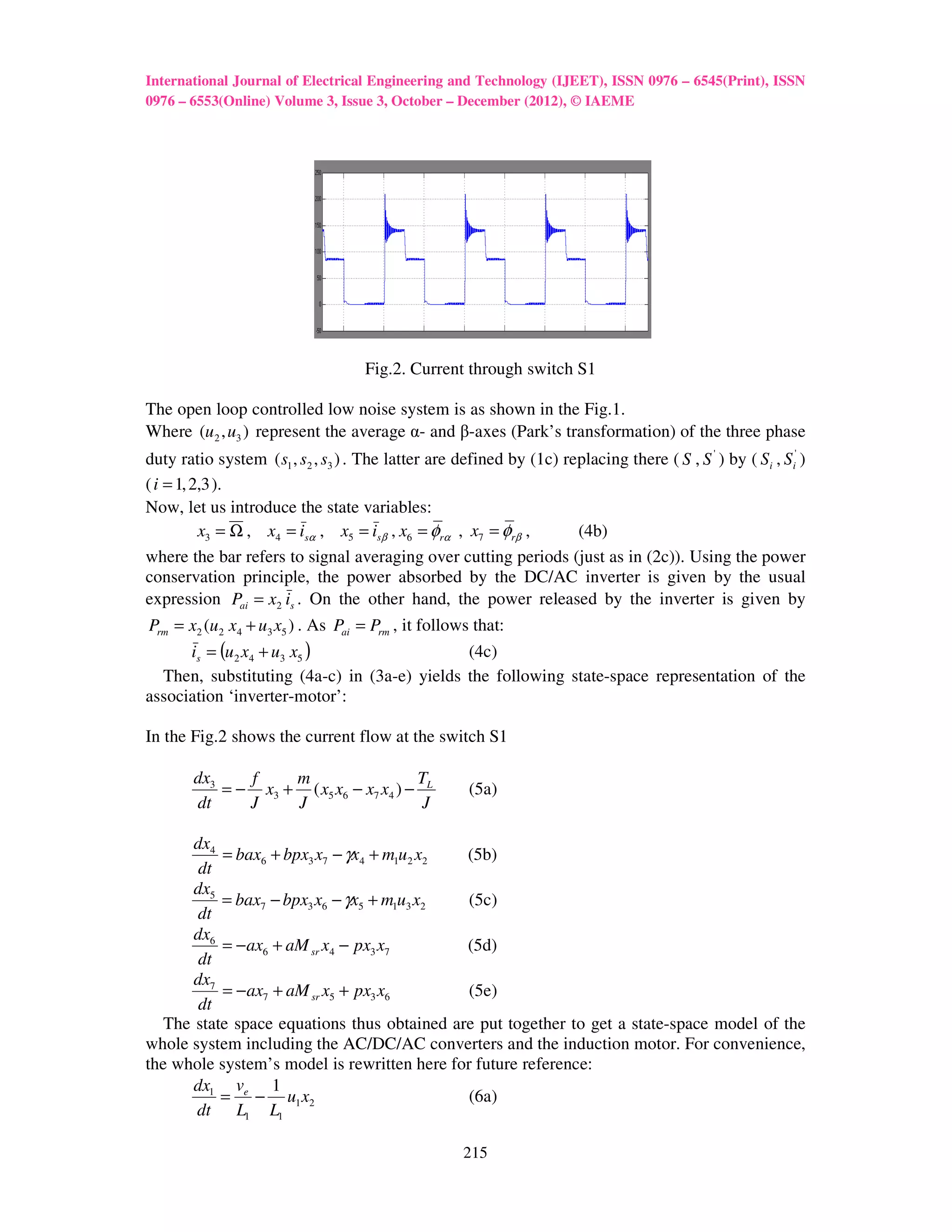
                                    Fig.2. Current through switch S1

The open loop controlled low noise system is as shown in the Fig.1.
Where (u 2 , u3 ) represent the average α- and β-axes (Park’s transformation) of the three phase
duty ratio system ( s1 , s2 , s3 ) . The latter are defined by (1c) replacing there ( S , S ' ) by ( Si , Si' )
( i = 1, 2,3 ).
Now, let us introduce the state variables:
          x3 = Ω , x4 = isα , x5 = isβ , x6 = φrα , x7 = φrβ ,        (4b)
where the bar refers to signal averaging over cutting periods (just as in (2c)). Using the power
conservation principle, the power absorbed by the DC/AC inverter is given by the usual
expression Pai = x2 is . On the other hand, the power released by the inverter is given by
Prm = x2 (u2 x4 + u3 x5 ) . As Pai = Prm , it follows that:
      is = (u 2 x4 + u3 x5 )                         (4c)
  Then, substituting (4a-c) in (3a-e) yields the following state-space representation of the
association ‘inverter-motor’:

In the Fig.2 shows the current flow at the switch S1

        dx3    f    m                   T
            = − x3 + ( x5 x6 − x7 x4 ) − L            (5a)
        dt     J    J                    J

       dx4
           = bax6 + bpx3 x7 − γx4 + m1u2 x2  (5b)
        dt
       dx5
           = bax7 − bpx3 x6 − γx5 + m1u3 x2   (5c)
       dt
       dx6
           = − ax6 + aM sr x4 − px3 x7       (5d)
        dt
       dx7
           = − ax7 + aM sr x5 + px3 x6        (5e)
        dt
   The state space equations thus obtained are put together to get a state-space model of the
whole system including the AC/DC/AC converters and the induction motor. For convenience,
the whole system’s model is rewritten here for future reference:
       dx1 ve 1
           = − u1 x2                          (6a)
       dt L1 L1

                                                     215
International Journal of Electrical Engineering and Technology (IJEET), ISSN 0976 – 6545(Print), ISSN
0976 – 6553(Online) Volume 3, Issue 3, October – December (2012), © IAEME

       dx2      1           1
             =     u1 x1 −    (u 2 x4 + u3 x5 )     (6b)
        dt     2C          2C
       dx3       f        m                    T
             = − x3 + ( x5 x6 − x7 x4 ) − L         (6c)
       dt        J        J                     J
       dx4
             = bax6 + bpx3 x7 − γx4 + m1u 2 x2      (6d)
        dt
       dx5
             = bax7 − bpx3 x6 − γx5 + m1u3 x2       (6e)
       dt
       dx6
             = −ax6 + aM sr x4 − px3 x7             (6f)
       dt
       dx7
             = −ax 7 + aM sr x5 + px3 x6            (6g)
        dt


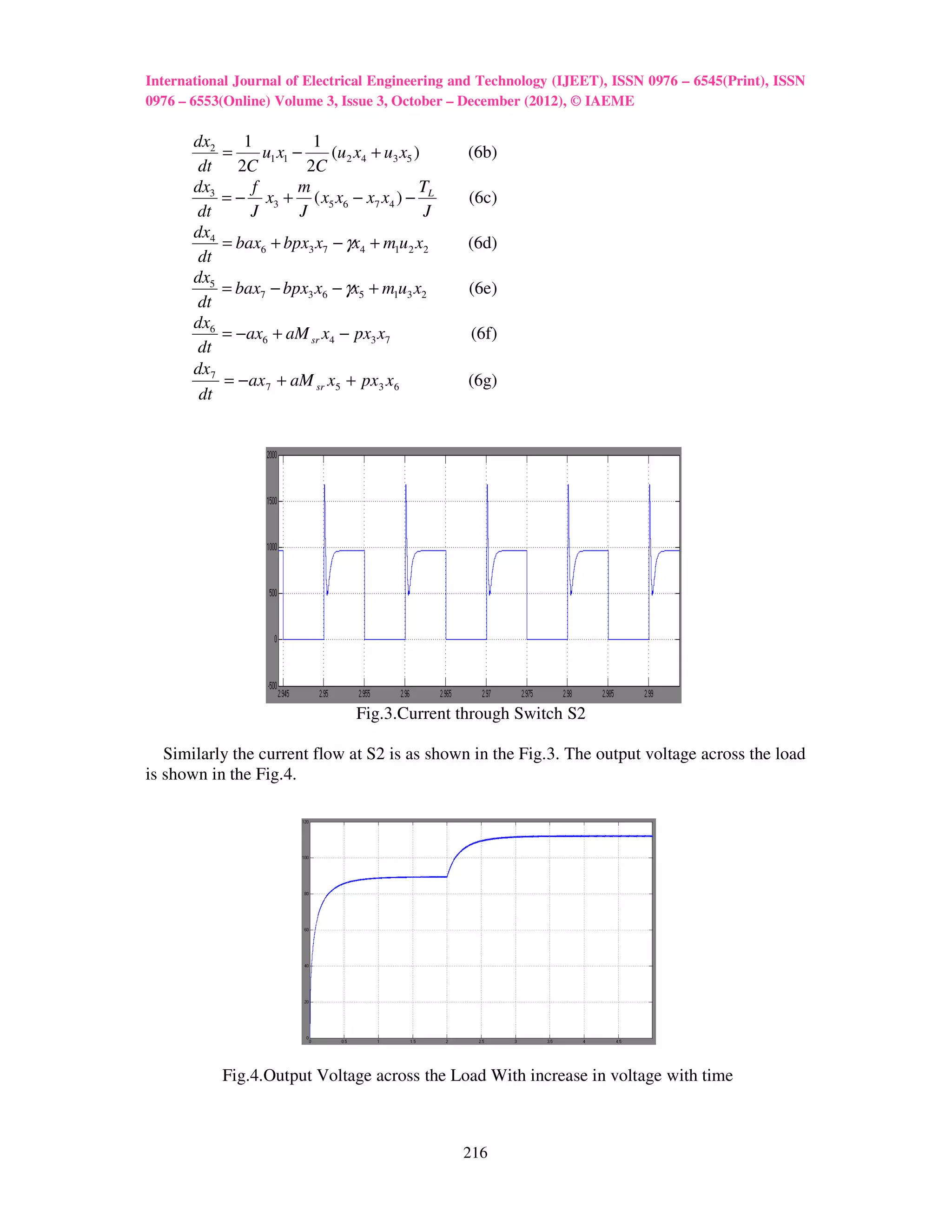
                                   Fig.3.Current through Switch S2

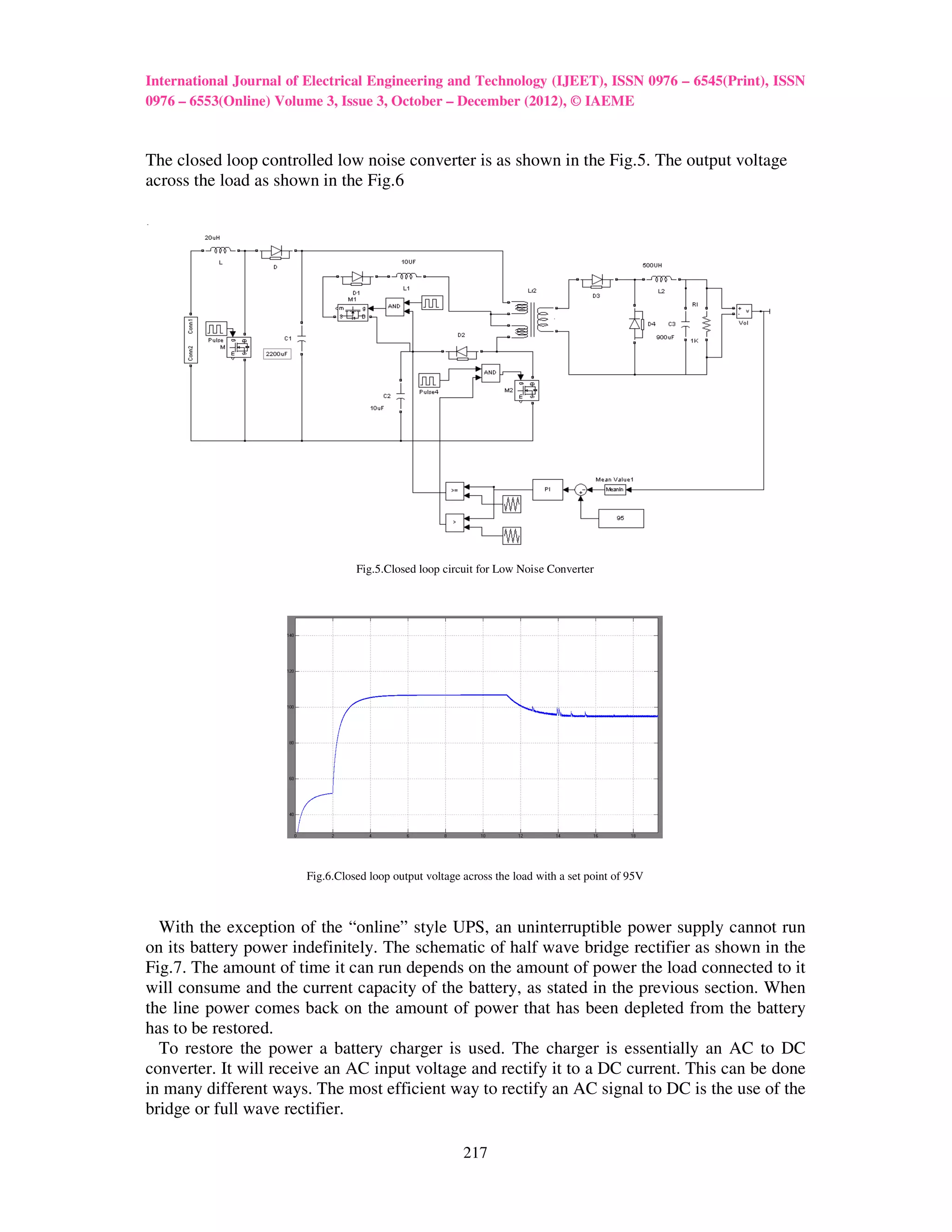
   Similarly the current flow at S2 is as shown in the Fig.3. The output voltage across the load
is shown in the Fig.4.


             Fig.4.Output Voltage across the Load With increase in voltage with time


                                                    216
International Journal of Electrical Engineering and Technology (IJEET), ISSN 0976 – 6545(Print), ISSN
0976 – 6553(Online) Volume 3, Issue 3, October – December (2012), © IAEME


The closed loop controlled low noise converter is as shown in the Fig.5. The output voltage
across the load as shown in the Fig.6

.


                                  Fig.5.Closed loop circuit for Low Noise Converter


                        Fig.6.Closed loop output voltage across the load with a set point of 95V


  With the exception of the “online” style UPS, an uninterruptible power supply cannot run
on its battery power indefinitely. The schematic of half wave bridge rectifier as shown in the
Fig.7. The amount of time it can run depends on the amount of power the load connected to it
will consume and the current capacity of the battery, as stated in the previous section. When
the line power comes back on the amount of power that has been depleted from the battery
has to be restored.
  To restore the power a battery charger is used. The charger is essentially an AC to DC
converter. It will receive an AC input voltage and rectify it to a DC current. This can be done
in many different ways. The most efficient way to rectify an AC signal to DC is the use of the
bridge or full wave rectifier.

                                                         217
International Journal of Electrical Engineering and Technology (IJEET), ISSN 0976 – 6545(Print), ISSN
0976 – 6553(Online) Volume 3, Issue 3, October – December (2012), © IAEME

  When the AC source is outputting it positive current the diode D1 and D2 conduct creating
a positive output across the resistor RL. When the AC source transitions into its negative
current output, diodes D1 and D2 no longer conduct, but diodes D3 and D4 begin to conduct
and then fully turn on. When this happens the current direction through RL stays the same
keeping the output voltage positive. This causes the
output of the circuit to be a purely DC output.


                      Fig. 7. Schematic of a bridge or full wave rectifier

  The inverter section of the UPS is conversion device that will convert a DC signal to an
AC signal. It takes the DC power supplied by the battery and converts it to a usable AC
power for the component.


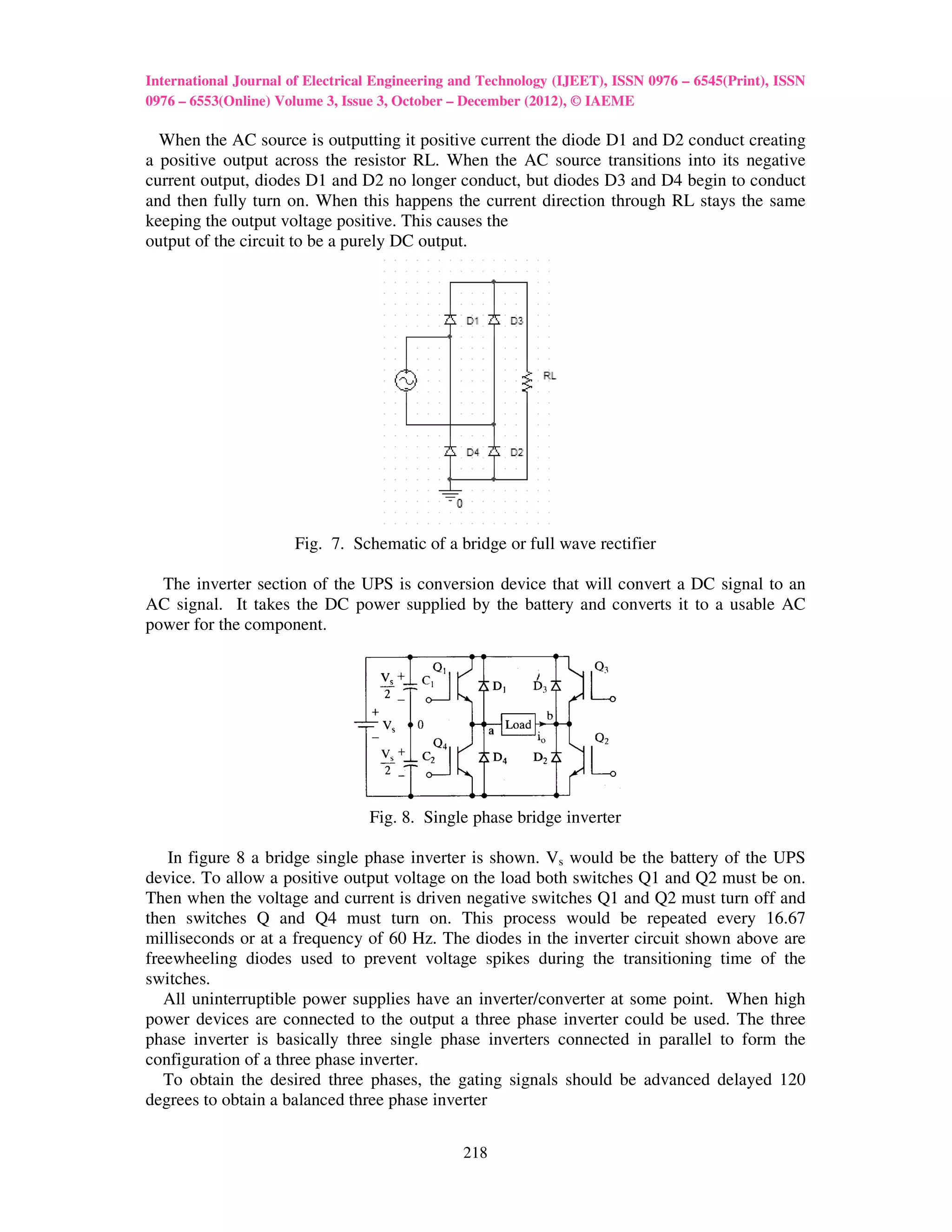
                                  Fig. 8. Single phase bridge inverter

   In figure 8 a bridge single phase inverter is shown. Vs would be the battery of the UPS
device. To allow a positive output voltage on the load both switches Q1 and Q2 must be on.
Then when the voltage and current is driven negative switches Q1 and Q2 must turn off and
then switches Q and Q4 must turn on. This process would be repeated every 16.67
milliseconds or at a frequency of 60 Hz. The diodes in the inverter circuit shown above are
freewheeling diodes used to prevent voltage spikes during the transitioning time of the
switches.
   All uninterruptible power supplies have an inverter/converter at some point. When high
power devices are connected to the output a three phase inverter could be used. The three
phase inverter is basically three single phase inverters connected in parallel to form the
configuration of a three phase inverter.
   To obtain the desired three phases, the gating signals should be advanced delayed 120
degrees to obtain a balanced three phase inverter


                                                218
International Journal of Electrical Engineering and Technology (IJEET), ISSN 0976 – 6545(Print), ISSN
0976 – 6553(Online) Volume 3, Issue 3, October – December (2012), © IAEME


                                 Fig.9.Three phase bridge inverter

        In the Fig. 9. Three phase bridge inverter schematic connected in parallel, there will
be six transistors and six diodes. Only two transistor switches will be on at any one time.
        There are six modes of operations in a cycle and each mode is 60 degrees. This allows
there to be three separate phase outputs. When switches Q1 and Q6 are on there is a positive
voltage developed across nodes a and b. To transition from a positive to negative voltage
across node a and b Q1 and Q6 must turn off and then Q4 and Q3 would turn on.
        To complete the remaining two sets of phase voltages across nodes b and c as well as
nodes a and c we will turn on the following switches. Switches Q3 and Q2 will be on for a
positive voltage across node b and c, then switches Q6 and Q5 for a negative voltage across
node b and c. Finally, to obtain a positive voltage across nodes a and c switches Q1 and Q2
will be on, and to develop a negative voltage across these same two nodes switches Q4 and
Q5 need to be on.

IV. CONCLUSION

       This Application Note has demonstrated that the PIC16C620A can be used to perform
simple SMPS controller functions, such as Constant Voltage, Constant Current, or Constant
Voltage with current limit. The program example can be used with any of the PICmicro
family members, which has on-board comparators. These types of units have been configured
to accept different standards in both input voltage and frequency and are also available in
many output power ranges from 560VA to 6KVA.

REFERENCES

[1] Tamer T.N.Khabib, Azah Mohamed, Nowshad Admin,”A New Controller Scheme for
Photo voltaics power generation system,”European journal of scientific research ISSN 1450-
216X vol.33 No.3 (2009), pp.515-524

[2] J.Morroni, R.Zane, D.Maksimovic, ”Design and Implementation of an adaptive tuning
system based on desired phase margin for digitally controlled DC-DC Converters, ”IEEE
Trans. Power Electron.,vol.24,no.2,pp.559-564,feb.2009

[3] M.Shirazi,J.Morroni,A.Dolgov,R.Zane,D.Maksimovic,”Integration of frequency response
measurement capabilities in digital controllers for DC-DC Converters,”IEEETrans.Power
Electron.,vol.23, no.5,pp.2524-2535,sep.2008

[4] Hugo Ribeiro, Beatriz V.Borges,”New single stage, single phase, full Bridge Converter,
“submitted for appreciation to the Technical committee of IEEE ECCE-Energy conversion
congress and exhibition, January 2009

                                                219
International Journal of Electrical Engineering and Technology (IJEET), ISSN 0976 – 6545(Print), ISSN
0976 – 6553(Online) Volume 3, Issue 3, October – December (2012), © IAEME

[5] Y.Yin, M.Shirazi, R.Zane,”Electronic Ballast control IC with digital phase control and
lamp current regulation,”IEEETrans.Power Electron., vol.23, no.1, pp.11-18, jan.2008

[6] Yungtaek Jang,David L.Dillman and Milan M.Javanovie,”A New soft-switched PFC
Boost Rectifier with Integrated Flyback Converter for stand –by Power,”IEEE Trans.on
Power Electronics,pp.66- 72,No.1,2006

[7] Gerry Moschopoulos and Geza Joos, “A Novel Soft-Switched PWM Current Source
Rectifier/ Inverter”, Proc. of 25th IEEE Annual Power Electronics Specialists Conference,
pp.978-984, 2010

[8] R.W. De Doncker “The Auxiliary Resonant Commutated                Pole Converter”, IEEE IAS
’10 Records, pp.829-834, 2010

[9] W.MacMarray “Resonant Snubbers with Auxiliary Switches”, IEEEIAS7 ’11 Records,
pp.829-834, 2011

[10] Braz J. Cardoso Filho, Steffen Bernet and Thomas A. Lipo, “A New Control Strategy for
the PWM Current Stiff Rectifier/Inverter with Resonant Snubber”, Proc. of 28th IEEE
Annual Power Electronics Specialists Conference, pp.574-579, June, 2011

[11] S. Abe, T. Ninomiya, Comparison of Active-Clamp and ZVT Techniques Applied to
Tapped-Inductor DC-DC Converter with Low Voltage and High Current, Journal of Power
Electronics, Vol.2, No.3, pp.199-205, 2011

[12] Arturo Fernandez,Member,IEEE,Javier sebastin,Member IEEE,Maria Hernando
Member IEEE,”Multiple output AC/DC Converter with an Internal DC UPS,”IEEE Trans on
Industrial Electronics.vol.53.no.1.Feb.2011

BIOGRAPHY

                  Dr.S.Sankar obtained his B.E Degree in Electrical & Electronics
                  Engineering at Sri Venkateswara College of Engineering, from Madras
                  University and M.E (Power System) Degree from Annamalai University
                  Chidambaram. He has done his Ph.D in the area of FACTS controllers in
                  2011. His research interests are in the area of FACTS, Electrical Machines,
                  Voltage stability, power quality, Power system security and Power System
                  Analysis.


                     Dr S.SARAVANAKUMAR has more than 10 years of teaching and
                  research experience. He did his Postgraduate in ME in Computer Science
                  and Engineering at Bharath engineering college,anna university chennai, and
                  Ph.D in Computer Science and Engineering at Bharath University, Chennai.
                  He has guiding a number of research scholars in the area Adhoc Network,
                  ANN, Security in Sensor Networks, Mobile Database and Data Mining
                  under Bharath University Chennai, Sathayabama University and Bharathiyar
                  University.

                                                220
International Journal of Electrical Engineering and Technology (IJEET), ISSN 0976 – 6545(Print), ISSN
0976 – 6553(Online) Volume 3, Issue 3, October – December (2012), © IAEME


                 Mr.M.PADMARASAN has completed his B.E. in Priyadharshini
                 Engineering College, Vaniyambadi. He completed his M.E. (Power System
                 Engineering) at Annamalai University, Chidambaram in the year of 2004. He
                 is a Research Scholar in Sathyabama University. His area of interest is
                 Power System Stability, Dynamics, Renewable Power Generation, Hybrid
                 Power Generation & High Voltage Engineering. He published various papers
                 in International Journals & Conferences.

                  Mr.C.T.MANIKANDAN has completed his B.E. in V.R.S College of
                 Engineering and Technology,Arasur. He completed his M.E. (Power
                 Electronics and Drives) at Anna University, Chennai in the year of 2009. His
                 area of interest is DC-DC converters,Inverters ,Electrical Machines,Power
                 Qualityand Facts devices. He published various papers in International
                 Journals & Conferences.Conferences.


                 D.Jayalakshmi obtained her B.E Degree in Electrical & Electronics
                 Engineering at Jaya College of Engineering, from Madras University and
                 M.E (Power System) Degree from AnnaUniversity Chennai.. Her area of
                 interest is Power System Stability, Dynamics, Renewable Power Generation,
                 Hybrid Power Generation & High Voltage Engineering. She published
                 various papers in International Journals & Conferences.


                                                221

Analysis of low noise smps system

  • 1.
    INTERNATIONAL Issue 3,October – December (2012), © IAEME 0976 – 6545(Print), ISSN International Journal of Electrical Engineering and Technology (IJEET), ISSN 0976 – 6553(Online) Volume 3, JOURNAL OF ELECTRICAL ENGINEERING & TECHNOLOGY (IJEET) ISSN 0976 – 6545(Print) ISSN 0976 – 6553(Online) Volume 3, Issue 3, October - December (2012), pp. 211-221 IJEET © IAEME: www.iaeme.com/ijeet.asp Journal Impact Factor (2012): 3.2031 (Calculated by GISI) ©IAEME www.jifactor.com ANALYSIS OF LOW NOISE SMPS SYSTEM 1 S.Sankar, 2S.Saravanakumar, 3M.Padmarasan, 4C.T .Manikandan, 5D.Jayalakshmi 1 Professor of EEE, Panimalar Institute of Technology, Chennai, TamilNadu, India,ssankarphd@yahoo.com 2 Professor of IT, Panimalar Institute of Technology, Chennai, Tamilnadu, India,saravanakumars81@gmail.com 3 Assistant Professor of of EEE, Panimalar Institute ofTechnology, Chennai, Tamilnadu, India,padmaras_mathi@yahoo.com 4 Assistant Professor of of EEE, Panimalar Institute ofTechnology, Chennai, Tamilnadu, India,manikandanct@yahoo.com 5 Assistant Professor of of EEE, Research scholar, St.Peters University, Chennai, TamilNadu, India, djayalakshmi28@gmail.com ABSTRACT The analysis of open and closed loop controlled DC-DC converter in SMPS system is analyzed in this paper. A new model of soft switching DC-DC converter topology with circuit is presented in this paper for the switching mode power supply applications. It is a type of power converter. Such electronic devices often contain several sub-circuits, each with its own voltage level require different from that supplied by the battery or an external. Additionally, the battery voltage declines as its stored power is drained. SMPS DC to DC converters offer a method to increase voltage from a partially lowered battery voltage thereby saving space instead of using multiple batteries to accomplish the same thing and the UPS operation at different modes are analyzed. Index Terms: DC-DC converter, Zero voltage soft switching, Zero current soft switching, Converter, Inverter. 1. INTRODUCTION A switched-mode power supply (switching-mode power supply, SMPS, or switcher) is an electronic power supply that incorporates a switching regulator to convert electrical power efficiently. Like other power supplies, an SMPS transfers power from a source, like mains power, to a load, such as a personal computer, while converting voltage and current characteristics. An SMPS is usually employed to efficiently provide a regulated output 211
  • 2.
    International Journal ofElectrical Engineering and Technology (IJEET), ISSN 0976 – 6545(Print), ISSN 0976 – 6553(Online) Volume 3, Issue 3, October – December (2012), © IAEME voltage, typically at a level different from the input voltage. Unlike a linear power supply, the pass transistor of a switching-mode supply continually switches between low-dissipation, full-on and full-off states, and spends very little time in the high dissipation transitions (which minimizes wasted energy). Ideally, a switched-mode power supply dissipates no power. Voltage regulation is achieved by varying the ratio of on-to-off time. In contrast, a linear power supply regulates the output voltage by continually dissipating power in the pass transistor. This higher power conversion efficiency is an important advantage of a switched- mode power supply. Switched-mode power supplies may also be substantially smaller and lighter than a linear supply due to the smaller transformer size and weight. Switching regulators are used as replacements for the linear regulators when higher efficiency, smaller size or lighter weights are required. They are, however, more complicated; their switching currents can cause electrical noise problems if not carefully suppressed, and simple designs may have a poor factor. The switching power semiconductor in the SMPS system, the problem of the switching loss and EMI/RFI noises has been closed up. This course produced the EMC limitation like the International Special Committee on Radio Interference (CISPR) and the harmonics limitation like the International Electro technical Commission (IEC). For keeping up with the limitation, the SMPS system must add its system to the noise filter and the metal and magnetic component shield for the EMI/RFI noises and to the PFC converter circuit and the large input filter for the input harmonic current. On the other hand, the power semiconductor device technology development can achieve the high frequency switching operation in the SMPS system. The increases of the switching losses have been occurred by this high frequency switching operation. Of course, the inductor and transformer size have been reduced by the high frequency switching, while the size of cooling fan could be huge because of the increase of the switching losses. By using LC resonant phenomenon, this technique can minimize the switching power losses of the power semiconductor devices, and reduce their electrical dynamic and peak stresses, voltage and current surge-related EMI/RFI noises under high frequency switching strategy. Thus, a new conceptual circuit configuration of the advanced forward type soft switching DC-DC converter which has the neutral point inductor connected auxiliary resonant snubber (NPC-ARS) circuit is presented in this paper with its operating principle in steady state. In addition, its fundamental operation and its performance characteristics of the proposed forward type soft switching DC-DC converter treated here are evaluated on the basis of experimental results. A New Controller scheme for Photo voltaics power generation system is presented in [1]. The design and implementation of an adaptive tuning system based on desired phase margin for digitally controlled DC to DC Converters is given in [2]. Integration of frequency response measurement capabilities in digital controllers for DC to DC Converters is given in [3]. A New single stage, single phase, full bridge converter is presented in [4]. The Electronic ballast control IC with digital phase control and lamp current regulation is given in [5]. A New soft-switched PFC Boost rectifier/inverter is presented in [6]. Novel soft switched PWM current source rectifier is presented in [7]. The auxiliary resonant commutated pole converter is given by [8].Resonant snubbers with auxiliary switches are given in [9]. A control strategy for PWM current source rectifier is given in [10].Comparison of active clamp ZVT techniques applied to tapped inductor DC-DC converter is given in [11].The multiple output AC/DC Converter with an internal DC UPS is given in [12].The Bi-directional isolated DC-DC Converter for next generation power distribution – comparison of converters using Si and Sic devices are presented. The above literature does not deal with modeling and simulation of closed loop controlled SMPS System employing forward converter. This work aims to develop a model for the Closed loop SMPS System. 212
  • 3.
    International Journal ofElectrical Engineering and Technology (IJEET), ISSN 0976 – 6545(Print), ISSN 0976 – 6553(Online) Volume 3, Issue 3, October – December (2012), © IAEME In some cases, the output ripple of the converter may still be higher than desired, even with the proper inductor and capacitor selections. In this case, an additional inductor and capacitor may be used as a low pass filter at the converter output. A DC/DC Converter is normally chosen because of its high efficiency in converting the input power to output power. Unlike a linear regulator, the efficiency measure of a DC/DC Converter generally increases as its load increases. A properly designed DC/DC Converter can yield an efficiency measure of greater than 90% at full load. The efficiency of a DC/DC Converter is expressed as the ratio of output power and input power. The following equations can be used to determine efficiency. II. Analysis of DC converter system The power supply network is connected to an H-bridge converter consisting of four IGBT’s with anti-parallel diodes for bidirectional power flow mode. The converter should be controlled so that two main tasks are accomplished: (i) providing a constant DC link voltage; (ii) ensuring an almost unitary power factor connection with the power network. Applying Kirchhoff’s laws, this subsystem is described by the following set of differential equations: die ve 1 = − s vdc (1a) dt L1 L1 dvdc 1 1 = s ie − is (1b) dt 2C 2C where ie is the current in inductor L1 , vdc denotes the voltage in capacitor 2C , is designates the input current inverter, ve = 2 .E. cos(ωet ) is the sinusoidal network voltage (with known constants E , ωe ) and s is the switch position function taking values in the discrete set { − 1, 1 }. Specifically:  1 if S is ON and S ′ is OFF (1c) s= − 1 if S is OFF and S ′ is ON The above (instantaneous) model describes accurately the physical inverter. Then, it is based upon to build up converter simulators. However, it is not suitable for control design due to the switched nature of the control input s . As a matter of fact, most existing nonlinear control approaches apply to systems with continuous control inputs. Therefore, the control design for the above converter will be performed using the following average version of (1a-b) [6]: dx1 ve 1 = − u1 x2 (2a) dt L1 L1 dx2 1 1 = u1 x1 − is (2b) dt 2C 2C where: x1 = ie , x2 = vdc , u1 = s (2c) are the average values over the cutting periods of ie , vdc and s , respectively. 213
  • 4.
    International Journal ofElectrical Engineering and Technology (IJEET), ISSN 0976 – 6545(Print), ISSN 0976 – 6553(Online) Volume 3, Issue 3, October – December (2012), © IAEME III. Modeling of Inverter system The inverter model is based on the motor equations in the rotating α -and- β axes and reads as: dΩ f m T = − Ω + (isβ φrα − isα φrβ ) − L (3a) dt J J J disα = baφrα + bpΩφrβ − γisα + m1vsα (3b) dt disβ = baφrβ − bpΩφrα − γisβ + m1vsβ (3c) dt dφ r α = −aφrα + aM sr isα − pΩφrβ (3d) dt dφ r β = −aφrβ + aM sr isβ + pΩφrα (3e) dt where isα , isβ , φrα , φrβ , Ω , and, TL , are the stator currents, rotor fluxes, angular speed, and load torque, respectively. Wherever they come in, the subscripts s and r refer to the stator and rotor, respectively. That is, Rs and Rr are the stator and rotor resistances; Ls and Lr are the self-inductances. M sr denotes the mutual inductance between the stator and rotor windings. p designates the number of pole-pairs, J the inertia of the motor-load set, and f is the friction coefficient. The remaining parameters are defined as follows: R M sr 2 2 2 2 M a = r ,b = , γ = ( Lr Rs + M sr Rr ) / σLs Lr , σ = 1 − ( M sr / Ls Lr ) , m = p sr , Lr σLs Lr Lr 1 m1 = . σLs In (3a-e), vsα , vsβ are the stator voltage in the αβ -coordinates (Park’s transformation of the three phase stator voltages). The inverter is featured by the fact that the stator α- and β- voltages can be controlled independently. To this end, these voltages are expressed in function of the corresponding control action (see e.g. [2]): vsβ = vdc u3 , vsα = vdc u 2 (4a) Fig.1.Open loop circuit for Low Noise Converter 214
  • 5.
    International Journal ofElectrical Engineering and Technology (IJEET), ISSN 0976 – 6545(Print), ISSN 0976 – 6553(Online) Volume 3, Issue 3, October – December (2012), © IAEME Fig.2. Current through switch S1 The open loop controlled low noise system is as shown in the Fig.1. Where (u 2 , u3 ) represent the average α- and β-axes (Park’s transformation) of the three phase duty ratio system ( s1 , s2 , s3 ) . The latter are defined by (1c) replacing there ( S , S ' ) by ( Si , Si' ) ( i = 1, 2,3 ). Now, let us introduce the state variables: x3 = Ω , x4 = isα , x5 = isβ , x6 = φrα , x7 = φrβ , (4b) where the bar refers to signal averaging over cutting periods (just as in (2c)). Using the power conservation principle, the power absorbed by the DC/AC inverter is given by the usual expression Pai = x2 is . On the other hand, the power released by the inverter is given by Prm = x2 (u2 x4 + u3 x5 ) . As Pai = Prm , it follows that: is = (u 2 x4 + u3 x5 ) (4c) Then, substituting (4a-c) in (3a-e) yields the following state-space representation of the association ‘inverter-motor’: In the Fig.2 shows the current flow at the switch S1 dx3 f m T = − x3 + ( x5 x6 − x7 x4 ) − L (5a) dt J J J dx4 = bax6 + bpx3 x7 − γx4 + m1u2 x2 (5b) dt dx5 = bax7 − bpx3 x6 − γx5 + m1u3 x2 (5c) dt dx6 = − ax6 + aM sr x4 − px3 x7 (5d) dt dx7 = − ax7 + aM sr x5 + px3 x6 (5e) dt The state space equations thus obtained are put together to get a state-space model of the whole system including the AC/DC/AC converters and the induction motor. For convenience, the whole system’s model is rewritten here for future reference: dx1 ve 1 = − u1 x2 (6a) dt L1 L1 215
  • 6.
    International Journal ofElectrical Engineering and Technology (IJEET), ISSN 0976 – 6545(Print), ISSN 0976 – 6553(Online) Volume 3, Issue 3, October – December (2012), © IAEME dx2 1 1 = u1 x1 − (u 2 x4 + u3 x5 ) (6b) dt 2C 2C dx3 f m T = − x3 + ( x5 x6 − x7 x4 ) − L (6c) dt J J J dx4 = bax6 + bpx3 x7 − γx4 + m1u 2 x2 (6d) dt dx5 = bax7 − bpx3 x6 − γx5 + m1u3 x2 (6e) dt dx6 = −ax6 + aM sr x4 − px3 x7 (6f) dt dx7 = −ax 7 + aM sr x5 + px3 x6 (6g) dt Fig.3.Current through Switch S2 Similarly the current flow at S2 is as shown in the Fig.3. The output voltage across the load is shown in the Fig.4. Fig.4.Output Voltage across the Load With increase in voltage with time 216
  • 7.
    International Journal ofElectrical Engineering and Technology (IJEET), ISSN 0976 – 6545(Print), ISSN 0976 – 6553(Online) Volume 3, Issue 3, October – December (2012), © IAEME The closed loop controlled low noise converter is as shown in the Fig.5. The output voltage across the load as shown in the Fig.6 . Fig.5.Closed loop circuit for Low Noise Converter Fig.6.Closed loop output voltage across the load with a set point of 95V With the exception of the “online” style UPS, an uninterruptible power supply cannot run on its battery power indefinitely. The schematic of half wave bridge rectifier as shown in the Fig.7. The amount of time it can run depends on the amount of power the load connected to it will consume and the current capacity of the battery, as stated in the previous section. When the line power comes back on the amount of power that has been depleted from the battery has to be restored. To restore the power a battery charger is used. The charger is essentially an AC to DC converter. It will receive an AC input voltage and rectify it to a DC current. This can be done in many different ways. The most efficient way to rectify an AC signal to DC is the use of the bridge or full wave rectifier. 217
  • 8.
    International Journal ofElectrical Engineering and Technology (IJEET), ISSN 0976 – 6545(Print), ISSN 0976 – 6553(Online) Volume 3, Issue 3, October – December (2012), © IAEME When the AC source is outputting it positive current the diode D1 and D2 conduct creating a positive output across the resistor RL. When the AC source transitions into its negative current output, diodes D1 and D2 no longer conduct, but diodes D3 and D4 begin to conduct and then fully turn on. When this happens the current direction through RL stays the same keeping the output voltage positive. This causes the output of the circuit to be a purely DC output. Fig. 7. Schematic of a bridge or full wave rectifier The inverter section of the UPS is conversion device that will convert a DC signal to an AC signal. It takes the DC power supplied by the battery and converts it to a usable AC power for the component. Fig. 8. Single phase bridge inverter In figure 8 a bridge single phase inverter is shown. Vs would be the battery of the UPS device. To allow a positive output voltage on the load both switches Q1 and Q2 must be on. Then when the voltage and current is driven negative switches Q1 and Q2 must turn off and then switches Q and Q4 must turn on. This process would be repeated every 16.67 milliseconds or at a frequency of 60 Hz. The diodes in the inverter circuit shown above are freewheeling diodes used to prevent voltage spikes during the transitioning time of the switches. All uninterruptible power supplies have an inverter/converter at some point. When high power devices are connected to the output a three phase inverter could be used. The three phase inverter is basically three single phase inverters connected in parallel to form the configuration of a three phase inverter. To obtain the desired three phases, the gating signals should be advanced delayed 120 degrees to obtain a balanced three phase inverter 218
  • 9.
    International Journal ofElectrical Engineering and Technology (IJEET), ISSN 0976 – 6545(Print), ISSN 0976 – 6553(Online) Volume 3, Issue 3, October – December (2012), © IAEME Fig.9.Three phase bridge inverter In the Fig. 9. Three phase bridge inverter schematic connected in parallel, there will be six transistors and six diodes. Only two transistor switches will be on at any one time. There are six modes of operations in a cycle and each mode is 60 degrees. This allows there to be three separate phase outputs. When switches Q1 and Q6 are on there is a positive voltage developed across nodes a and b. To transition from a positive to negative voltage across node a and b Q1 and Q6 must turn off and then Q4 and Q3 would turn on. To complete the remaining two sets of phase voltages across nodes b and c as well as nodes a and c we will turn on the following switches. Switches Q3 and Q2 will be on for a positive voltage across node b and c, then switches Q6 and Q5 for a negative voltage across node b and c. Finally, to obtain a positive voltage across nodes a and c switches Q1 and Q2 will be on, and to develop a negative voltage across these same two nodes switches Q4 and Q5 need to be on. IV. CONCLUSION This Application Note has demonstrated that the PIC16C620A can be used to perform simple SMPS controller functions, such as Constant Voltage, Constant Current, or Constant Voltage with current limit. The program example can be used with any of the PICmicro family members, which has on-board comparators. These types of units have been configured to accept different standards in both input voltage and frequency and are also available in many output power ranges from 560VA to 6KVA. REFERENCES [1] Tamer T.N.Khabib, Azah Mohamed, Nowshad Admin,”A New Controller Scheme for Photo voltaics power generation system,”European journal of scientific research ISSN 1450- 216X vol.33 No.3 (2009), pp.515-524 [2] J.Morroni, R.Zane, D.Maksimovic, ”Design and Implementation of an adaptive tuning system based on desired phase margin for digitally controlled DC-DC Converters, ”IEEE Trans. Power Electron.,vol.24,no.2,pp.559-564,feb.2009 [3] M.Shirazi,J.Morroni,A.Dolgov,R.Zane,D.Maksimovic,”Integration of frequency response measurement capabilities in digital controllers for DC-DC Converters,”IEEETrans.Power Electron.,vol.23, no.5,pp.2524-2535,sep.2008 [4] Hugo Ribeiro, Beatriz V.Borges,”New single stage, single phase, full Bridge Converter, “submitted for appreciation to the Technical committee of IEEE ECCE-Energy conversion congress and exhibition, January 2009 219
  • 10.
    International Journal ofElectrical Engineering and Technology (IJEET), ISSN 0976 – 6545(Print), ISSN 0976 – 6553(Online) Volume 3, Issue 3, October – December (2012), © IAEME [5] Y.Yin, M.Shirazi, R.Zane,”Electronic Ballast control IC with digital phase control and lamp current regulation,”IEEETrans.Power Electron., vol.23, no.1, pp.11-18, jan.2008 [6] Yungtaek Jang,David L.Dillman and Milan M.Javanovie,”A New soft-switched PFC Boost Rectifier with Integrated Flyback Converter for stand –by Power,”IEEE Trans.on Power Electronics,pp.66- 72,No.1,2006 [7] Gerry Moschopoulos and Geza Joos, “A Novel Soft-Switched PWM Current Source Rectifier/ Inverter”, Proc. of 25th IEEE Annual Power Electronics Specialists Conference, pp.978-984, 2010 [8] R.W. De Doncker “The Auxiliary Resonant Commutated Pole Converter”, IEEE IAS ’10 Records, pp.829-834, 2010 [9] W.MacMarray “Resonant Snubbers with Auxiliary Switches”, IEEEIAS7 ’11 Records, pp.829-834, 2011 [10] Braz J. Cardoso Filho, Steffen Bernet and Thomas A. Lipo, “A New Control Strategy for the PWM Current Stiff Rectifier/Inverter with Resonant Snubber”, Proc. of 28th IEEE Annual Power Electronics Specialists Conference, pp.574-579, June, 2011 [11] S. Abe, T. Ninomiya, Comparison of Active-Clamp and ZVT Techniques Applied to Tapped-Inductor DC-DC Converter with Low Voltage and High Current, Journal of Power Electronics, Vol.2, No.3, pp.199-205, 2011 [12] Arturo Fernandez,Member,IEEE,Javier sebastin,Member IEEE,Maria Hernando Member IEEE,”Multiple output AC/DC Converter with an Internal DC UPS,”IEEE Trans on Industrial Electronics.vol.53.no.1.Feb.2011 BIOGRAPHY Dr.S.Sankar obtained his B.E Degree in Electrical & Electronics Engineering at Sri Venkateswara College of Engineering, from Madras University and M.E (Power System) Degree from Annamalai University Chidambaram. He has done his Ph.D in the area of FACTS controllers in 2011. His research interests are in the area of FACTS, Electrical Machines, Voltage stability, power quality, Power system security and Power System Analysis. Dr S.SARAVANAKUMAR has more than 10 years of teaching and research experience. He did his Postgraduate in ME in Computer Science and Engineering at Bharath engineering college,anna university chennai, and Ph.D in Computer Science and Engineering at Bharath University, Chennai. He has guiding a number of research scholars in the area Adhoc Network, ANN, Security in Sensor Networks, Mobile Database and Data Mining under Bharath University Chennai, Sathayabama University and Bharathiyar University. 220
  • 11.
    International Journal ofElectrical Engineering and Technology (IJEET), ISSN 0976 – 6545(Print), ISSN 0976 – 6553(Online) Volume 3, Issue 3, October – December (2012), © IAEME Mr.M.PADMARASAN has completed his B.E. in Priyadharshini Engineering College, Vaniyambadi. He completed his M.E. (Power System Engineering) at Annamalai University, Chidambaram in the year of 2004. He is a Research Scholar in Sathyabama University. His area of interest is Power System Stability, Dynamics, Renewable Power Generation, Hybrid Power Generation & High Voltage Engineering. He published various papers in International Journals & Conferences. Mr.C.T.MANIKANDAN has completed his B.E. in V.R.S College of Engineering and Technology,Arasur. He completed his M.E. (Power Electronics and Drives) at Anna University, Chennai in the year of 2009. His area of interest is DC-DC converters,Inverters ,Electrical Machines,Power Qualityand Facts devices. He published various papers in International Journals & Conferences.Conferences. D.Jayalakshmi obtained her B.E Degree in Electrical & Electronics Engineering at Jaya College of Engineering, from Madras University and M.E (Power System) Degree from AnnaUniversity Chennai.. Her area of interest is Power System Stability, Dynamics, Renewable Power Generation, Hybrid Power Generation & High Voltage Engineering. She published various papers in International Journals & Conferences. 221