IC fabrication and OP amp 2 marks.pdf
•
0 likes•24 views

Integrated circuits (ICs) have several advantages over discrete components including reduced cost due to batch processing, increased component density due to miniaturization, and increased reliability. The basic processes for fabricating ICs using planar technology include preparing silicon wafers, depositing dielectric layers, doping, lithography, etching, and metallization. Operational amplifiers have ideal characteristics including infinite input impedance and gain but practical op-amps have limitations such as finite but high input impedance and gain. Negative feedback is used to stabilize the gain of op-amps.

Recommended
More Related Content
Similar to IC fabrication and OP amp 2 marks.pdf
Similar to IC fabrication and OP amp 2 marks.pdf (20)
More from AdhithyaS5
More from AdhithyaS5 (20)
Recently uploaded
Recently uploaded (20)
IC fabrication and OP amp 2 marks.pdf
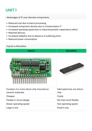
- 1. UNIT 1 Advantages of IC over discrete components. Reduced cost due to batch processing. Increased component density due to miniaturization. P Increased operating speed due to reduced parasitic capacitance effect. Matched devices. Increased reliability due to absence of soldering joints. Reduced power consumption. Hybrid vs Monolithic Hybrid Monolithic Contains 2 or more silicon chip mounted on ceramic substrate. Fabricated only one silicon chip Cheaper Costly Flexible in circuit design Not that much flexible Slower operating speed Fast operating speed Large in size Small in size
- 2. Classification of IC What are the basic processes involved in fabricating ICs using planar technology?
- 3. List out the steps used in the preparation of Si wafers. What is dielectric isolation? A layer of dielectric (usually or ruby) is used to provide electrical and physical isolation from other components of IC. With this isolation there is negligible parasitic capacitance. Expensive to manufacture. What are the two important properties of ? Excellent insulator. Very stable. It is can easily deposited and grown thermally on silicon wafers. SiO2 SiO2
- 4. What are the different types of lithography? Types of lithography Electron beam lithography. X-ray lithography. What is optical lithography? Etching (removing) IC with light is called photo lithography or optical lithography. Distinguish between dry etching and wet etching. Dry etching Wet etching Chemical reagents are used in gaseous form . Chemical reagents used are in liquid form. More accurate and small size can be achieved Less accurate Expensive because specialized equipment is needed. Cheap because only chemical bath is needed. What are the advantages of ion implantation technique? Done at lower temperature so there is lesser tendency of lateral spreading. Depth and Dose of impurity can can be carefully controlled by changing the voltage. What is metallization? Deposition of metal film on IC to make electrical inter-connection between the components and outside world. Usually Al is used since it is a very good conductor. Makes good mechanical bond with silicon. Easy to deposit using vacuum deposition and it makes good bond with Si. Forms ohmic or non rectifying contact with P-type silicon and heavily doped N- type.
- 5. Define diffusion The process of adding impurity to Si wafer is diffusion. It is carried out in high temperature. Differentiate the ideal and practical characteristics of an op-amp. Ideal Practical Infinite input impedance Very high input impedance Infinite voltage gain Very high voltage gain in the order of or Zero output impedance Very Less output impedance Infinite bandwidth Wide bandwidth Infinite slew rate Very high slew rate Infinite CMRR Very high CMRR Define input bias current of an operational amplifier. It is the average of the 2 DC currents flowing into the input terminals of OP amp. What are the causes of slew rate? It is caused usually by capacitance inside or outside the op-amp. This capacitance is which prevents the output respond to input instantly. Define input offset current of an operational amplifier. It is difference between current flowing into input terminals. Write the saturation level of an IC 741. Mention different available IC package configurations. 10 5 10 8 IB = I + B + I − B 2 IOS = I + B − I − B
- 6. State the types of compensation used in an op-amp. Draw the frequency response of an op-amp. Define input offset voltage. It is voltage that needs to be applied in input terminal to get Zero output voltage. Define CMRR of an op-amp. It is the ability of an Op-amp to reject common mode signal. CM RR = Ad Ac
- 7. Define thermal drift. Change in ==Bias voltage, Bias current , Offset current == with temperature is called thermal drift. How is the gain stabilized by negative feedback? What is an inverting amplifier? A circuit that amplifies with inverting the output is called Non-inverting amplifier. What is a Non inverting amplifier? A circuit that amplifies without inverting the output is called Non-inverting amplifier. How an op-amp can be used as a voltage follower? What is a summer? What is differential amplifier? A circuit which amplifies the difference b/w two signals is called differential amplifier. List the applications of V-I converter? List the applications of I-V converter? Draw the circuit diagram of V-I converter? Draw the circuit diagram of I-V converter? Design an adder circuit using an op-amp to get the output expression as
- 8. Design an adder circuit using an op-amp to get the output expression as Vo=- (0.2V1+3V2+5V3) where V1, V2, V3 are the inputs. Disadvantage of ICs If one component fails entire IC has to replaced. Transformer and inductor are impossible to fabricate. Parameters and components of IC cannot be changed, Hence not flexible. Vo = −(V1 + 0.1V2 + 20V3) where V1, V2, V3 are the inputs.