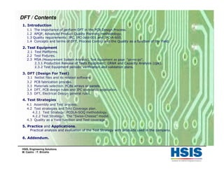
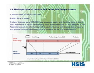
HSIS, Engineering Solutions
M. Castro / F. Briceño
DFT
Design for Test
PCB Design Analysis Focused in Test
and
Advanced Strategic Plan for Tests
Instructors: Mauricio Castro / Francisco Briceño
HSIS – Engineering Solutions
F. Briceño / M. Castro
Jun – 2014
v3.1
DFM / Detalis
Theory and Practice
Using current designs and data from your Company.
Based in IPC Standards, SMTA and the best industry practices.
Conducted by 2 instructors.
Participants: 6 to 9.
Course duration: 4 days (32hrs).
Who can attend:
Design Eng, Tests Eng, Product Eng, Project Eng, NPI Eng,
Manufacturing Eng, Process Eng, Quality Eng, Supplier Quality Eng.
Manufacturing Supervisors, Procurement
Engineering Managers
Requirements to conduct the practices:
LapTop PC.
Gerber Files of 1 or 2 products running or in design process.
Deliverables:
Prints of the course (Manual).
CD, including IPC standards for Design and Acceptability.
HSIS, Engineering Solutions
M. Castro / F. Briceño
DFT / Contents
1. Introduction
1.1 The importance of perform DFT in the PCB Design Process.
1.2 APQP, Advanced Product Quality Planning methodology.
1.3 Quality requirements: IPC, IPC-Jstd-001 and IPC-A-600.
1.4 Concepts and terms of DFT, Process Control and the Quality as a function of the Yield.
2. Test Equipment
2.1 Test Platforms.
2.2 Test Fixtures.
2.3 MSA (Measurement System Analysis), Test Equipment as gage “go-no-go”.
2.3.1 Production Release of Tests Equipment: GR&R and Capacity Analysis (cpk).
2.3.2 Test Equipment periodic verification and validation plans.
3. DFT (Design For Test)
3.1 Netlist files and its related software.
3.2 PCB fabrication process.
3.3 Materials selection. PCBs arrays or panels.
3.4 DFT, PCB design rules and IPC standards application.
3.5 DFT, Electrical Design general rules.
4. Test Strategies
4.1 Assembly and Test process.
4.2 Test strategies and Test Coverage plan.
4.2.1 Test Strategy: PCOLA-SOQ methodology.
4.2.2 Test Strategy: The “Swiss-Cheese” model.
4.3 Quality as a Yield function and Test coverage.
5. Practice and Applications.
Practical analysis and evaluation of the Test Strategy with products used in the company.
6. Addendum.
HSIS, Engineering Solutions
M. Castro / F. Briceño
Introduction
DFT : Design for Tests or Testing or Testability it’s a term derived from DFM.
It’s the process to assure that a Product complies the functional characteristics specified in
the original design. Assuring the most test coverage, giving a product with a minimum or
tending to zero defects.
Application areas:
• DFM - Design For Manufacturability o Manufacturing (includes PCB fabrication DFF and SMT, PTH and
Box Build manufacturing).
• DFT - Design For Testability or Test.
• DFA – Design For Assembly (used for Mechanical Assemblies).
• DFS - Design For Service (used to facilitate servicing products).
• DFR - Design For Reliability.
• DFC - Design For Cost.
• DFE – Design For Environment (green technologies).
• DFU - Design For Usability.
It’s also known as DfX, where X means “eXcellence” that uses all application areas.
But it’s best knowing as DFM.
HSIS, Engineering Solutions
M. Castro / F. Briceño
1.1 The importance of perform DFT in the PCB Design Process.
Why we need to use DFT and DFM
Product Time to Market
Products designed using DFT/DFM have a superior quality and therefore these products
don’t waste time in repairs or debugging. Also, a good execution of DFT/DFM gave to the
Assembler enough time to develop all the required tooling, test fixtures, test programs
and manufacturing process instructions to be ready for the first production run.
HSIS, Engineering Solutions
M. Castro / F. Briceño
Nov - 2014
About the trainers
Francisco Briceño
briceno@hsis.com.mx
Phone: (52)(33) 1665-4766, ID: 72*13*42640
More than 20 years of experience in the Electronics Industry.
Degree in Electro-Mechanical Engineering and a Master Degree in Materials Engineering by IPN
(Instituto Politecnico Nacional) in Mexico City.
Dipl. in Soldering in Electronics by MIT (Massachusetts Institute Technological).
Certified as Black Belt by ITESM (Instituto Tecnologico de Estudios Superiores de Monterrey).
Certified as IPC Master Trainer in IPC-A-610, IPC-Jstd-001 and IPC-7711/7721.
Mauricio Castro
mcastro@hsis.com.mx
Phone: (521)(33) 3349-1360
More than 20 years of experience in the Electronics Industry.
Degree in Electronics Engineering by ITESO
(Instituto Tecnologico y de Estudios Superiores de Occidente) in Guadalajara.
Areas of expertise: Test Eng, Supplier Quality, NPI's and PCB Design.
Guadalajara office: Rejoneador 6845, Hacienda del Tepeyac, Zapopan Jalisco, CP 45053.
Querétaro office: Av. El Mirador de Querétaro No. 12 int. 60, Fracc. El Mirador, El Marqués, Querétaro.

DFT_Training Course

  • 1.
    HSIS, Engineering Solutions M.Castro / F. Briceño DFT Design for Test PCB Design Analysis Focused in Test and Advanced Strategic Plan for Tests Instructors: Mauricio Castro / Francisco Briceño
  • 2.
    HSIS – EngineeringSolutions F. Briceño / M. Castro Jun – 2014 v3.1 DFM / Detalis Theory and Practice Using current designs and data from your Company. Based in IPC Standards, SMTA and the best industry practices. Conducted by 2 instructors. Participants: 6 to 9. Course duration: 4 days (32hrs). Who can attend: Design Eng, Tests Eng, Product Eng, Project Eng, NPI Eng, Manufacturing Eng, Process Eng, Quality Eng, Supplier Quality Eng. Manufacturing Supervisors, Procurement Engineering Managers Requirements to conduct the practices: LapTop PC. Gerber Files of 1 or 2 products running or in design process. Deliverables: Prints of the course (Manual). CD, including IPC standards for Design and Acceptability.
  • 3.
    HSIS, Engineering Solutions M.Castro / F. Briceño DFT / Contents 1. Introduction 1.1 The importance of perform DFT in the PCB Design Process. 1.2 APQP, Advanced Product Quality Planning methodology. 1.3 Quality requirements: IPC, IPC-Jstd-001 and IPC-A-600. 1.4 Concepts and terms of DFT, Process Control and the Quality as a function of the Yield. 2. Test Equipment 2.1 Test Platforms. 2.2 Test Fixtures. 2.3 MSA (Measurement System Analysis), Test Equipment as gage “go-no-go”. 2.3.1 Production Release of Tests Equipment: GR&R and Capacity Analysis (cpk). 2.3.2 Test Equipment periodic verification and validation plans. 3. DFT (Design For Test) 3.1 Netlist files and its related software. 3.2 PCB fabrication process. 3.3 Materials selection. PCBs arrays or panels. 3.4 DFT, PCB design rules and IPC standards application. 3.5 DFT, Electrical Design general rules. 4. Test Strategies 4.1 Assembly and Test process. 4.2 Test strategies and Test Coverage plan. 4.2.1 Test Strategy: PCOLA-SOQ methodology. 4.2.2 Test Strategy: The “Swiss-Cheese” model. 4.3 Quality as a Yield function and Test coverage. 5. Practice and Applications. Practical analysis and evaluation of the Test Strategy with products used in the company. 6. Addendum.
  • 4.
    HSIS, Engineering Solutions M.Castro / F. Briceño Introduction DFT : Design for Tests or Testing or Testability it’s a term derived from DFM. It’s the process to assure that a Product complies the functional characteristics specified in the original design. Assuring the most test coverage, giving a product with a minimum or tending to zero defects. Application areas: • DFM - Design For Manufacturability o Manufacturing (includes PCB fabrication DFF and SMT, PTH and Box Build manufacturing). • DFT - Design For Testability or Test. • DFA – Design For Assembly (used for Mechanical Assemblies). • DFS - Design For Service (used to facilitate servicing products). • DFR - Design For Reliability. • DFC - Design For Cost. • DFE – Design For Environment (green technologies). • DFU - Design For Usability. It’s also known as DfX, where X means “eXcellence” that uses all application areas. But it’s best knowing as DFM.
  • 5.
    HSIS, Engineering Solutions M.Castro / F. Briceño 1.1 The importance of perform DFT in the PCB Design Process. Why we need to use DFT and DFM Product Time to Market Products designed using DFT/DFM have a superior quality and therefore these products don’t waste time in repairs or debugging. Also, a good execution of DFT/DFM gave to the Assembler enough time to develop all the required tooling, test fixtures, test programs and manufacturing process instructions to be ready for the first production run.
  • 6.
    HSIS, Engineering Solutions M.Castro / F. Briceño Nov - 2014 About the trainers Francisco Briceño briceno@hsis.com.mx Phone: (52)(33) 1665-4766, ID: 72*13*42640 More than 20 years of experience in the Electronics Industry. Degree in Electro-Mechanical Engineering and a Master Degree in Materials Engineering by IPN (Instituto Politecnico Nacional) in Mexico City. Dipl. in Soldering in Electronics by MIT (Massachusetts Institute Technological). Certified as Black Belt by ITESM (Instituto Tecnologico de Estudios Superiores de Monterrey). Certified as IPC Master Trainer in IPC-A-610, IPC-Jstd-001 and IPC-7711/7721. Mauricio Castro mcastro@hsis.com.mx Phone: (521)(33) 3349-1360 More than 20 years of experience in the Electronics Industry. Degree in Electronics Engineering by ITESO (Instituto Tecnologico y de Estudios Superiores de Occidente) in Guadalajara. Areas of expertise: Test Eng, Supplier Quality, NPI's and PCB Design. Guadalajara office: Rejoneador 6845, Hacienda del Tepeyac, Zapopan Jalisco, CP 45053. Querétaro office: Av. El Mirador de Querétaro No. 12 int. 60, Fracc. El Mirador, El Marqués, Querétaro.